EP0195368B1 - Digitales Gerät für ein Datenwiedergewinnungssystem - Google Patents
Digitales Gerät für ein Datenwiedergewinnungssystem Download PDFInfo
- Publication number
- EP0195368B1 EP0195368B1 EP86103372A EP86103372A EP0195368B1 EP 0195368 B1 EP0195368 B1 EP 0195368B1 EP 86103372 A EP86103372 A EP 86103372A EP 86103372 A EP86103372 A EP 86103372A EP 0195368 B1 EP0195368 B1 EP 0195368B1
- Authority
- EP
- European Patent Office
- Prior art keywords
- code
- duration
- speed error
- speed
- pulses
- Prior art date
- Legal status (The legal status is an assumption and is not a legal conclusion. Google has not performed a legal analysis and makes no representation as to the accuracy of the status listed.)
- Expired - Lifetime
Links
Images
Classifications
-
- G—PHYSICS
- G11—INFORMATION STORAGE
- G11B—INFORMATION STORAGE BASED ON RELATIVE MOVEMENT BETWEEN RECORD CARRIER AND TRANSDUCER
- G11B20/00—Signal processing not specific to the method of recording or reproducing; Circuits therefor
- G11B20/10—Digital recording or reproducing
- G11B20/14—Digital recording or reproducing using self-clocking codes
- G11B20/1403—Digital recording or reproducing using self-clocking codes characterised by the use of two levels
- G11B20/1407—Digital recording or reproducing using self-clocking codes characterised by the use of two levels code representation depending on a single bit, i.e. where a one is always represented by a first code symbol while a zero is always represented by a second code symbol
- G11B20/1419—Digital recording or reproducing using self-clocking codes characterised by the use of two levels code representation depending on a single bit, i.e. where a one is always represented by a first code symbol while a zero is always represented by a second code symbol to or from biphase level coding, i.e. to or from codes where a one is coded as a transition from a high to a low level during the middle of a bit cell and a zero is encoded as a transition from a low to a high level during the middle of a bit cell or vice versa, e.g. split phase code, Manchester code conversion to or from biphase space or mark coding, i.e. to or from codes where there is a transition at the beginning of every bit cell and a one has no second transition and a zero has a second transition one half of a bit period later or vice versa, e.g. double frequency code, FM code
-
- G—PHYSICS
- G11—INFORMATION STORAGE
- G11B—INFORMATION STORAGE BASED ON RELATIVE MOVEMENT BETWEEN RECORD CARRIER AND TRANSDUCER
- G11B20/00—Signal processing not specific to the method of recording or reproducing; Circuits therefor
- G11B20/10—Digital recording or reproducing
- G11B20/14—Digital recording or reproducing using self-clocking codes
- G11B20/1403—Digital recording or reproducing using self-clocking codes characterised by the use of two levels
- G11B20/1423—Code representation depending on subsequent bits, e.g. delay modulation, double density code, Miller code
Definitions
- the present invention relates to a digital apparatus for recovery of binary information recorded on magnetic media, such as disk, diskettes, tapes.
- FM frequency modulation
- MFM single density and modified frequency modulation
- Successively read out binary 1 or 0 bits recorded in FM are identified by the presence or absence, respectively, of a pulse in the center of contiguous recorded cells.
- Each cell is defined by two timing pulses. The first one defines the beginning of the cell and the second one defines the beginning of the subsequent cell.
- the time interval of a cell varies according to the media used.
- the cell has a nominal length of 4 microseconds. Therefore, the nominal time intervals between two subsequent pulses may be 2 microseconds or 4 microseconds.
- the nominal length of a cell is generally 8 microseconds.
- MFM recording differs from FM recording in that the timing pulse, defining the beginning of a cell, is absent when a pulse representative of a binary 1 information is present in the center of such cell or in the preceeding one.
- the time interval of the cell depends on the recording media. For instance, in case of an 8 inch diskette and MFM recording, the nominal length of the cell is 2 microseconds.
- the nominal interval time between two subsequent pulses can be 2, 3 or 4 microseconds.
- the nominal length of a cell is generally 4 microseconds.
- FM or MFM recording methods can be found in the IBM document GA 21-9257-1 entitled "IBM Two side diskette Original Equipment Manufacturers Information - Second Edition” dated Nov. 1977.
- the pulse sequence read out from the magnetic media support is applied to an input of a recovery system which supplies to an output the binary information related to the input pulse sequence.
- Such pulse sequence periodically includes a so-called synchronization field (generally of 6 or 12 bytes), containing a predetermined number of pulses corresponding to a plurality of contiguous cells in which all "1" information bits or all "0" information bits have been recorded.
- the synchronization field is used by the recovery system for locking in and for establishing if a pulse detected in the input is a timing pulse or a pulse representative of a recorded information bit.
- the recovery system is therefore able to correctly detect information recorded on the magnetic medium on the basis of the time interval between two subsequent pulses and the nature of such pulses.
- the first is due to speed changes in the magnetic media, that is in the rotational speed tolerances of the motor which drives the magnetic media.
- the second is due to the so-called phenomenon of peak-shift of the recorded pulse. As it is well known in the art, such shift is primarily due to the mutual influence of adjacent pulses.
- the problem of recovering digital information recorded on magenetic media is solved by providing circuits able to identify, through the measurement of the actual interval between subsequent pulses, the synchronization field which is not affected by peak-shift but only by a possible speed error, and therefore to establish the speed error of the magnetic media as to a nominal speed during a time interval comprising a suitable number of read out pulses.
- This information updated at each synchronization field detection is used during the reading out of subsequent read out pulses to correct the interval measured between subsequent read out pulses, so providing an interval measure only affected by the peak-shift error of pulse n and n-1 defining the measured interval.
- This information is applied to a peak shift recovery unit together with an information (supplied in feedback by the same recovery unit) defining, in suitable code, the entity and the direction of the peak-shift of read pulse n-1.
- the deduction of the peak-shift of read pulse n-1 from the correct duration measure allows to calculate the nominal duration of the interval N between read pulse n-1, n and the entity and the direction of the peak-shift of pulse n.
- the peak-shift of pulse n is sent back fur allowing to discriminate between nominal duration of the subsequent interval N+1 and peak-shift of the subsequent read pulse n+1 and so on.
- the peak-shift recovery system supplies in feedback not the peak-shift measurement obtained by a difference between measures, but an "equivalent" code representative of nominal and actual duration of a determined number of intervals between immediately preceeding read pulses.
- the digital apparatus for magnetic media data recovery system object of the present invention as defined in appended claim 1 achieves this objective.
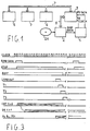
- Figure 1 shows in block diagram a typical data processing system comprising the digital apparatus of the present invention.
- Such apparatus is positioned between a drive device 2 for a mass storage 2A and a controller 3.
- the system of fig. 1 further comprises a central processor 4, a peripheral controller 5 and a main memory 6.
- Central processor 4, main memory 6 and controllers 3, 5 are connected each other by means of a plurality of leads or system bus 7 through which data, addresses and control signals can be exchanged.
- a standard circuit chip such as the 1791 integrated circuit chip, manufactured by Western Digital Corporation, can be used as controller 3.
- Controller 3 and drive device 2 exchange a plurality of control and information signals through a channel or bus 8.
- the recovery apparatus 1 must supply controller 3 with a square wave signal RDCLK and with a pulse train RD DATA at logical level 0, each pulse corresponding to a magnetic flux transition detected on recording media.
- Pulses RD DATA and window signal RD CLK have only to fulfill the condition that each pulse RD DATA occur entirely within a half wave (or window) of signal RD CLK.
- the pulse position relative to window signal RD CLK and the pulse length can be arbitrary. However, it is preferred that the length of a pulse RD DATA fall in the range of 100 to 250 nsec. and the delay of the beginning or end of a pulse relative to the transition of window signal RD CLK should be no longer than 40 nsec.
- Controller 3 does not need to be informed of whether each of the pulses RD DATA corresponds to a timing transition or to a data transition.
- the controller is able to distinguish between such transition from the pattern read out in response to the well known synchronization and "address mark" fields.
- the period of the timing or window signal can be variable and each of the two signals half waves may have a different length.
- Device 2 supplies digital apparatus 1 with a pulse RAW DATA in response to each detected magnetic flux transition. Since the disclosed system is intended to recover FM and MFM recorded information, the time intervals between subsequent pulses RAW DATA are indicative of such information.
- Apparatus 1 in response to the pulse train RAW DATA received as an input, supplies controller 3 with the window signal RD CLK and with the pulses RD DATA which correspond to the pulses RAW DATA suitably positioned relative to window signal RD CLK. Controller 3 is able by means of signal RD CLK to detect the information bits within the pulse train RD DATA and make them available in parallel form to system bus 7.
- FIG. 2 shows in block diagram form, the digital apparatus 1 of Fig. 1 which corresponds to the present invention.
- Apparatus 1 essentially comprises an oscillator 10, a timing unit 20, a logical unit 30 for measuring the interval duration between subsequent input pulses, a logical unit 40 for correcting such duration according to a speed difference as to a preestablished speed, a logic unit 50 for the peack shift recovery and the discrimination of the nominal duration corresponding to each interval, a logic unit 60 for reconstructing the read pulse train RD DATA within a window signal RD CLK generated by unit 60 itself and a unit 70 measuring and determining the speed difference as to a preestablished speed.
- Oscillator 10 supplies units 20, 30 and 40 with a square wave signal CLOCK having a frequency of 8 MHz.
- Timing unit 20 is activated by each of the pulses RAW DATA and supplies a plurality of timing signals REST, STOP, T1, T2, T3, LOAD OUT, to units 30, 50, 60, 70 in order to control and synchronize their operation.
- signal LOAD OUT is sent to units 50, 60 while signals REST, STOP are sent to unit 30 and signals T1, T2, T3 are sent to unit 70.
- Timing unit 20 can be embodied in several ways, with shift registers, delay lines and particularly with the same components and connections shown in Fig. 3 -of the already mentioned European patent application, therefore any further description is unnecessary.
- Fig. 3 shows in timing diagram the signals generated by the oscillator and by unit 20 together with other signals which will be considered later on.
- Diagram CLOCK is representative of signal CLOCK generated by oscillator 10.
- Diagram RAW DATA is representative of the read pulses received from unit 20.
- the read pulses appear as aynchronous events as to signal CLOCK and at variable time intervals owing to the magnetic media speed errors and to the peak shift.
- signal STOP rises to 1 and is kept at 1 for a duration of 19 CLOCK periods.
- Signal LOAD OUT, T1, T2, T3 rise to logical level 1 for the duration of two CLOCK periods, respectively after 16, 17, 18, 19 CLOCK periods from signal STOP rising.
- the sequence is triggered by pulse RAW DATA and, when the sequence is exhausted unit 20 remains unactive until a new trigger pulse is received.
- Measuring unit 30 is constituted by a six cell binary counter (practically two integrated counters as shown in Fig. 4 of the already mentioned patent application) which is reset by signal REST at logical level 0 and increments at each CLOCK pulse received on a clock input for the whole time signal STOP, applied to a control input, is at logical level O.
- Counter 3 stops when signal STOP is at logical level 1.
- the measurement is affected by an uncertainty owing to the asynchronous raising of pulses RAW DATA as to the CLOCK pulses.
- the maximum value of such uncertainty is equal to two CLOCK periods that is 250 ns (t125nsec.).
- Binary code CNT1 ⁇ 6 remains unchanged for the whole time signal STOP is at logical level 1 and is applied in input to speed difference recovery unit 40 through channel CNT.
- Unit 40 consists of a permanent memory, having for instance a capacity of 2K bytes.
- a binary code AO-4 is present on channel ⁇ V representative of the speed difference as to the media nominal value.
- Memory 40 acts as transcoder and changes a code ONT1+6 received on channel CNT to a 5-bit code SR 1+5 representative of an interval duration between read pulses corrected in accordance to code ⁇ 0+4 that is without speed error.
- Code SR 1 ⁇ 5 is applied, through channel SR, to peak shift recovery unit 50.
- unit 50 is constituted by a permanent memory 51, having for instance a capacity of 2K bytes and by an 8-bit latch register 52.
- Memory 51 is provided with 11 address inputs 11+11.
- the remaining 6 inputs I6 ⁇ 11 are connected to six of the eight outputs of register 52.
- the outputs of memory 51 are connected to the inputs of register 52.
- the information in output from memory 51 is loaded into register 52 when the register is enabled by the rising edge of periodical signal LOAD OUT.
- peak shift recovery unit 50 operates as follows.
- Memory 51 is addressed by a code SR 1+5 representative of the measured actual duration DE N , corrected as concerns a possible speed error of an interval N between two read pulses n-1 and n.
- Memory 51 contains transcoding codes which perform such discrimination and, for each addressable position, that is for each pair of information DE N , PS n - 1 , supply in output the pair of information DN N , PS N , that is a 2 bit binary code Ao, Bo, specifying whether the nominal duration is 4, 6, 8, wsec., and a six bit binary code PS 1-6, specifying with a bit PS 1, if the peak shift is positive or negative and with the remaining bits the peak shift entity.
- the codes A0, BO and PS 1+6 are loaded into register 52 and from there respectively sent to two inputs of unit 60 (code AO, BO) and to address inputs l6+11 of memory 51.
- lead 53 connects that register 52 output on which information PS1 is present to an input of unit 70.
- peak shift recovery unit 50 is quite identical (apart from connection 53) to and operates in the same way as the corresponding peak shift recovery unit described in the mentioned European patent application so that any detailed description is not required.
- the transcoding codes recorded into memory 51 may represent the actually detected entity of peak shift PS and not an information related to it (that is the actual duration of an interval DE N and the nominal duration DN N and DN N - 1 of the same interval or of the preceding one) as disclosed by the mentioned application.
- unit 70 allows to recover such kind of error.
- Logic unit 60 timed by signals CLOCK and LOAD OUT, supplies in output according to code AO, A0, a timing window signal RD CLK and a data signal RD DATA, which can be detected by controller (Fig. 1). Since logic unit 60 is identical to the one disclosed by the mentioned application and its description is unessential for the invention understanding, reference is made to the mentioned application for its architecture and operation details.
- Unit 70 comprises a first counter 71, a second bidirectional counter 72, a register 73, a permanent memory 74, a NOT logical element 75 and a two input logic AND gate 76.
- Counter 71 for instance of the type available on the market with code 74LS169 is set for the cyclical reckoning of 8 pulses.
- Input UP/DOWN is connected to a logic level 0 source in order to increment.
- Counter 71 has a carry output CY normally at logical level 1 which falls to logical level O when the counter reaches its maximum counting status.
- the CY output is connected to input LD of counter 71 and its clock input receives timing pulses T3 from unit 20.
- counter 71 increments at each rising edge of signal T3 applied to input CK.
- Counter 71 evolution is therefore cyclical with a period corresponding to the reception of 8 pulses T3 equal to 8 read intervals between read pulses.
- Counter 72 of the same type of counter 71, has its present input of binary weight 8 connected to a logic "1" while its preset inputs of binary weights 0, 2, 4 and its enabling input EN are connected to a logic "O".
- Timing pulses T2, generated by unit 20, are applied to CLOCK input CK.
- Input LD is connected to carry output CY of counter 71.
- Input UP/DOWN of counter 72 is connected to lead 53 and therefore periodically receives a signal indicating, with its logic level, if the last detected peak shift is positive or negative.
- the status reached by counter 72 at reception of the seventh pulses T2 therefore changes according to the number of negative or positive peak shift.
- the 3 most significant outputs of counter 72 are connected to as many inputs of a latch register 73.
- the register is periodically loaded, at the end of a counting cycle of counters 71, 72 and before the counters are preset.
- loading input LD of counter 73 is connected to the output of AND gate 76 which receives at a first input timing signal T1 and at a second input signal CY through NOT 75.
- register 73 The outputs of register 73 are connected to as many address inputs of permanent memory 74 which, acting as transcoder, generates binary code ⁇ V1 ⁇ 5 in output on channel AV.
- This code is sent in feedback to the inputs of register 73 as well as to corresponding address inputs of memory or speed error correction unit 40, as already explained.
- Unit 70 operates in conceptually simple way.
- unit 70 generates in output a speed error code AV defining an actual speed of the magnetic media
- This information is used to correct the measured duration of the intervals between read pulses, therefore the corrected duration is affected by peak shift error only.
- the peak shifts of the several pulses cannot accumulate that is, on average, during a certain number of subsequent read intervals, the peak shifts detected for the several read pulses must be positive and negative in equal number, that is their numerical difference must be zero or very near to zero.
- the pair of information APS and AV is used to address memory 74 to a location generating in output a new speed error code ⁇ V' compensating such unadequacy.
- the compensation process also recover possible error accumulation due to the discrete nature of the duration measurement.
- the compensation process takes place in a continuous periodic way with the updating of speed error AV at each period consisting of 8 intervals between subsequent read pulses, that is in the worst case of intervals with a nominal duration of 8 ⁇ sec. and a speed difference in defect of 10% each 70 ⁇ sec., corresponding to a minimum frequency of 14KHertz.
- This frequency is much higher than the speed variation frequency of the magnetic media.
- the relationship between the pair of information ⁇ PS, AV and the new updated code ⁇ V' can be widely chosen.
- the gain of the loop be lower than 1, that is the correcting action be not higher than the cause giving rise to it, and that new value ⁇ V' differ from the previous one only for values of APS equal to ⁇ 5, ⁇ 7.
- the relation may even be non linear.
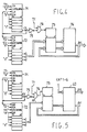
- FIG. 2 and 4 shows a preferred embodiment of the apparatus object of the present invention. Several changes can be made without departing from the scope of the invention.
- Fig. 5 shows a possible variant which can be used to minimize the number of permanent memories which are used.
- memory 74 of fig. 4 is substituted by memory 40 in its operation.
- Register 73 latches AP generated by counter 72, together with code AV, in this case a three bit code representative of the previously measured speed error.
- the outputs of register 73 are connected to corresponding address inputs of memory 40 receiving code CNT 1+6 on the other address inputs.
- Memory 40 according to the address codes, generates in output a code SR 1+5 with duration corrected as to the speed error and a new three bit code ⁇ V' representative of a new speed error updated according to code APS.
- code APS which can be constituted by only two bits instead of 3 bits, by cutting the peak shifts counting to a lesser number of intervals, for instance 3 or 5.
- ⁇ PS can clearly assume values +5, +3, +1, -1, -3, -5.
Landscapes
- Engineering & Computer Science (AREA)
- Signal Processing (AREA)
- Signal Processing For Digital Recording And Reproducing (AREA)
Claims (3)
Applications Claiming Priority (2)
| Application Number | Priority Date | Filing Date | Title |
|---|---|---|---|
| IT20007/85A IT1200426B (it) | 1985-03-21 | 1985-03-21 | Apparato digitale per sistema di recupero di informazioni binarie registrate su supporti magnetici |
| IT2000785 | 1985-03-21 |
Publications (3)
| Publication Number | Publication Date |
|---|---|
| EP0195368A2 EP0195368A2 (de) | 1986-09-24 |
| EP0195368A3 EP0195368A3 (en) | 1987-12-23 |
| EP0195368B1 true EP0195368B1 (de) | 1990-03-07 |
Family
ID=11163062
Family Applications (1)
| Application Number | Title | Priority Date | Filing Date |
|---|---|---|---|
| EP86103372A Expired - Lifetime EP0195368B1 (de) | 1985-03-21 | 1986-03-13 | Digitales Gerät für ein Datenwiedergewinnungssystem |
Country Status (5)
| Country | Link |
|---|---|
| US (1) | US4714968A (de) |
| EP (1) | EP0195368B1 (de) |
| JP (1) | JPS61239465A (de) |
| DE (1) | DE3669411D1 (de) |
| IT (1) | IT1200426B (de) |
Families Citing this family (9)
| Publication number | Priority date | Publication date | Assignee | Title |
|---|---|---|---|---|
| IT1185412B (it) * | 1985-10-10 | 1987-11-12 | Honeywell Inf Systems | Tseparatore digitale di dati |
| IT1185411B (it) * | 1985-10-10 | 1987-11-12 | Honeywell Inf Systems | Separatore digitale di dati |
| GB2205467B (en) * | 1987-05-28 | 1992-02-12 | Apple Computer | Disk drive controller |
| JPH069106B2 (ja) * | 1987-07-22 | 1994-02-02 | シャープ株式会社 | ディジタルデ−タ検出器 |
| US4851932A (en) * | 1988-01-29 | 1989-07-25 | Storage Technology Corporation | Adaptive compensation circuit for moving data storage media |
| US5212445A (en) * | 1991-02-13 | 1993-05-18 | Seagate Technology, Inc. | Method and apparatus for detection and identification of flaws in a magnetic medium by measuring the width of pulses stored on the medium |
| US5335118A (en) * | 1992-07-22 | 1994-08-02 | Seagate Technology, Inc. | Disc drive with write precompensation using window/pulse timing measurements |
| JP3345515B2 (ja) * | 1994-08-31 | 2002-11-18 | アイワ株式会社 | ピークシフト補正回路およびそれを使用した磁気記録媒体再生装置 |
| JP3521239B2 (ja) * | 1994-12-20 | 2004-04-19 | シャープ株式会社 | ディスクドライブ装置 |
Citations (1)
| Publication number | Priority date | Publication date | Assignee | Title |
|---|---|---|---|---|
| GB2080658A (en) * | 1980-07-11 | 1982-02-03 | Tokyo Shibaura Electric Co | Input data synchronizing circuit |
Family Cites Families (8)
| Publication number | Priority date | Publication date | Assignee | Title |
|---|---|---|---|---|
| IT1007175B (it) * | 1973-02-08 | 1976-10-30 | Siemens Ag | Circuito correttore digitale per correggere le sequenze di impulsi di lettura fornite da una memoria a strato magnetico |
| US3864735A (en) * | 1973-09-12 | 1975-02-04 | Burroughs Corp | Read/write system for high density magnetic recording |
| US4222080A (en) * | 1978-12-21 | 1980-09-09 | International Business Machines Corporation | Velocity tolerant decoding technique |
| US4344039A (en) * | 1979-03-13 | 1982-08-10 | Sanyo Electric Co., Ltd. | Demodulating circuit for self-clocking-information |
| US4298956A (en) * | 1979-05-14 | 1981-11-03 | Honeywell Information Systems Inc. | Digital read recovery with variable frequency compensation using read only memories |
| US4245264A (en) * | 1979-07-19 | 1981-01-13 | Control Systems, Inc. | Apparatus and method for digitally synchronizing the timing of a sequence of electrical output pulses in accordance with a selectable, permissably non-linear function of the timing of a sequence of electrical input pulses |
| US4281356A (en) * | 1979-11-28 | 1981-07-28 | R. C. Sanders Technology Systems, Inc. | Magnetic disk memory |
| US4393458A (en) * | 1980-02-06 | 1983-07-12 | Sperry Corporation | Data recovery method and apparatus using variable window |
-
1985
- 1985-03-21 IT IT20007/85A patent/IT1200426B/it active
-
1986
- 1986-03-03 US US06/835,415 patent/US4714968A/en not_active Expired - Fee Related
- 1986-03-13 DE DE8686103372T patent/DE3669411D1/de not_active Expired - Lifetime
- 1986-03-13 EP EP86103372A patent/EP0195368B1/de not_active Expired - Lifetime
- 1986-03-20 JP JP61063871A patent/JPS61239465A/ja active Pending
Patent Citations (1)
| Publication number | Priority date | Publication date | Assignee | Title |
|---|---|---|---|---|
| GB2080658A (en) * | 1980-07-11 | 1982-02-03 | Tokyo Shibaura Electric Co | Input data synchronizing circuit |
Also Published As
| Publication number | Publication date |
|---|---|
| IT1200426B (it) | 1989-01-18 |
| EP0195368A2 (de) | 1986-09-24 |
| IT8520007A0 (it) | 1985-03-21 |
| JPS61239465A (ja) | 1986-10-24 |
| EP0195368A3 (en) | 1987-12-23 |
| DE3669411D1 (de) | 1990-04-12 |
| US4714968A (en) | 1987-12-22 |
Similar Documents
| Publication | Publication Date | Title |
|---|---|---|
| US4596981A (en) | Synchronizing signal detecting circuit in a digital signal transmitting system | |
| USRE33665E (en) | Digital signal detecting and compensating circuit with adjustable window signal | |
| US4423498A (en) | Control apparatus for a recording medium drive motor in a digital information reproducing apparatus | |
| US4425646A (en) | Input data synchronizing circuit | |
| US4644420A (en) | Circuit and methodology for reading and tracking binary data from magnetic tape independently of the data pattern on the tape | |
| US4215430A (en) | Fast synchronization circuit for phase locked looped decoder | |
| US4449061A (en) | Wave-shaping circuit for digital signal | |
| EP0195368B1 (de) | Digitales Gerät für ein Datenwiedergewinnungssystem | |
| US4472686A (en) | Circuit for reproducing and demodulating modulated digital signals | |
| US4672482A (en) | Digital apparatus for magnetic media data recovery system | |
| US4344039A (en) | Demodulating circuit for self-clocking-information | |
| EP0267035A2 (de) | Datenglätter für eine Backup-Kassette eines Bandgerätes | |
| US4901301A (en) | Region detection system for detecting empty sectors on a recording medium | |
| US5386405A (en) | Disk apparatus having a read error retry function | |
| US5892631A (en) | Method and an arrangement for detecting state transitions in a read signal during a bit cell timing window | |
| US4742403A (en) | Digital data separator | |
| US3631422A (en) | System for detection of data time interval measurement | |
| US5396109A (en) | Bit clock regenerating circuit and data regenerating method | |
| US5175655A (en) | Method and apparatus for verifying a signal recorded in an encoded form on a medium | |
| JP3662985B2 (ja) | 同期及びビット情報検出装置 | |
| US4008488A (en) | Magnetic recording data decoding system | |
| EP0222133B1 (de) | Trennschaltung für digitale Daten | |
| US3646546A (en) | Split-phase adaptive decoding electronics | |
| US6895174B2 (en) | Frame number detecting device | |
| EP0428411B1 (de) | Informationsverarbeitungsgerät |
Legal Events
| Date | Code | Title | Description |
|---|---|---|---|
| PUAI | Public reference made under article 153(3) epc to a published international application that has entered the european phase |
Free format text: ORIGINAL CODE: 0009012 |
|
| AK | Designated contracting states |
Kind code of ref document: A2 Designated state(s): DE FR GB NL |
|
| PUAL | Search report despatched |
Free format text: ORIGINAL CODE: 0009013 |
|
| RAP1 | Party data changed (applicant data changed or rights of an application transferred) |
Owner name: HONEYWELL BULL ITALIA S.P.A. |
|
| AK | Designated contracting states |
Kind code of ref document: A3 Designated state(s): DE FR GB NL |
|
| 17P | Request for examination filed |
Effective date: 19880212 |
|
| RAP1 | Party data changed (applicant data changed or rights of an application transferred) |
Owner name: BULL HN INFORMATION SYSTEMS ITALIA S.P.A. |
|
| 17Q | First examination report despatched |
Effective date: 19890615 |
|
| GRAA | (expected) grant |
Free format text: ORIGINAL CODE: 0009210 |
|
| AK | Designated contracting states |
Kind code of ref document: B1 Designated state(s): DE FR GB NL |
|
| REF | Corresponds to: |
Ref document number: 3669411 Country of ref document: DE Date of ref document: 19900412 |
|
| ET | Fr: translation filed | ||
| PLBE | No opposition filed within time limit |
Free format text: ORIGINAL CODE: 0009261 |
|
| STAA | Information on the status of an ep patent application or granted ep patent |
Free format text: STATUS: NO OPPOSITION FILED WITHIN TIME LIMIT |
|
| 26N | No opposition filed | ||
| PGFP | Annual fee paid to national office [announced via postgrant information from national office to epo] |
Ref country code: FR Payment date: 19920326 Year of fee payment: 7 |
|
| PGFP | Annual fee paid to national office [announced via postgrant information from national office to epo] |
Ref country code: NL Payment date: 19920331 Year of fee payment: 7 |
|
| PGFP | Annual fee paid to national office [announced via postgrant information from national office to epo] |
Ref country code: DE Payment date: 19930219 Year of fee payment: 8 |
|
| PGFP | Annual fee paid to national office [announced via postgrant information from national office to epo] |
Ref country code: GB Payment date: 19930302 Year of fee payment: 8 |
|
| PG25 | Lapsed in a contracting state [announced via postgrant information from national office to epo] |
Ref country code: NL Effective date: 19931001 |
|
| NLV4 | Nl: lapsed or anulled due to non-payment of the annual fee | ||
| PG25 | Lapsed in a contracting state [announced via postgrant information from national office to epo] |
Ref country code: FR Effective date: 19931130 |
|
| REG | Reference to a national code |
Ref country code: FR Ref legal event code: ST |
|
| PG25 | Lapsed in a contracting state [announced via postgrant information from national office to epo] |
Ref country code: GB Effective date: 19940313 |
|
| GBPC | Gb: european patent ceased through non-payment of renewal fee |
Effective date: 19940313 |
|
| PG25 | Lapsed in a contracting state [announced via postgrant information from national office to epo] |
Ref country code: DE Effective date: 19941201 |