EP0192553B1 - Stromversorgungsgerät mit hoher Gleichspannung, insbesondere für eine röntgenstrahlenemittierende Röhre - Google Patents
Stromversorgungsgerät mit hoher Gleichspannung, insbesondere für eine röntgenstrahlenemittierende Röhre Download PDFInfo
- Publication number
- EP0192553B1 EP0192553B1 EP86400265A EP86400265A EP0192553B1 EP 0192553 B1 EP0192553 B1 EP 0192553B1 EP 86400265 A EP86400265 A EP 86400265A EP 86400265 A EP86400265 A EP 86400265A EP 0192553 B1 EP0192553 B1 EP 0192553B1
- Authority
- EP
- European Patent Office
- Prior art keywords
- power supply
- high voltage
- line
- inverter
- voltage
- Prior art date
- Legal status (The legal status is an assumption and is not a legal conclusion. Google has not performed a legal analysis and makes no representation as to the accuracy of the status listed.)
- Expired - Lifetime
Links
- 230000001105 regulatory effect Effects 0.000 claims description 5
- 238000010200 validation analysis Methods 0.000 claims description 4
- 238000001914 filtration Methods 0.000 claims description 2
- 238000010586 diagram Methods 0.000 description 6
- 230000010355 oscillation Effects 0.000 description 4
- 239000003990 capacitor Substances 0.000 description 3
- 230000002349 favourable effect Effects 0.000 description 3
- 230000000295 complement effect Effects 0.000 description 2
- 230000000630 rising effect Effects 0.000 description 2
- 238000001228 spectrum Methods 0.000 description 2
- 230000000712 assembly Effects 0.000 description 1
- 238000000429 assembly Methods 0.000 description 1
- 230000000052 comparative effect Effects 0.000 description 1
- 230000001419 dependent effect Effects 0.000 description 1
- 230000000694 effects Effects 0.000 description 1
- 238000009499 grossing Methods 0.000 description 1
- 230000002401 inhibitory effect Effects 0.000 description 1
- 238000009434 installation Methods 0.000 description 1
- 238000009413 insulation Methods 0.000 description 1
- 238000005259 measurement Methods 0.000 description 1
- 230000036962 time dependent Effects 0.000 description 1
- 238000004804 winding Methods 0.000 description 1
Images
Classifications
-
- H—ELECTRICITY
- H05—ELECTRIC TECHNIQUES NOT OTHERWISE PROVIDED FOR
- H05G—X-RAY TECHNIQUE
- H05G1/00—X-ray apparatus involving X-ray tubes; Circuits therefor
- H05G1/08—Electrical details
- H05G1/26—Measuring, controlling or protecting
- H05G1/30—Controlling
- H05G1/32—Supply voltage of the X-ray apparatus or tube
-
- H—ELECTRICITY
- H02—GENERATION; CONVERSION OR DISTRIBUTION OF ELECTRIC POWER
- H02M—APPARATUS FOR CONVERSION BETWEEN AC AND AC, BETWEEN AC AND DC, OR BETWEEN DC AND DC, AND FOR USE WITH MAINS OR SIMILAR POWER SUPPLY SYSTEMS; CONVERSION OF DC OR AC INPUT POWER INTO SURGE OUTPUT POWER; CONTROL OR REGULATION THEREOF
- H02M3/00—Conversion of DC power input into DC power output
- H02M3/22—Conversion of DC power input into DC power output with intermediate conversion into AC
- H02M3/24—Conversion of DC power input into DC power output with intermediate conversion into AC by static converters
- H02M3/28—Conversion of DC power input into DC power output with intermediate conversion into AC by static converters using discharge tubes with control electrode or semiconductor devices with control electrode to produce the intermediate AC
- H02M3/325—Conversion of DC power input into DC power output with intermediate conversion into AC by static converters using discharge tubes with control electrode or semiconductor devices with control electrode to produce the intermediate AC using devices of a triode or a transistor type requiring continuous application of a control signal
- H02M3/335—Conversion of DC power input into DC power output with intermediate conversion into AC by static converters using discharge tubes with control electrode or semiconductor devices with control electrode to produce the intermediate AC using devices of a triode or a transistor type requiring continuous application of a control signal using semiconductor devices only
- H02M3/337—Conversion of DC power input into DC power output with intermediate conversion into AC by static converters using discharge tubes with control electrode or semiconductor devices with control electrode to produce the intermediate AC using devices of a triode or a transistor type requiring continuous application of a control signal using semiconductor devices only in push-pull configuration
- H02M3/3376—Conversion of DC power input into DC power output with intermediate conversion into AC by static converters using discharge tubes with control electrode or semiconductor devices with control electrode to produce the intermediate AC using devices of a triode or a transistor type requiring continuous application of a control signal using semiconductor devices only in push-pull configuration with automatic control of output voltage or current
-
- H—ELECTRICITY
- H02—GENERATION; CONVERSION OR DISTRIBUTION OF ELECTRIC POWER
- H02M—APPARATUS FOR CONVERSION BETWEEN AC AND AC, BETWEEN AC AND DC, OR BETWEEN DC AND DC, AND FOR USE WITH MAINS OR SIMILAR POWER SUPPLY SYSTEMS; CONVERSION OF DC OR AC INPUT POWER INTO SURGE OUTPUT POWER; CONTROL OR REGULATION THEREOF
- H02M5/00—Conversion of AC power input into AC power output, e.g. for change of voltage, for change of frequency, for change of number of phases
- H02M5/40—Conversion of AC power input into AC power output, e.g. for change of voltage, for change of frequency, for change of number of phases with intermediate conversion into DC
- H02M5/42—Conversion of AC power input into AC power output, e.g. for change of voltage, for change of frequency, for change of number of phases with intermediate conversion into DC by static converters
- H02M5/44—Conversion of AC power input into AC power output, e.g. for change of voltage, for change of frequency, for change of number of phases with intermediate conversion into DC by static converters using discharge tubes or semiconductor devices to convert the intermediate DC into AC
- H02M5/453—Conversion of AC power input into AC power output, e.g. for change of voltage, for change of frequency, for change of number of phases with intermediate conversion into DC by static converters using discharge tubes or semiconductor devices to convert the intermediate DC into AC using devices of a triode or transistor type requiring continuous application of a control signal
- H02M5/458—Conversion of AC power input into AC power output, e.g. for change of voltage, for change of frequency, for change of number of phases with intermediate conversion into DC by static converters using discharge tubes or semiconductor devices to convert the intermediate DC into AC using devices of a triode or transistor type requiring continuous application of a control signal using semiconductor devices only
-
- H—ELECTRICITY
- H02—GENERATION; CONVERSION OR DISTRIBUTION OF ELECTRIC POWER
- H02M—APPARATUS FOR CONVERSION BETWEEN AC AND AC, BETWEEN AC AND DC, OR BETWEEN DC AND DC, AND FOR USE WITH MAINS OR SIMILAR POWER SUPPLY SYSTEMS; CONVERSION OF DC OR AC INPUT POWER INTO SURGE OUTPUT POWER; CONTROL OR REGULATION THEREOF
- H02M7/00—Conversion of AC power input into DC power output; Conversion of DC power input into AC power output
- H02M7/42—Conversion of DC power input into AC power output without possibility of reversal
- H02M7/44—Conversion of DC power input into AC power output without possibility of reversal by static converters
- H02M7/48—Conversion of DC power input into AC power output without possibility of reversal by static converters using discharge tubes with control electrode or semiconductor devices with control electrode
- H02M7/53—Conversion of DC power input into AC power output without possibility of reversal by static converters using discharge tubes with control electrode or semiconductor devices with control electrode using devices of a triode or transistor type requiring continuous application of a control signal
- H02M7/537—Conversion of DC power input into AC power output without possibility of reversal by static converters using discharge tubes with control electrode or semiconductor devices with control electrode using devices of a triode or transistor type requiring continuous application of a control signal using semiconductor devices only, e.g. single switched pulse inverters
- H02M7/5387—Conversion of DC power input into AC power output without possibility of reversal by static converters using discharge tubes with control electrode or semiconductor devices with control electrode using devices of a triode or transistor type requiring continuous application of a control signal using semiconductor devices only, e.g. single switched pulse inverters in a bridge configuration
- H02M7/53871—Conversion of DC power input into AC power output without possibility of reversal by static converters using discharge tubes with control electrode or semiconductor devices with control electrode using devices of a triode or transistor type requiring continuous application of a control signal using semiconductor devices only, e.g. single switched pulse inverters in a bridge configuration with automatic control of output voltage or current
- H02M7/53873—Conversion of DC power input into AC power output without possibility of reversal by static converters using discharge tubes with control electrode or semiconductor devices with control electrode using devices of a triode or transistor type requiring continuous application of a control signal using semiconductor devices only, e.g. single switched pulse inverters in a bridge configuration with automatic control of output voltage or current with digital control
-
- H—ELECTRICITY
- H05—ELECTRIC TECHNIQUES NOT OTHERWISE PROVIDED FOR
- H05G—X-RAY TECHNIQUE
- H05G1/00—X-ray apparatus involving X-ray tubes; Circuits therefor
- H05G1/08—Electrical details
- H05G1/10—Power supply arrangements for feeding the X-ray tube
- H05G1/20—Power supply arrangements for feeding the X-ray tube with high-frequency AC; with pulse trains
Definitions
- the present invention relates to a continuous high voltage power supply, in particular for an X-ray emitter tube. It can nevertheless be applied to other fields.
- the affected power supplies are intended to be connected to a general electrical distribution network.
- the object of the present invention is to remedy the drawbacks mentioned by proposing a power supply where the high voltage is chopped. It is produced only for short periods corresponding to the peaks of the alternations of the single-phase network. In this way, no energy is drawn from the network when it is at low voltage: the tube current during these stops is zero. There is then no excessive Joule loss in the network.
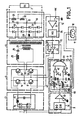
- Figure 1 shows a high voltage power supply according to the invention. It receives electrical energy from a single-phase network 1 and transforms it into high direct voltage intended to supply an X-ray tube 2. It comprises first means 3 of full-wave rectification and filtering of the single-phase voltage. An inverter 4 supplied by the rectifier 3 delivers in voltage boosting means 5. In one example, the inverter oscillates at several tens of kilohertz. Second rectifier means 6 rectify and filter the high alternating voltage supplied by the transformer 5. They deliver a high direct voltage in the tube 2. An important characteristic of the invention is that this chain 3 - 6 operates to periodically withdraw from the energy from the network 1 under the control of synchronization means 7. These synchronization means include means 8 for recognizing the phase of the network. They also include means 9 for varying the synchronization setting with respect to the phase of the network, or for varying the withdrawal times. The means 9 are in relation to commands 10 and 11 on which an operator can act.
- the power supply further comprises regulation means 12 which regulate the high voltage produced by the second rectifier 6 as a function of an ERV reference applied externally.
- the synchronization means 7 act on validation means 13 of the operation of the regulation means 12. In other words, when the synchronization means allow it, the regulated high voltage is discharged normally. When they no longer allow it, in particular during voltage dips in the single-phase signal from the network, the regulation chain is cut, the high voltage at the output is canceled.
- the first rectifying means 3 conventionally comprise double alternating rectifying means 14 in cascade with a low-pass filter 15.
- the inverter 4 conventionally comprises four power transistors mounted in pairs in cascade, 16 - 17 and 18 - 19, between the two outputs of the rectifier 3.
- the bases of the opposite diagonnaie transistors, 16-19 and 17-18, are connected together. They receive additional conduction orders via an inverter 20 of the validation means 13.
- the two cascades of transistors then function as PUSH - PULL type assemblies reversed from each other. Their midpoint, respectively 21 and 22 is connected to the voltage raising means 5.
- the means 5 comprise an oscillating circuit, with an inductance 23 and a capacity 24, tuned to a frequency slightly lower than the minimum frequency at which we waits to see the inverter vibrate 4.
- the natural frequency of this filter is 18 kilohertz.
- the inductance 23 represents the inductance 23 proper as well as the leakage inductance of a transformer 25 in series which is used for raising the voltage.
- the transformer 25 feeds into the second rectification means 6.
- These comprise two full-wave rectification circuits 26 and 27 respectively. They are each connected between a midpoint 28 of the transformer 25 and respectively one and the other of the ends of the secondary winding of this transformer.
- smoothing means comprising for example two capacitors 29 and 30 make it possible to filter the full-wave rectification of circuits 26 and 27 respectively.
- the high voltage then appears substantially flat. Capacities 29 and 30 are low because the rectified high alternating voltage is a high frequency voltage.
- the midpoint 35 of the rectifiers 26 - 27 is connected to ground. It allows the value of the high voltage produced to be divided by two, relative to it. The insulation constraints of the high voltage pads are then also halved.
- the interest of the oscillating circuit 23 - 24 lies in the sinusoidal aspect of the voltage which it produces.
- This sinusoidal voltage on the one hand crosses, more easily than a square signal of the same frequency, the transformer 25.
- the regular decrease of the current, as well as its regular growth, at each half-wave is favorable for a good destocking of the electronic charges stored at the time of saturation in the diodes of these rectifiers.
- This sinusoidal aspect is moreover favorable to the reduction of the reinjection of radio interference into the network 1.
- the regulation means 12 in fact comprise a frequency modulator 34 (VCO).
- VCO frequency modulator 34
- the oscillating circuit is slightly detuned by excess: the inverter vibrates for example at twenty kilohertzs while the oscillating circuit 23 -24 is tuned on 18 kilohertz.
- the oscillation frequency of the inverter is higher (for example 50 kilohertzs), the oscillating circuit is strongly detuned: it can pass less power.
- This frequency distribution is provided to minimize switching losses. Indeed at maximum high voltage, the oscillation frequency is the lowest, the switching losses are therefore the lowest. At minimum high voltage, the oscillation frequency is the highest, the switching losses are the highest; but it is not annoying since in this case the power required from the power supply is low.
- the regulation loop includes a comparator 31 which receives on a first input a signal coming from a divider bridge 32 - 33 (which measures the high voltage produced), and which receives on a second input a reference voltage VRE which represents the high voltage at which we want to operate the tube 2.
- the error signal produced by the comparator 31 is introduced into a frequency modulator 34. This produces for example a square signal at a frequency ultimately dependent on the reference voltage VRE.
- the square signal is applied at the same time as its complement on the corresponding bases of the transistors of the inverter 4.
- the synchronization means include means 8 for recognizing the phase of the sector signal.
- the means 8 comprise a full-wave rectifier 36 which flows into a comparator 37.
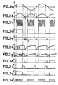
- the signal produced at the output of the means 8 is that which appears in FIG. 2e.
- the comparison voltage VC to which the full-wave rectified signal is compared is sufficiently low for the output signal from comparator 37 to have a rising edge 38 fairly close in time to the instant of zero crossing between two successive alternations.
- This phase identification signal is introduced into the means 9 to vary the timing.
- These include two RC circuits 38 - 39 and 40 - 41 respectively. The midpoints of these RC circuits are connected to first comparator inputs 42 and 43 respectively. Each comparator receives a threshold voltage at its second input: VS1 respectively and VS2.
- the circuits RC of the means 9 are each surmounted by a diode 47 or 48 to completely discharge the capacitors 39 or 41 at each change of half-wave.
- a diode 49 mounted in parallel at the output of comparator 37 promotes this discharge.
- Another special feature of RC circuits is that their time constant is adjustable.
- the resistors 38 and 40 can be adjusted by means of the graduated levers 10 and 11. By acting on these levers, the date of start-up as well as the date of shutdown of the inverter 4 is determined. duration.
- the validation circuit 13 comprises two logic gates AND respectively 45 and 46 receiving on a first of their inputs the signal from the AND gate 44. On their second input they receive the square signal, or its complementary, emanating from the modulator 34. These gates logic therefore deliver impulse signals comparable to that of the 2k diagram.
- the inverter operates. The X-ray tube is powered. Outside the durations at the bases of the inverter transistors are brought to zero, all these transistors are blocked, the X-ray tube is no longer supplied.
- Diagrams 2a to 2d respectively present the network signal, the rectified full-wave signal, the sinusoidal signal at the output of the inverter, and finally the filtered rectified high voltage signal applicable to the terminals of the X-ray tube.
- the oscillation frequency of the wavy signal is the same as the frequency of the signal delivered by logic gates 45 and 46.
- the duration a of operation of the inverter 4 is between dates where this phase is 40 ° and 140 °. .
- this way of acting has the effect of increasing the exposure time necessary for producing an X-ray photograph. In fact it is not.
- the peak value of the chopped DC voltage is of the order of 90% of the peak value of a half-wave rectified voltage, it can be established that the exposure times are almost identical.
- the images obtained in the invention are better since, during the entire installation, the supply voltage changes little. With a high voltage rectified double altemance (100 hertzs) the emitted spectrum borrows the whole range due to voltage dips.
Landscapes
- Engineering & Computer Science (AREA)
- Power Engineering (AREA)
- Health & Medical Sciences (AREA)
- General Health & Medical Sciences (AREA)
- Toxicology (AREA)
- X-Ray Techniques (AREA)
Claims (5)
Applications Claiming Priority (2)
| Application Number | Priority Date | Filing Date | Title |
|---|---|---|---|
| FR8501971 | 1985-02-12 | ||
| FR8501971A FR2577373B1 (fr) | 1985-02-12 | 1985-02-12 | Alimentation haute tension continue, notamment pour emetteur de rayons x |
Publications (2)
| Publication Number | Publication Date |
|---|---|
| EP0192553A1 EP0192553A1 (de) | 1986-08-27 |
| EP0192553B1 true EP0192553B1 (de) | 1990-04-25 |
Family
ID=9316177
Family Applications (1)
| Application Number | Title | Priority Date | Filing Date |
|---|---|---|---|
| EP86400265A Expired - Lifetime EP0192553B1 (de) | 1985-02-12 | 1986-02-07 | Stromversorgungsgerät mit hoher Gleichspannung, insbesondere für eine röntgenstrahlenemittierende Röhre |
Country Status (4)
| Country | Link |
|---|---|
| US (1) | US4680693A (de) |
| EP (1) | EP0192553B1 (de) |
| DE (1) | DE3670734D1 (de) |
| FR (1) | FR2577373B1 (de) |
Families Citing this family (13)
| Publication number | Priority date | Publication date | Assignee | Title |
|---|---|---|---|---|
| US4727469A (en) * | 1987-03-23 | 1988-02-23 | Reliance Comm/Tec Corporation | Control for a series resonant power converter |
| US4797803A (en) * | 1987-12-23 | 1989-01-10 | Dci Technology | Switching power supply VCO |
| US5189602A (en) * | 1989-05-12 | 1993-02-23 | General Electric Cgr S.A. | High-voltage generator with selective half-bridge and full-bridge operation |
| DE3928809A1 (de) * | 1989-08-31 | 1991-03-07 | Philips Patentverwaltung | Schaltungsanordnung zum speisen einer last |
| FR2666000B1 (fr) * | 1990-08-14 | 1996-09-13 | Gen Electric Cgr | Dispositif d'alimentation et de regulation en courant d'un filament de cathode d'un tube radiogene. |
| FR2665999B1 (fr) * | 1990-08-14 | 1994-01-28 | General Electric Cgr Sa | Dispositif d'obtention d'une tension continue reglable. |
| FR2672166B1 (fr) * | 1991-01-25 | 1995-04-28 | Gen Electric Cgr | Dispositif pour obtenir une tension continue a faible ondulation residuelle. |
| US5267138A (en) * | 1992-03-23 | 1993-11-30 | Creos International Ltd. | Driving and clamping power regulation technique for continuous, in-phase, full-duration, switch-mode resonant converter power supply |
| US6195272B1 (en) | 2000-03-16 | 2001-02-27 | Joseph E. Pascente | Pulsed high voltage power supply radiography system having a one to one correspondence between low voltage input pulses and high voltage output pulses |
| US6181580B1 (en) * | 2000-05-25 | 2001-01-30 | General Electric Company | Single-supply gridding and biasing circuitry |
| DE10228336C1 (de) * | 2002-06-25 | 2003-11-27 | Siemens Ag | Schaltungsanordnung und Verfahren zur Erzeugung einer Röntgenröhrenspannung, sowie Röntgengenerator und Röntgeneinrichtung |
| JP4392746B2 (ja) * | 2003-05-23 | 2010-01-06 | 株式会社日立メディコ | X線高電圧装置 |
| EA016999B1 (ru) * | 2009-06-24 | 2012-09-28 | Анатолий Яковлевич КАРТЕЛЕВ | Устройство для электрогидравлического воздействия на призабойную зону скважины |
Family Cites Families (10)
| Publication number | Priority date | Publication date | Assignee | Title |
|---|---|---|---|---|
| US3539812A (en) * | 1968-01-23 | 1970-11-10 | Westinghouse Electric Corp | Polyphase power supply for x-ray apparatus with means for preventing saturation in the transformer |
| DE2223371B2 (de) * | 1972-05-12 | 1976-09-02 | Siemens AG, 1000 Berlin und 8000 München | Roentgendiagnostikapparat mit einer regeleinrichtung fuer die roentgenroehrenspannung |
| JPS58959Y2 (ja) * | 1977-05-18 | 1983-01-08 | 株式会社東芝 | X線発生装置 |
| GB1602613A (en) * | 1977-06-24 | 1981-11-11 | Chloride Group Ltd | Converters |
| DE2802424A1 (de) * | 1978-01-20 | 1979-07-26 | Siemens Ag | Roentgendiagnostikgenerator mit einem seinen hochspannungstransformator speisenden wechselrichter |
| DE2917594A1 (de) * | 1979-04-30 | 1980-11-13 | Siemens Ag | Ein- oder zweipuls-roentgendiagnostikgenerator |
| US4301498A (en) * | 1979-10-31 | 1981-11-17 | Gould Advance Limited | Voltage converter apparatus having output regulating means |
| JPS5889075A (ja) * | 1981-11-24 | 1983-05-27 | Hitachi Ltd | 共振形スイツチング電源装置 |
| US4504895A (en) * | 1982-11-03 | 1985-03-12 | General Electric Company | Regulated dc-dc converter using a resonating transformer |
| IL73674A0 (en) * | 1983-12-22 | 1985-02-28 | Gen Electric | Inverter driver for x-ray generator |
-
1985
- 1985-02-12 FR FR8501971A patent/FR2577373B1/fr not_active Expired - Lifetime
-
1986
- 1986-02-07 EP EP86400265A patent/EP0192553B1/de not_active Expired - Lifetime
- 1986-02-07 DE DE8686400265T patent/DE3670734D1/de not_active Expired - Lifetime
- 1986-02-10 US US06/827,725 patent/US4680693A/en not_active Expired - Fee Related
Also Published As
| Publication number | Publication date |
|---|---|
| US4680693A (en) | 1987-07-14 |
| EP0192553A1 (de) | 1986-08-27 |
| FR2577373B1 (fr) | 1995-02-17 |
| FR2577373A1 (fr) | 1986-08-14 |
| DE3670734D1 (de) | 1990-05-31 |
Similar Documents
| Publication | Publication Date | Title |
|---|---|---|
| EP0192553B1 (de) | Stromversorgungsgerät mit hoher Gleichspannung, insbesondere für eine röntgenstrahlenemittierende Röhre | |
| FR2541531A1 (fr) | Procede pour creer un courant alternatif a partir d'un courant continu | |
| EP0720281B1 (de) | Elektronische Vorrichtung zur elektrischen Energieumwandlung | |
| FR2745446A1 (fr) | Circuit integre de correction de facteur de puissance | |
| EP0193435B1 (de) | Steuerschaltung für ein Schaltnetzteil mit automatischem Anlauf | |
| CA1237472A (fr) | Convertisseur de frequence statique de puissance | |
| FR2738417A1 (fr) | Convertisseur de tension continue a commutation douce | |
| EP1275196B1 (de) | Motor mit phasenwinkelvorlauf | |
| EP0329571B1 (de) | Schaltungsanordnung zur Überwachung der Entmagnetisierung für einen Sperrwandler mit primärseitiger und secundärseitiger Regelung | |
| FR2742277A1 (fr) | Dispositif d'alimentation a decoupage | |
| FR2508736A1 (fr) | Systeme d'alimentation | |
| EP3910775A1 (de) | Steuerung eines stromwandlers mit partitionierung | |
| FR2772154A1 (fr) | Circuit de commande pour la correction du facteur de puissance | |
| EP0193436A1 (de) | Steuerschaltung für ein Schaltnetzteil mit progressivem Anlauf | |
| FR2783370A1 (fr) | Dispositif d'alimentation a onduleur dont la puissance delivree est controlee | |
| FR2610461A1 (fr) | Convertisseur electronique courant alternatif-courant continu-courant alternatif | |
| FR2605168A1 (fr) | Circuit de commande en mode veille d'une alimentation a decoupage | |
| EP0176413B1 (de) | Gleichspannungsschaltnetzteil | |
| FR2539563A1 (fr) | Source de puissance alternative haute frequence | |
| EP1564876A1 (de) | Schweisseinrichtung mit sanfschaltendem Quasi-resonanzwechselrichter | |
| FR2768241A1 (fr) | Dispositif et procede de regulation a commande optimale d'un convertisseur a transistors | |
| EP1444768B1 (de) | Verfahren und einrichtung zur transformation einer gleichspannung und verwendung der einrichtung | |
| CA2170317C (fr) | Procede de commande pour courant electrique bidirectionnel et onduleur de tension a commutation douce | |
| FR2675000A1 (fr) | Procede et dispositif pour attenuer l'effet du radioparasitage par conduction sur le reseau alternatif polyphase. | |
| EP0928057B1 (de) | Hochspannungsschalter aus reihengeschalteten resonanten Zellen |
Legal Events
| Date | Code | Title | Description |
|---|---|---|---|
| PUAI | Public reference made under article 153(3) epc to a published international application that has entered the european phase |
Free format text: ORIGINAL CODE: 0009012 |
|
| AK | Designated contracting states |
Kind code of ref document: A1 Designated state(s): BE DE GB IT LU NL |
|
| 17P | Request for examination filed |
Effective date: 19860919 |
|
| 17Q | First examination report despatched |
Effective date: 19880108 |
|
| RAP1 | Party data changed (applicant data changed or rights of an application transferred) |
Owner name: GENERAL ELECTRIC CGR SA. |
|
| GRAA | (expected) grant |
Free format text: ORIGINAL CODE: 0009210 |
|
| AK | Designated contracting states |
Kind code of ref document: B1 Designated state(s): BE DE GB IT LU NL |
|
| ITF | It: translation for a ep patent filed | ||
| GBT | Gb: translation of ep patent filed (gb section 77(6)(a)/1977) | ||
| REF | Corresponds to: |
Ref document number: 3670734 Country of ref document: DE Date of ref document: 19900531 |
|
| PLBE | No opposition filed within time limit |
Free format text: ORIGINAL CODE: 0009261 |
|
| STAA | Information on the status of an ep patent application or granted ep patent |
Free format text: STATUS: NO OPPOSITION FILED WITHIN TIME LIMIT |
|
| PG25 | Lapsed in a contracting state [announced via postgrant information from national office to epo] |
Ref country code: LU Free format text: LAPSE BECAUSE OF NON-PAYMENT OF DUE FEES Effective date: 19910228 |
|
| 26N | No opposition filed | ||
| PGFP | Annual fee paid to national office [announced via postgrant information from national office to epo] |
Ref country code: GB Payment date: 19920124 Year of fee payment: 7 |
|
| PGFP | Annual fee paid to national office [announced via postgrant information from national office to epo] |
Ref country code: BE Payment date: 19920204 Year of fee payment: 7 |
|
| ITTA | It: last paid annual fee | ||
| PG25 | Lapsed in a contracting state [announced via postgrant information from national office to epo] |
Ref country code: GB Effective date: 19930207 |
|
| PG25 | Lapsed in a contracting state [announced via postgrant information from national office to epo] |
Ref country code: BE Effective date: 19930228 |
|
| PGFP | Annual fee paid to national office [announced via postgrant information from national office to epo] |
Ref country code: NL Payment date: 19930228 Year of fee payment: 8 |
|
| BERE | Be: lapsed |
Owner name: S.A. GENERAL ELECTRIC CGR Effective date: 19930228 |
|
| GBPC | Gb: european patent ceased through non-payment of renewal fee |
Effective date: 19930207 |
|
| PG25 | Lapsed in a contracting state [announced via postgrant information from national office to epo] |
Ref country code: NL Effective date: 19940901 |
|
| NLV4 | Nl: lapsed or anulled due to non-payment of the annual fee | ||
| PG25 | Lapsed in a contracting state [announced via postgrant information from national office to epo] |
Ref country code: IT Free format text: LAPSE BECAUSE OF NON-PAYMENT OF DUE FEES;WARNING: LAPSES OF ITALIAN PATENTS WITH EFFECTIVE DATE BEFORE 2007 MAY HAVE OCCURRED AT ANY TIME BEFORE 2007. THE CORRECT EFFECTIVE DATE MAY BE DIFFERENT FROM THE ONE RECORDED. Effective date: 20050207 |
|
| PGFP | Annual fee paid to national office [announced via postgrant information from national office to epo] |
Ref country code: DE Payment date: 20050331 Year of fee payment: 20 |