EP0191902A1 - Aufbausystem für Geräte der elektrischen Nachrichtentechnik - Google Patents
Aufbausystem für Geräte der elektrischen Nachrichtentechnik Download PDFInfo
- Publication number
- EP0191902A1 EP0191902A1 EP85112837A EP85112837A EP0191902A1 EP 0191902 A1 EP0191902 A1 EP 0191902A1 EP 85112837 A EP85112837 A EP 85112837A EP 85112837 A EP85112837 A EP 85112837A EP 0191902 A1 EP0191902 A1 EP 0191902A1
- Authority
- EP
- European Patent Office
- Prior art keywords
- plug
- magazines
- connectors
- backplane
- magazine
- Prior art date
- Legal status (The legal status is an assumption and is not a legal conclusion. Google has not performed a legal analysis and makes no representation as to the accuracy of the status listed.)
- Granted
Links
- 238000005516 engineering process Methods 0.000 title claims description 3
- 239000004020 conductor Substances 0.000 claims abstract description 22
- 230000013011 mating Effects 0.000 claims abstract description 3
- 238000010276 construction Methods 0.000 claims description 12
- 238000004891 communication Methods 0.000 claims description 6
- 238000006073 displacement reaction Methods 0.000 claims description 2
- 239000011159 matrix material Substances 0.000 description 11
- 238000010168 coupling process Methods 0.000 description 4
- 238000005859 coupling reaction Methods 0.000 description 4
- 238000004519 manufacturing process Methods 0.000 description 4
- 230000008878 coupling Effects 0.000 description 2
- 238000011161 development Methods 0.000 description 2
- 230000000712 assembly Effects 0.000 description 1
- 238000000429 assembly Methods 0.000 description 1
- 230000005540 biological transmission Effects 0.000 description 1
- 238000005476 soldering Methods 0.000 description 1
- 238000012546 transfer Methods 0.000 description 1
Images


Classifications
-
- H—ELECTRICITY
- H05—ELECTRIC TECHNIQUES NOT OTHERWISE PROVIDED FOR
- H05K—PRINTED CIRCUITS; CASINGS OR CONSTRUCTIONAL DETAILS OF ELECTRIC APPARATUS; MANUFACTURE OF ASSEMBLAGES OF ELECTRICAL COMPONENTS
- H05K1/00—Printed circuits
- H05K1/02—Details
- H05K1/0213—Electrical arrangements not otherwise provided for
- H05K1/0216—Reduction of cross-talk, noise or electromagnetic interference
- H05K1/0228—Compensation of cross-talk by a mutually correlated lay-out of printed circuit traces, e.g. for compensation of cross-talk in mounted connectors
-
- H—ELECTRICITY
- H05—ELECTRIC TECHNIQUES NOT OTHERWISE PROVIDED FOR
- H05K—PRINTED CIRCUITS; CASINGS OR CONSTRUCTIONAL DETAILS OF ELECTRIC APPARATUS; MANUFACTURE OF ASSEMBLAGES OF ELECTRICAL COMPONENTS
- H05K7/00—Constructional details common to different types of electric apparatus
- H05K7/14—Mounting supporting structure in casing or on frame or rack
- H05K7/1438—Back panels or connecting means therefor; Terminals; Coding means to avoid wrong insertion
- H05K7/1439—Back panel mother boards
-
- H—ELECTRICITY
- H05—ELECTRIC TECHNIQUES NOT OTHERWISE PROVIDED FOR
- H05K—PRINTED CIRCUITS; CASINGS OR CONSTRUCTIONAL DETAILS OF ELECTRIC APPARATUS; MANUFACTURE OF ASSEMBLAGES OF ELECTRICAL COMPONENTS
- H05K7/00—Constructional details common to different types of electric apparatus
- H05K7/14—Mounting supporting structure in casing or on frame or rack
- H05K7/1438—Back panels or connecting means therefor; Terminals; Coding means to avoid wrong insertion
- H05K7/1459—Circuit configuration, e.g. routing signals
-
- H—ELECTRICITY
- H05—ELECTRIC TECHNIQUES NOT OTHERWISE PROVIDED FOR
- H05K—PRINTED CIRCUITS; CASINGS OR CONSTRUCTIONAL DETAILS OF ELECTRIC APPARATUS; MANUFACTURE OF ASSEMBLAGES OF ELECTRICAL COMPONENTS
- H05K2201/00—Indexing scheme relating to printed circuits covered by H05K1/00
- H05K2201/04—Assemblies of printed circuits
- H05K2201/044—Details of backplane or midplane for mounting orthogonal PCBs
-
- H—ELECTRICITY
- H05—ELECTRIC TECHNIQUES NOT OTHERWISE PROVIDED FOR
- H05K—PRINTED CIRCUITS; CASINGS OR CONSTRUCTIONAL DETAILS OF ELECTRIC APPARATUS; MANUFACTURE OF ASSEMBLAGES OF ELECTRICAL COMPONENTS
- H05K2201/00—Indexing scheme relating to printed circuits covered by H05K1/00
- H05K2201/09—Shape and layout
- H05K2201/09209—Shape and layout details of conductors
- H05K2201/09218—Conductive traces
- H05K2201/09236—Parallel layout
-
- H—ELECTRICITY
- H05—ELECTRIC TECHNIQUES NOT OTHERWISE PROVIDED FOR
- H05K—PRINTED CIRCUITS; CASINGS OR CONSTRUCTIONAL DETAILS OF ELECTRIC APPARATUS; MANUFACTURE OF ASSEMBLAGES OF ELECTRICAL COMPONENTS
- H05K2201/00—Indexing scheme relating to printed circuits covered by H05K1/00
- H05K2201/09—Shape and layout
- H05K2201/09209—Shape and layout details of conductors
- H05K2201/09218—Conductive traces
- H05K2201/09245—Crossing layout
-
- H—ELECTRICITY
- H05—ELECTRIC TECHNIQUES NOT OTHERWISE PROVIDED FOR
- H05K—PRINTED CIRCUITS; CASINGS OR CONSTRUCTIONAL DETAILS OF ELECTRIC APPARATUS; MANUFACTURE OF ASSEMBLAGES OF ELECTRICAL COMPONENTS
- H05K2201/00—Indexing scheme relating to printed circuits covered by H05K1/00
- H05K2201/09—Shape and layout
- H05K2201/09209—Shape and layout details of conductors
- H05K2201/09218—Conductive traces
- H05K2201/09272—Layout details of angles or corners
-
- H—ELECTRICITY
- H05—ELECTRIC TECHNIQUES NOT OTHERWISE PROVIDED FOR
- H05K—PRINTED CIRCUITS; CASINGS OR CONSTRUCTIONAL DETAILS OF ELECTRIC APPARATUS; MANUFACTURE OF ASSEMBLAGES OF ELECTRICAL COMPONENTS
- H05K2201/00—Indexing scheme relating to printed circuits covered by H05K1/00
- H05K2201/09—Shape and layout
- H05K2201/09209—Shape and layout details of conductors
- H05K2201/09654—Shape and layout details of conductors covering at least two types of conductors provided for in H05K2201/09218 - H05K2201/095
- H05K2201/09709—Staggered pads, lands or terminals; Parallel conductors in different planes
Definitions
- the invention relates to a construction system for electrical communications equipment according to the preamble of claim 1.
- a construction system is known from German utility model 72 15 350. It consists of plug-in modules, which carry electrical components and connector strips on one edge. Several plug-in modules are inserted into a magazine from the front, which has a backplane on the back. This carries socket strips in which the connector strips engage. The socket strips are electrically connected to one another by means of conductor tracks on the backplane. Larger devices consist of several such magazines, which are electrically connected to each other by cable harnesses. These cable harnesses are made by hand, which is time-consuming and mistakes can creep in. Because of this manual work, the position of the individual wires in the cable harnesses also differs from specimen to specimen. The consequence of this is that their electrical properties, in particular the crosstalk attenuation between two wires or pairs of wires, are also different and unpredictable. This limits the usability of wire harnesses for message signals with higher frequencies.
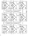
- FIG. 1 shows an overview plan of a three-stage switching network for a message switching system.
- Each stage consists of 16 sub-coupling fields.
- the construction system described above lends itself to the realization of such a switching matrix. So you will train the sub-switch modules as plug-in modules and arrange them in magazines sorted by level.
- Each sub-switching matrix consists of 256 coupling points KP arranged in a 16x16 matrix.
- the 16 sub-coupling fields i.e. the 16 plug-in modules G1 to G16 of a stage, are housed in their own magazine, those of the first stage in a first magazine M1, those of the second stage in a second magazine M2 and those of the third stage in a third magazine M3 .
- Plug-in modules can be built from standardized parts, which can be inserted into magazines (also called full inserts).
- a three-stage switching network is described in European patent specification 0 037 882. It requires printed circuit boards that are turned 90 ° and meet with their end faces. This document teaches nothing about any mounting of these circuit boards and their placement in a magazine. A special construction seems to be necessary. In addition, the connections between the individual stages cannot be made arbitrarily. With this known multi-stage switching matrix, the subtasks a) and b3) on which this invention is based cannot be solved.
- FIG. 2 again shows the three magazines M1 to M3, here their mechanical arrangement one above the other.
- the first magazine M1 is located at the top, below that is the second magazine M2 and at the bottom the third magazine M3. They are mechanically connected to one another in a manner not shown.
- the second magazine is therefore adjacent to both the first and the third.
- Each magazine has 16 guide strips F at the top and bottom, into which the plug-in modules are guided. Only the lower guide bars are visible. Of the 48 plug-in modules (16 per magazine), only the sixteenth plug-in module G16 of the third magazine M3 is shown. Each plug-in module carries a first and a second plug strip S1 or S2 as plug connectors.
- first and a second backplane circuit board L1 and L2 are shown. Each carries two rows of 16 socket strips as mating connectors, with socket strips B1 to B16 forming the upper row and socket strips B17 to B32 forming the lower row. The socket strip B17 and some other socket strips, not shown, are not visible here.
- a third and a fourth backplane L3 and L4 are also provided. These only carry a row of 16 socket strips each.
- Dashed lines indicate in which of the guide strips the plug-in module G16 shown is inserted when it is plugged in, the position of the backplane on the back of the magazine after assembly and that the plug-in strips S1 and S2 of the plug-in module G16 shown in the socket strip B32 of the second Backplane PCB L2 and engage in an unspecified socket strip of the fourth backplane L4.
- the plug strips of the plug-in modules, not shown engage in the socket strips assigned to them. This results in an assignment according to the following table 2:
- the backplane circuit board L1 thus comprises the area of the connector strips S2 of the first magazine M1 and the area of the connector strips S1 of the second magazine M2.
- the area of the connector strips S2 of the first magazine M1 is adjacent to the area of the connector strips S1 of the second magazine M2. The same applies analogously to the backplane L2.
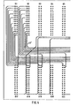
- FIG. 3 shows one of the plug-in modules G1 to G16. It consists of a printed circuit board LP which bears the sub-switching matrix consisting of 256 switching points KP arranged in a 16x16 matrix, a first connector strip S1 and a second connector strip S2.
- the printed circuit board LP has conductor tracks LB which connect the coupling points KP to one another and the 16 inputs E1 to E16 and the 16 outputs A1 to A16 of the sub-switching matrix to the plug strips S1 and S2.
- the inputs E1 to E16 are all on the first connector S1, the outputs A1 to A16 are all led out on the second connector S2.
- the first connector strip S1 is closest to the first magazine M1. Therefore, the inputs E1 to E16 are brought out on it, because they have to be connected to the outputs of the first magazine M1 according to FIG. The same applies analogously to the second connector afford S2 and for the plug-in modules of the other magazines.
- the conductor tracks LB were shown here as single-pole. However, since switching matrixes are usually made with two or even four wires, you have to imagine two or four conductor tracks instead of a line and a corresponding number of connector pins on the connector strips.
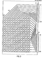
- FIGS. 4 and 6 one of the backplane circuit boards L1 and L2 is shown. Place these figures next to each other, Figure 4 on the left and Figure 6 on the right. The respective upper and lower lines and the left and right lines on FIGS. 4 and 6 indicate the outlines of this backplane.
- B1 to B16 (top row) and B17 to B32 denote the locations for the socket strips B1 to B32. These socket strips themselves are not shown, but only the pads for their soldering pins are indicated by dots.
- the outputs A1 to A16 of the plug-in modules G1 to G16 from the first magazine M1 lie on the socket strips B1 to B16, as can be seen from FIGS. 2 and 3.
- the inputs E1 to E16 of the plug-in modules of the second magazine M2 are located on the socket strips B17 to B32, starting at the top with E1 and A1.
- connections to be created according to Table 1 are formed by conductor tracks LB '.
- a single-pole display was chosen here again; and one has to imagine two conductor tracks instead of a line, since, as can be seen from the representation of two pads for each input and output, here a backplane for a two-wire switching matrix is drawn. Only a few of the many connections to be created according to Table 1 are shown here. In addition, it is not shown that the conductor tracks are distributed over different levels of a multilayer board in order to accommodate their large number and to be able to cross them.
- the second backplane is designed like the first, since according to Table 1 the scheme of the connections between the first and the second stage is the same as that of the connections between the second and third stages.
- the connections produced in this way have electrical properties (e.g. crosstalk attenuation) with little manufacturing variation, and as a result the connections are also suitable for transmitting higher-frequency message signals.
- electrical properties e.g. crosstalk attenuation
- the possible mechanical manufacturing processes of such printed circuit boards also rule out errors due to human error.
- FIG. 7 shows a section through a multilayer plate in order to show the position of the conductor tracks in it. It has nine layers, between which the hatched conductor tracks lie.
- a two-wire switching matrix is assumed, i.e. each connection is designed as a pair of conductor tracks.
- the first pair is labeled LB1 and lies on the first level between the first and second layers.
- the second pair LB2 is not arranged in the next level immediately next to the first pair LB1, but is laterally offset in accordance with the crosstalk attenuation requirement. This transfer extends over four levels.
- the given crosstalk attenuation requirements only make it possible to arrange a pair LB3 again in the fifth level without displacement relative to the first pair LB1.
- the construction system according to the invention is particularly well suited for the construction of broadband switching networks in broadband communication systems in which, among other things, digitized television signals are transmitted at high bit rates. Due to the further development according to claim 2, it is also suitable for communication systems with bit rates of 140 Mbit / s.
- the plug-in modules and magazines of the assembly system according to the invention can be produced from the standardized and commercially available parts of the Intermas assembly system, so that no special designs are required.
- the production of the backplane circuit boards does not pose any new problems either, since they are no larger than those that are common in the Intermas assembly system.
Landscapes
- Engineering & Computer Science (AREA)
- Microelectronics & Electronic Packaging (AREA)
- Physics & Mathematics (AREA)
- Electromagnetism (AREA)
- Computer Networks & Wireless Communication (AREA)
- Details Of Connecting Devices For Male And Female Coupling (AREA)
- Electrotherapy Devices (AREA)
- Organic Insulating Materials (AREA)
- Structure Of Telephone Exchanges (AREA)
- Coupling Device And Connection With Printed Circuit (AREA)
- Metal-Oxide And Bipolar Metal-Oxide Semiconductor Integrated Circuits (AREA)
Abstract
Description
- Die Erfindung betrifft ein Aufbausystem für Geräte der elektrischen Nachrichtentechnik gemäß dem Oberbegriff des Patentanspruches 1. Ein solches Aufbausystem ist aus der deutschen Gebrauchsmusterschrift 72 15 350 bekannt. Es besteht aus Steckbaugruppen, welche elektrische Bauelemente und an 'einer Kante Steckerleisten tragen. Mehrere Steckbaugruppen werden von vorne in ein Magazin eingesteckt, welches an seiner Rückseite eine Rückwandleiterplatte trägt. Diese trägt Buchsenleisten, in die die Steckerleisten eingreifen. Die Buchsenleisten sind elektrisch untereinander mittels Leiterbahnen der Rückwandleiterplatte verbunden. Größere Geräte bestehen aus mehreren solchen Magazinen, die elektrisch untereinander durch Kabelbäume verbunden sind. Diese Kabelbäume werden in personalaufwendiger Handarbeit hergestellt, wobei sich Fehler einschleichen können. Wegen dieser Handarbeit ist ferner die Lage der einzelnen Drähte in den Kabelbäumen von Exemplar zu Exemplar unterschiedlich. Das hat zur Folge, daß ihre elektrischen Eigenschaften, besonders die Nebensprechdämpfung zwischen zwei Drähten oder Drahtpaaren, ebenfalls unterschiedlich und nicht vorhersehbar ist. Dies schränkt die Verwendbarkeit von Kabelbäumen bei Nachrichtensignalen mit höheren Frequenzen ein.
- Bei vielen Geräten sind zwischen den einzelnen Magazinen eine sehr große Zahl von Verbindungen nötig, wobei diese auf dem einen Magazin in einer bestimmten Ordnung entspringen, jedoch auf dem anderen Magazin in einer völlig anderen Ordnung enden. Dies wird anhand der Figur 1 verdeutlicht.
- Die Figur 1 zeigt als Übersichtsplan ein dreistufiges Koppelfeld für eine Nachrichtenvermittlungsanlage. Jede Stufe besteht aus 16 Teilkoppelfeldern. Für die Verwirklichung eines solchen Koppelfeldes bietet sich das zuvor beschriebene Aufbausystem an. So wird man die Teilkoppelfelder als Steckbaugruppen ausbilden und diese nach Stufen geordnet in Magazine unterbringen. So ergeben sich im Beispiel der Figur 1 je Stufe 16 Steckbaugruppen G1 bis G16 mit je einem Teilkoppelfeld. Jedes Teilkoppelfeld besteht aus 256, in einer 16x16-Matrix angeordnete Koppelpunkte KP.
- Die jeweils 16 Teilkoppelfelder, also die 16 Steckbaugruppen G1 bis G16 einer Stufe sind in einem eigenen Magazin untergebracht, die der ersten Stufe in einem ersten Magazin M1, die der zweiten Stufe in einem zweiten Magazin M2 und die der dritten Stufe in einem dritten Magazin M3.
- Jede Steckbaugruppe weist 16 Eingänge E1 bis E16 und 16 Ausgänge A1 bis A16 auf. Da diese Ein- und Ausgänge auch alle aus dem jeweiligen Magazin herausgeführt sind, weist jedes Magazin, also jede Stufe, 256 Eingänge und 256 Ausgänge auf. In nicht dargestellter Weise sind die 256 Eingänge der ersten Stufe mit 256 Nachrichtenquellen und die 256 Ausgänge der dritten Stufe mit 256 Nachrichtensenken verbunden. Die 256 Ausgänge der ersten Stufe sind mit den 256 Eingängen der zweiten Stufe und deren 256 Ausgänge mit den 256 Eingängen der dritten Stufe nach dem in folgender Tabelle 1 angegebenen Schema verbunden:


- a) Es sollen die handelsüblichen mechanischen Teile wie Magazine, Steckbaugruppen, Stecker- und Buchsenleisten verwendet werden können, z.B. die aus dem Intermas-Aufbausystem.
- b) Die elektrischen Verbindungen zwischen zwei benachbarten Magazinen sollen so gestaltet sein, daß folgende Bedingungen erfüllt sind:
- b1) Fehlerfreie und wenig personalaufwendige Herstellung.
- b2) Geeignet für eine Vielzahl von einzelnen Verbindungen.
- b3) Die Verbindungen können auf den Magazinen in unterschiedlichen Ordnungen entspringen bzw. enden. Es soll nicht nur das in der Tabelle 1 angegebene Schema sondern jedes beliebige verwirklicht werden können.
- b4) Geringe Exemplarsteuerungen der elektrischen Eigenschaften.
- Diese Aufgabe wird durch die im Kennzeichen des Anspruchs 1 genannten Merkmale gelöst. Durch die Weiterbildung nach dem Anspruch 2 wird das Aufbausystem für die Übertragung von Datensignalen mit einer Bitrate bis zu 150 MBit/s ausgestaltet.
- Das zuvor erwähnte Intermas-Aufbausystem ist in der deutschen Zeitschrift "Technische Mitteilungen AEG-TELEFUNKEN" 62. Jg. (1972) H. 4/5, S. 148 bis 162 beschrieben. Aus genormten Teilen lassen sich Steckbaugruppen (dort Baugruppen oder steckbare Leiterplatten genannt) aufbauen, die sich in ebenfalls genormte Magazine (dort Volleinsätze genannt) einschieben lassen.
- Ein dreistufiges Koppelfeld ist in der europäischen Patentschrift 0 037 882 beschrieben. Es erfordert Leiterplatten, welche um 90° verdreht mit ihren Stirnseiten aneinander stoßen. Über irgendeine Halterung dieser Leiterplatten und ihre Unterbringung in ein Magazin lehrt diese Schrift nichts. Es scheint eine Spezialkonstruktion notwendig zu sein. Außerdem können die Verbindungen zwischen den einzelnen Stufen nicht beliebig geführt werden. Mit diesem bekannten mehrstufigen Koppelfeld lassen sich also die dieser Erfindung zu Grunde liegenden Teilaufgaben a) und b3) nicht lösen.
- Die Erfindung wird anhand eines in den Figuren 2 bis 7 dargestellten Ausführungsbeispiels beschrieben, wobei die Figuren 2 bis 6 den Patentanspruch 1 betreffen und wobei anhand der Figur 7 ein Merkmal des Patentanspruches 2 erläutert wird. Dieses Ausführungsbeispiel zeigt, wie das in der Figur 1 gezeigte Koppelfeld durch das erfindungsgemäße Aufbausystem in vorteilhafter Weise aufgebaut werden kann. Die Figur 2 zeigt wieder die drei Magazine M1 bis M3, und zwar hier ihre mechanische Anordnung übereinander. Das erste Magazin M1 befindet sich oben, darunter ist das zweite Magazin M2 und ganz unten das dritte Magazin M3 angeordnet. Sie sind in nicht dargestellter Weise mechanisch miteinander verbunden. Das zweite Magazin ist also sowohl dem ersten als auch dem dritten benachbart.
- Jedes Magazin weist oben und unten je 16 Führungsleisten F auf, in die die Steckbaugruppen geführt werden. Es sind nur die unteren Führungsleisten sichtbar. Von den 48 Steckbaugruppen (16 je Magazin) ist nur die sechzehnte Steckbaugruppe G16 des dritten Magazins M3 dargestellt. Jede Steckbaugruppe trägt als Steckverbinder eine erste und eine zweite Steckerleiste S1 bzw. S2.
- Ferner ist eine erste und eine zweite Rückwandleiterplatte L1 bzw. L2 dargestellt. Jede trägt als Gegensteckverbinder zwei Reihen von je 16 Buchsenleisten, wobei die Buchsenleisten B1 bis B16 die obere Reihe und die Buchsenleisten B17 bis B32 die untere Reihe bilden. Die Buchsenleiste B17 und einige weitere, nicht bezeichnete Buchsenleisten sind hier nicht sichtbar. Weiter sind eine dritte und eine vierte Rückwandleiterplatte L3 bzw. L4 vorgesehen. Diese tragen nur eine Reihe von je 16 Buchsenleisten.
- Durch gestrichelte Linien ist angedeutet, in welche der Führungsleisten die dargestellte Steckbaugruppe G16 bei ihrem Einstecken geführt wird, welche Lage die Rückwandleiterplatten an der Rückseite der Magazine nach dem Zusammenbau einnehmen sowie daß die Steckerleisten S1 und S2 der dargestellten Steckbaugruppe G16 in die Buchsenleiste B32 der zweiten Rückwandleiterplatte L2 und in eine nicht bezeichnete Buchsenleiste der vierten Rückwandleiterplatte L4 eingreifen. In der gleichen Weise greifen die Steckerleisten der nicht dargestellten Steckbaugruppen in die ihnen zugeordneten Buchsenleisten ein. So ergibt sich eine Zuordnung gemäß der folgenden Tabelle 2:

- Die Rückwandleiterplatte L1 umfaßt also den Bereich der Stekkerleisten S2 des ersten Magazins M1 und den Bereich der Steckerleisten S1 des zweiten Magazins M2. Der Bereich der Steckerleisten S2 des ersten Magazins M1 ist dem Bereich der Steckerleisten S1 des zweiten Magazins M2 benachbart. Das gleiche gilt sinngemäß für die Rückwandleiterplatte L2.
- In der Figur 3 ist eine der Steckbaugruppen G1 bis G16 dargestellt. Sie besteht aus einer Leiterplatte LP, welche das aus 256, in einer 16x16-Matrix angeordnete Kcppelpunkte KP bestehende Teilkoppelfeld, eine erste Steckerleiste S1 und eine zweite Steckerleiste S2 trägt. Die Leiterplatte LP weist Leiterbahnen LB auf, die die Koppelpunkte KP untereinander sowie die 16 Eingänge E1 bis E16 und die 16 Ausgänge A1 bis A16 des Teilkoppelfeldes mit den Steckerleisten S1 bzw. S2 verbinden. Die Eingänge E1 bis E16 sind alle auf der ersten Steckerleiste S1, die Ausgänge A1 bis A16 sind alle auf der zweiten Steckerleiste S2 herausgeführt. Wie aus der Figur 2 hervorgeht, ist bei den Steckbaugruppen des zweiten Magazins M2 die erste Steckerleiste S1 dem ersten Magazin M1 am nächsten gelegen. Deshalb sind auf ihr die Eingänge E1 bis E16 herausgeführt, weil diese gemäß der Figur 1 mit den Ausgängen des ersten Magazins M1 verbunden werden müssen. Das Gleiche gilt sinngemäß für die zweiten Steckerleisten S2 und für die Steckbaugruppen der anderen Magazine.
- Die Leiterbahnen LB wurden hier einpolig dargestellt. Da Koppelfelder jedoch üblicherweise zwei- oder gar vieradrig ausgeführt werden, muß man sich anstelle einer Linie zwei bzw. vier Leiterbahnen und auf den Steckerleisten entsprechend viele Steckerstifte vorstellen.
- In den Figuren 4, 5 und 6 ist eine der Rückwandleiterplatten L1 bzw. L2 dargestellt. Diese Figuren lege man nebeneinander, die Figur 4 links und die Figur 6 rechts. Die jeweils obere und untere Linie sowie die linke bzw. rechte Linie auf der Figur 4 bzw. 6 geben die Umrisse dieser Rückwandleiterplatte an. Mit B1 bis B16 (obere Reihe) und B17 bis B32 sind die Plätze für die Buchsenleisten B1 bis B32 bezeichnet. Diese Buchsenleisten selbst sind nicht dargestellt, sondern es sind durch Punkte nur die Lötaugen für ihre Lötstifte angedeutet. Betrachtet man die erste Rückwandleiteplatte L1, so liegen, wie aus den Figuren 2 und 3 hervorgeht, auf den Buchsenleisten B1 bis B16 die Ausgänge A1 bis A16 der Steckbaugruppen G1 bis G16 aus dem ersten Magazin M1. Auf den Buchsenleisten B17 bis B32 liegen die Eingänge E1 bis E16 der Steckbaugruppen des zweiten Magazins M2, und zwar jeweils oben mit E1 bzw. A1 beginnend.
- Die Verbindungen, die gemäß der Tabelle 1 zu schaffen sind, werden durch Leiterbahnen LB' gebildet. Dabei wurde hier wieder eine einpolige Darstellung gewählt; und man muß sich anstelle einer Linie zwei Leiterbahnen vorstellen, da, wie an der Darstellung von je zwei Lötaugen für jeden Ein- bzw. Ausgang zu erkennen ist, hier eine Rückwandleiterplatte für ein zweiadriges Koppelfeld gezeichnet ist. Von den vielen, laut Tabelle 1 zu schaffenden Verbindungen sind hier nur einige gezeichnet. Außerdem ist nicht gezeichnet, daß die Leiterbahnen auf verschiedene Ebenen einer Multilayerplatte verteilt sind, um ihre große Zahl unterbringen und ihre Kreuzungen ausführen zu können.
- Um Stoßstellen, die gerade bei höherfrequenten Nachrichtensignalen stören, zu vermeiden, sind spitzwinklige Abknickungen der Leiterbahnen ganz vermieden und rechtwinklige in zwei stumpfwinklige aufgelöst. Statt der Auflösung in stumpfwinklige Abknickungen ist eine abgerundete Ausführung möglich. Dies gilt auch für die Leiterbahnen der Steckbaugruppen. Falls sich spitzwinklige Abknickungen nicht vermeiden lassen, werden sie ebenfalls in mehrere stumpfwinklige aufgelöst oder abgerundet ausgeführt.
- In diesem Ausführungsbeispiel ist die zweite Rückwandleiterplatte wie die erste ausgeführt, da laut Tabelle 1 das Schema der Verbindungen zwischen der ersten u-.d der zweiten Stufe dem der Verbindungen zwischen der zweiten und dritten Stufe gleicht. Es können aber auch ungleiche Schemen verwirklicht werden, es sind nur verschiedene Rückwandleiterplatten mit entsprechend geführten Leiterbahnen vorzusehen.
- Es können auch nur durch entsprechende Führung der Leiterbahnen auf den Rückwandleiterplatten von der Tabelle 1 völlig abweichende Schemen verwirklicht werden.
- Durch Anwendung der Leiterplattentechnik in Form der erfindungsgemäßen Rückwandleiterplatten weisen die so hergestellten Verbindungen elektrische Eigenschaften (z.B. Nebensprechdämpfung) mit geringen Fertigungsstreuungen auf, und dadurch sind die Verbindungen auch zur Übertragung höherfrequenter Nachrichtensignale geeignet. Durch die möglichen maschinellen Herstellungsverfahren solcher Leiterplatten sind ferner Fehler durch menschliche Irrtümer ausgeschlossen.
- Die Darstellung der dritten und vierten Rückeandleiterplat- te L3 und L4 in einer eigenen Figur erübrigt sich, da auf ihnen in herkömmlicher Weise die Verbindungen von den Signalquellen zu den Eingängen der ersten Stufe bzw. von den Ausgängen der dritten Stufe zu den Nachrichtensenken hergestellt werden. Nicht dargestellt sind ferner Schaltmittel und Steuerleitungen zum Durchschalten und Ausschalten der Koppelpunkte. Dies gilt auch für die Steckbaugruppen.
- Die Figur 7 zeigt einen Schnitt durch eine Multilayerplatte, um die Lage der Leiterbahnen in ihr darzustellen. Sie weist neun Schichten auf, zwischen denen die schraffiert gezeichneten Leiterbahnen liegen. Es wird ein zweiadrig aufgebautes Koppelfeld angenommen, d.h., jede Verbindung ist als ein Paar von Leiterbahnen ausgeführt. Das erste Paar ist mit LB1 bezeichnet und liegt in der ersten Ebene zwischen der ersten und zweiten Schicht. Um auch bei höherfrequenten Nachrichtensignalen eine ausreichend hohe Nebensprechdämpfung zu erreichen, ist das zweite Paar LB2 in der nächsten Ebene nicht unmittelbar neben dem ersten Paar LB1 angeordnet, sondern entsprechend der Nebensprechdämpfungsforderung seitlich versetzt. Diese Versetzung erstreckt sich über vier Ebenen. Die gegebenen Nebensprechdämpfungsforderungen erlauben es erst, in der fünften Ebene wieder ein Paar LB3 ohne Versetzung gegenüber dem ersten Paar LB1 anzuordnen.
- Das erfindungsgemäße Aufbausystem ist besonders gut geeignet zum Aufbau von Breitband-Koppelfelder in Breitband-Kommunikationssystemen, in denen u.a. digitalisierte Fernsehsignale mit hohen Bitraten übertragen werden. Durch die Weiterbildung nach dem Anspruch 2 ist es auch für Kommunikationssysteme mit Bitraten von 140 MBit/s geeignet.
- Mit dem erfindungsgemäßen Aufbausystem können jedoch nicht nur mehrstufige Koppelfelder sondern auch andere, aus mehreren Stufen bestehende elektrische Geräte aufgebaut werden, bei denen Steckbaugruppen stufenweise geordnet in Magazinen untergebracht werden und wo zwischen den benachbarten Magazinen viele elektrische Verbindungen notwendig sind.
- Die Steckbaugruppen und Magazine des erfindungsgemäßen Aufbausystems können aus den genormten und handelsüblichen Teilen des Intermas-Aufbausystems hergestellt werden, so daß keine Sonderkonstruktionen erforderlich sind. Auch die Herstellung der Rückwandleiterplatten wirft keine neuen Probleme auf, da sie nicht größer sind als die im Intermas-Aufbausystem üblichen.
Claims (2)
Priority Applications (1)
| Application Number | Priority Date | Filing Date | Title |
|---|---|---|---|
| AT85112837T ATE39398T1 (de) | 1985-01-24 | 1985-10-10 | Aufbausystem fuer geraete der elektrischen nachrichtentechnik. |
Applications Claiming Priority (2)
| Application Number | Priority Date | Filing Date | Title |
|---|---|---|---|
| DE3502295 | 1985-01-24 | ||
| DE19853502295 DE3502295A1 (de) | 1985-01-24 | 1985-01-24 | Aufbausystem fuer geraete der elektrischen nachrichtentechnik |
Publications (2)
| Publication Number | Publication Date |
|---|---|
| EP0191902A1 true EP0191902A1 (de) | 1986-08-27 |
| EP0191902B1 EP0191902B1 (de) | 1988-12-21 |
Family
ID=6260642
Family Applications (1)
| Application Number | Title | Priority Date | Filing Date |
|---|---|---|---|
| EP85112837A Expired EP0191902B1 (de) | 1985-01-24 | 1985-10-10 | Aufbausystem für Geräte der elektrischen Nachrichtentechnik |
Country Status (6)
| Country | Link |
|---|---|
| US (1) | US4679121A (de) |
| EP (1) | EP0191902B1 (de) |
| AT (1) | ATE39398T1 (de) |
| CA (1) | CA1247223A (de) |
| DE (2) | DE3502295A1 (de) |
| DK (1) | DK161276C (de) |
Cited By (2)
| Publication number | Priority date | Publication date | Assignee | Title |
|---|---|---|---|---|
| EP0240580A1 (de) * | 1986-04-03 | 1987-10-14 | ANT Nachrichtentechnik GmbH | Dreistufige Koppelanordnung |
| US4862161A (en) * | 1985-01-24 | 1989-08-29 | Ant Nachrichtentechnik Gmbh | Three-stage coupling arrangement |
Families Citing this family (23)
| Publication number | Priority date | Publication date | Assignee | Title |
|---|---|---|---|---|
| US4742477A (en) * | 1984-08-20 | 1988-05-03 | Sci Systems, Inc. | Computer terminal controller and method |
| US4777615A (en) * | 1986-02-28 | 1988-10-11 | Scientific Computer Systems Corporation | Backplane structure for a computer superpositioning scalar and vector operations |
| US5218519A (en) * | 1987-09-08 | 1993-06-08 | Digital Equipment Corporation | Card cage system |
| DE3733264C1 (de) * | 1987-10-01 | 1989-03-30 | Moestronik Unisel Elektronisch | Elektronische Einrichtung |
| US4918335A (en) * | 1987-11-06 | 1990-04-17 | Ford Aerospace Corporation | Interconnection system for integrated circuit chips |
| WO1989007349A1 (en) * | 1988-02-05 | 1989-08-10 | Commodore-Amiga, Inc. | Universal connector device |
| US4954949A (en) * | 1988-02-05 | 1990-09-04 | Commodore-Amiga, Inc. | Universal connector device for bus networks in host computer/co-processor computer system |
| US5028809A (en) * | 1989-03-07 | 1991-07-02 | Hewlett-Packard Company | Computer bus structure permitting replacement of modules during operation |
| US5243493A (en) * | 1992-04-29 | 1993-09-07 | Industrial Technology Research Institute | Fanless convection cooling design for personal computers |
| US5227957A (en) * | 1992-05-14 | 1993-07-13 | Deters John B | Modular computer system with passive backplane |
| US5483229A (en) * | 1993-02-18 | 1996-01-09 | Yokogawa Electric Corporation | Input-output unit |
| US5442520A (en) * | 1994-07-01 | 1995-08-15 | Cincinnnati Milacron Inc. | Apparatus for printed circuit board connection |
| US5838533A (en) * | 1997-03-19 | 1998-11-17 | Eaton Corporation | Housing assembly for circuit components |
| US5991163A (en) * | 1998-11-12 | 1999-11-23 | Nexabit Networks, Inc. | Electronic circuit board assembly and method of closely stacking boards and cooling the same |
| US11042211B2 (en) | 2009-08-07 | 2021-06-22 | Advanced Processor Architectures, Llc | Serially connected computing nodes in a distributed computing system |
| US9429983B1 (en) | 2013-09-12 | 2016-08-30 | Advanced Processor Architectures, Llc | System clock distribution in a distributed computing environment |
| US9645603B1 (en) | 2013-09-12 | 2017-05-09 | Advanced Processor Architectures, Llc | System clock distribution in a distributed computing environment |
| US8022526B2 (en) | 2009-08-07 | 2011-09-20 | Advanced Processor Architectures, Llc | Distributed computing |
| US8755197B1 (en) * | 2010-12-31 | 2014-06-17 | Veetle, Inc. | High-density, low-power computer cluster for video streaming |
| US9924609B2 (en) * | 2015-07-24 | 2018-03-20 | Transtector Systems, Inc. | Modular protection cabinet with flexible backplane |
| US10356928B2 (en) | 2015-07-24 | 2019-07-16 | Transtector Systems, Inc. | Modular protection cabinet with flexible backplane |
| US10588236B2 (en) * | 2015-07-24 | 2020-03-10 | Transtector Systems, Inc. | Modular protection cabinet with flexible backplane |
| JP7041085B2 (ja) * | 2019-02-05 | 2022-03-23 | ファナック株式会社 | 電子装置 |
Citations (6)
| Publication number | Priority date | Publication date | Assignee | Title |
|---|---|---|---|---|
| US3798762A (en) * | 1972-08-14 | 1974-03-26 | Us Army | Circuit board processing |
| US3808505A (en) * | 1973-03-19 | 1974-04-30 | Gte Automatic Electric Lab Inc | Apparatus for interconnecting a plurality of electronic equipment frames |
| DE2304456A1 (de) * | 1973-01-30 | 1974-08-01 | Siemens Ag | Einschubsystem fuer elektronikbaugruppen |
| US3923360A (en) * | 1973-03-26 | 1975-12-02 | Cii Honeywell Bull | Multilayer electrical connection panel with modifiable internal circuits |
| US4016463A (en) * | 1973-10-17 | 1977-04-05 | Amdahl Corporation | High density multilayer printed circuit card assembly and method |
| DE2615642A1 (de) * | 1976-04-08 | 1977-10-20 | Licentia Gmbh | Einschub |
Family Cites Families (8)
| Publication number | Priority date | Publication date | Assignee | Title |
|---|---|---|---|---|
| GB806835A (en) * | 1955-03-31 | 1958-12-31 | Standard Telephones Cables Ltd | Improvements in or relating to electronic equipment practice |
| US3179904A (en) * | 1962-12-05 | 1965-04-20 | Ibm | Flexible multiconductor transmission line utilizing alternate conductors as crosstalk shields |
| US3715629A (en) * | 1967-04-05 | 1973-02-06 | Amp Inc | Wiring device for interconnecting module circuit units |
| US3539873A (en) * | 1967-10-19 | 1970-11-10 | Clare & Co C P | Matrix board apparatus |
| US3623127A (en) * | 1969-11-03 | 1971-11-23 | Ashley C Glenn | Electrical printed circuit switching device |
| DE7215350U (de) * | 1972-04-21 | 1972-07-27 | Siemens Ag | Aufnahmevorrichtung für Steckbaugruppen |
| DE3165314D1 (en) * | 1980-04-14 | 1984-09-13 | Grundig Emv | Multi-stage coupling field |
| SE423777B (sv) * | 1980-09-29 | 1982-05-24 | Asea Ab | Elektrisk utrustning innefattande ett antal samarbetande kretskort |
-
1985
- 1985-01-24 DE DE19853502295 patent/DE3502295A1/de not_active Withdrawn
- 1985-10-10 DE DE8585112837T patent/DE3566941D1/de not_active Expired
- 1985-10-10 EP EP85112837A patent/EP0191902B1/de not_active Expired
- 1985-10-10 AT AT85112837T patent/ATE39398T1/de active
-
1986
- 1986-01-22 CA CA000500104A patent/CA1247223A/en not_active Expired
- 1986-01-23 DK DK034686A patent/DK161276C/da active
- 1986-01-24 US US06/864,418 patent/US4679121A/en not_active Expired - Lifetime
Patent Citations (6)
| Publication number | Priority date | Publication date | Assignee | Title |
|---|---|---|---|---|
| US3798762A (en) * | 1972-08-14 | 1974-03-26 | Us Army | Circuit board processing |
| DE2304456A1 (de) * | 1973-01-30 | 1974-08-01 | Siemens Ag | Einschubsystem fuer elektronikbaugruppen |
| US3808505A (en) * | 1973-03-19 | 1974-04-30 | Gte Automatic Electric Lab Inc | Apparatus for interconnecting a plurality of electronic equipment frames |
| US3923360A (en) * | 1973-03-26 | 1975-12-02 | Cii Honeywell Bull | Multilayer electrical connection panel with modifiable internal circuits |
| US4016463A (en) * | 1973-10-17 | 1977-04-05 | Amdahl Corporation | High density multilayer printed circuit card assembly and method |
| DE2615642A1 (de) * | 1976-04-08 | 1977-10-20 | Licentia Gmbh | Einschub |
Non-Patent Citations (1)
| Title |
|---|
| ELONCO BULLETIN, Nr. 68, September 1971, Seiten 2-13,, Philips, Eindhoven, NL; "Moderne verbindingstechnieken" * |
Cited By (2)
| Publication number | Priority date | Publication date | Assignee | Title |
|---|---|---|---|---|
| US4862161A (en) * | 1985-01-24 | 1989-08-29 | Ant Nachrichtentechnik Gmbh | Three-stage coupling arrangement |
| EP0240580A1 (de) * | 1986-04-03 | 1987-10-14 | ANT Nachrichtentechnik GmbH | Dreistufige Koppelanordnung |
Also Published As
| Publication number | Publication date |
|---|---|
| DE3502295A1 (de) | 1986-07-24 |
| DK34686A (da) | 1986-07-25 |
| DK161276B (da) | 1991-06-17 |
| EP0191902B1 (de) | 1988-12-21 |
| US4679121A (en) | 1987-07-07 |
| DE3566941D1 (en) | 1989-01-26 |
| DK161276C (da) | 1991-12-09 |
| ATE39398T1 (de) | 1989-01-15 |
| CA1247223A (en) | 1988-12-20 |
| DK34686D0 (da) | 1986-01-23 |
Similar Documents
| Publication | Publication Date | Title |
|---|---|---|
| EP0191902B1 (de) | Aufbausystem für Geräte der elektrischen Nachrichtentechnik | |
| EP0712267B1 (de) | Modulare Steuerungsanlage mit integriertem Feldbusanschluss | |
| DE3740568C2 (de) | ||
| DE69214289T2 (de) | Elektrisches verbindungssystem | |
| DE2432441A1 (de) | Kreuzverbindungsschalter | |
| DE2130637A1 (de) | Elektronischer Baustein und aus mehreren solcher Bausteine gebildete Schaltungsanordnung | |
| DE2349444A1 (de) | Steckkontaktschalter | |
| DE3836360A1 (de) | Verteilereinrichtung, insbesondere fuer den hauptverteiler von fernsprechanlagen | |
| EP3562283A1 (de) | Modulare backplaneanordnung | |
| EP0222030A1 (de) | Initiatorklemmenblock | |
| DE3511344A1 (de) | Steckverbinder fuer rueckwandverdrahtungen | |
| DE2644296A1 (de) | Dreireihiger leitungsstecker mit sogenannten kontaktgabeln zum anschliessen von flachbandkabeln | |
| DE2214503A1 (de) | Aufnahmevorrichtung zur aufnahme von gehaeusen fuer die elektrische nachrichtenuebertragungstechnik | |
| EP0270185B1 (de) | Breitband-Raumvielfachkoppelfeld mit Zwischenleitungsführung in einer Leiterplatte mit mehrlagigen Leiterbahnen in Mikrostrip-Technik | |
| EP0240580B2 (de) | Dreistufige Koppelanordnung | |
| DE2901678B1 (de) | Verteiler fuer kleine Fernsprechvermittlungsanlagen | |
| DE3736025C1 (en) | Multiple plug connector | |
| DE3249507T1 (de) | Reihen- oder schichtenweise angeordnete, senkrecht zueinander in Bezug stehende, drei dimensionale gedruckte Plattenschaltung | |
| EP1503307A1 (de) | Vorrichtung zur Emulation von Entwürfen für integrierte Schaltkreise | |
| DE8908973U1 (de) | Eine aus mindestens aus zwei parallel zueinander angeordneten Leiterplatten bestehende Baugruppe mit elektrisch leitender Verbindung | |
| EP0199309A2 (de) | Vielfachschaltelement zum Verbinden einer Mehrzahl von Mehrfachbussen | |
| DE3435773A1 (de) | Rueckwandverdrahtung fuer einschiebbare elektrische baugruppen | |
| DE2247523A1 (de) | Elektrische oder elektronische koppelanordnung fuer fernmelde-, insbesondere fernsprechvermittlungsanlagen | |
| EP0865121A1 (de) | Stecker-Adapter zum Verbinden eines vierpoligen Steckverbinders mit einem achtpoligen Steckverbinder nach RJ45 Norm | |
| WO2016162017A1 (de) | Steckermodul für einen modularen steckverbinder |
Legal Events
| Date | Code | Title | Description |
|---|---|---|---|
| PUAI | Public reference made under article 153(3) epc to a published international application that has entered the european phase |
Free format text: ORIGINAL CODE: 0009012 |
|
| AK | Designated contracting states |
Kind code of ref document: A1 Designated state(s): AT BE DE FR GB IT NL SE |
|
| 17P | Request for examination filed |
Effective date: 19860911 |
|
| 17Q | First examination report despatched |
Effective date: 19880504 |
|
| GRAA | (expected) grant |
Free format text: ORIGINAL CODE: 0009210 |
|
| AK | Designated contracting states |
Kind code of ref document: B1 Designated state(s): AT BE DE FR GB IT NL SE |
|
| ITF | It: translation for a ep patent filed | ||
| REF | Corresponds to: |
Ref document number: 39398 Country of ref document: AT Date of ref document: 19890115 Kind code of ref document: T |
|
| GBT | Gb: translation of ep patent filed (gb section 77(6)(a)/1977) | ||
| REF | Corresponds to: |
Ref document number: 3566941 Country of ref document: DE Date of ref document: 19890126 |
|
| ET | Fr: translation filed | ||
| PLBE | No opposition filed within time limit |
Free format text: ORIGINAL CODE: 0009261 |
|
| STAA | Information on the status of an ep patent application or granted ep patent |
Free format text: STATUS: NO OPPOSITION FILED WITHIN TIME LIMIT |
|
| 26N | No opposition filed | ||
| ITTA | It: last paid annual fee | ||
| PGFP | Annual fee paid to national office [announced via postgrant information from national office to epo] |
Ref country code: NL Payment date: 19931031 Year of fee payment: 9 |
|
| EAL | Se: european patent in force in sweden |
Ref document number: 85112837.1 |
|
| PG25 | Lapsed in a contracting state [announced via postgrant information from national office to epo] |
Ref country code: NL Effective date: 19950501 |
|
| NLV4 | Nl: lapsed or anulled due to non-payment of the annual fee | ||
| PGFP | Annual fee paid to national office [announced via postgrant information from national office to epo] |
Ref country code: GB Payment date: 20000927 Year of fee payment: 16 |
|
| PGFP | Annual fee paid to national office [announced via postgrant information from national office to epo] |
Ref country code: SE Payment date: 20001009 Year of fee payment: 16 |
|
| PGFP | Annual fee paid to national office [announced via postgrant information from national office to epo] |
Ref country code: FR Payment date: 20001010 Year of fee payment: 16 |
|
| PGFP | Annual fee paid to national office [announced via postgrant information from national office to epo] |
Ref country code: AT Payment date: 20001011 Year of fee payment: 16 |
|
| PGFP | Annual fee paid to national office [announced via postgrant information from national office to epo] |
Ref country code: BE Payment date: 20001214 Year of fee payment: 16 |
|
| PG25 | Lapsed in a contracting state [announced via postgrant information from national office to epo] |
Ref country code: GB Free format text: LAPSE BECAUSE OF NON-PAYMENT OF DUE FEES Effective date: 20011010 Ref country code: AT Free format text: LAPSE BECAUSE OF NON-PAYMENT OF DUE FEES Effective date: 20011010 |
|
| PG25 | Lapsed in a contracting state [announced via postgrant information from national office to epo] |
Ref country code: SE Free format text: LAPSE BECAUSE OF NON-PAYMENT OF DUE FEES Effective date: 20011011 |
|
| PGFP | Annual fee paid to national office [announced via postgrant information from national office to epo] |
Ref country code: DE Payment date: 20011022 Year of fee payment: 17 |
|
| PG25 | Lapsed in a contracting state [announced via postgrant information from national office to epo] |
Ref country code: BE Free format text: LAPSE BECAUSE OF NON-PAYMENT OF DUE FEES Effective date: 20011031 |
|
| REG | Reference to a national code |
Ref country code: GB Ref legal event code: IF02 |
|
| BERE | Be: lapsed |
Owner name: ANT NACHRICHTENTECHNIK G.M.B.H. Effective date: 20011031 |
|
| GBPC | Gb: european patent ceased through non-payment of renewal fee |
Effective date: 20011010 |
|
| EUG | Se: european patent has lapsed |
Ref document number: 85112837.1 |
|
| PG25 | Lapsed in a contracting state [announced via postgrant information from national office to epo] |
Ref country code: FR Free format text: LAPSE BECAUSE OF NON-PAYMENT OF DUE FEES Effective date: 20020628 |
|
| REG | Reference to a national code |
Ref country code: FR Ref legal event code: ST |
|
| PG25 | Lapsed in a contracting state [announced via postgrant information from national office to epo] |
Ref country code: DE Free format text: LAPSE BECAUSE OF NON-PAYMENT OF DUE FEES Effective date: 20030501 |