EP0190973A2 - Abtast- und Halteschaltung - Google Patents
Abtast- und Halteschaltung Download PDFInfo
- Publication number
- EP0190973A2 EP0190973A2 EP86400217A EP86400217A EP0190973A2 EP 0190973 A2 EP0190973 A2 EP 0190973A2 EP 86400217 A EP86400217 A EP 86400217A EP 86400217 A EP86400217 A EP 86400217A EP 0190973 A2 EP0190973 A2 EP 0190973A2
- Authority
- EP
- European Patent Office
- Prior art keywords
- source
- gate
- mos transistor
- terminal
- output
- Prior art date
- Legal status (The legal status is an assumption and is not a legal conclusion. Google has not performed a legal analysis and makes no representation as to the accuracy of the status listed.)
- Granted
Links
Images


Classifications
-
- G—PHYSICS
- G11—INFORMATION STORAGE
- G11C—STATIC STORES
- G11C27/00—Electric analogue stores, e.g. for storing instantaneous values
- G11C27/02—Sample-and-hold arrangements
- G11C27/024—Sample-and-hold arrangements using a capacitive memory element
Definitions
- the present invention relates to a sample-and-hold circuit adapted for a video signal or the like having a blanking period per predetermined cycle, and more particularly to an improved circuit so designed as to produce an output signal without any difference relative to the gate-source offset voltage induced by a buffer of a source follower or the like.
- a signal received at an input terminal 201 is fed to a gating MOS transistor 208 which is turned on by a sampling pulse fed thereto from a terminal 203.
- the output signal of the MOS transistor 208 is fed to a holding capacitor 211, which then produces a signal fed to the gate of a buffer MOS transistor 209.
- a line voltage is applied through a power terminal 205 to the drain of the MOS transistor 209, whose source is grounded via a constant current source 213.
- the signal produced at the source of the MOS transistor 209 is fed to an output terminal 206.
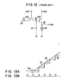
- a buffer circuit composed of a source follower is provided in the output stage. Accordingly, when sampling pulses of Fig; 13B are fed from the terminal 203, signals obtained in the individual stages become such as shown in Fig. 13A.
- a solid line represents the waveform of an input voltage applied to the input terminal 201 point );
- a one-dot chain line represents the waveform of a voltage at the gate (point ) of the MOS transistor 209; and
- a broken line represents the waveform of an output voltage produced at the output terminal 206 (point ).
- V GS offset voltage
- V th is a threshold voltage of the MOS transistor 209
- P is a mobility of a carrier
- C ox is a gate capacity per unit area
- W is a channel width
- L is a channel length
- I o is a current value of the constant current supply 213.
- Fig. 14 In an attempt to eliminate such disadvantages, an improved circuit configuration of Fig. 14 has already been proposed by the present applicant.
- an input terminal 221 In the circuit of Fig. 14, there are shown an input terminal 221, a terminal 223 to be fed with a blanking pulse ⁇ BLK, and a terminal 224 to be fed with a sampling pulse Ws.
- a drain of a gating MOS transistor 227 is connected to the input terminal 221, and a gate thereof is connected to the terminal 224. Meanwhile a source of the MOS transistor 227 is connected via a capacitor 231 to a gate of an enhancement-type output MOS transistor 229 while being grounded via a capacitor 232 and is further connected to a drain of a gating MOS transistor 230.
- a drain of another gating MOS transistor 228 is connected to the input terminal 221, while a gate and a source thereof are connected respectively to the terminal 223 and the gate of the transistor 229.
- the gate of the gating MOS transistor 230 is connected to the terminal 223, and its source is connected to the source of the enhancement-type output MOS transistor 229, whose drain is connected to a power terminal 225. And a constant current supply 233 is connected to the source of the MOS transistor 229, which is led out to an output terminal 226.
- the MOS transistors 228 and 230 are turned off in the state described above, and a sampling pulse ⁇ S is fed.
- the potential at the input terminal 121 is V S1 when a first sampling pulse ⁇ S1 is fed
- the potential V S1 is obtained also at the junction of the transistor 227 and the capacitor 232. Since the charge corresponding to the aforesaid potential difference V GS is previously stored in the capacitor 231 in response to the blanking pulse ⁇ BLR, the potential at the junction of the capacitor 231 and the transistor 229 is increased to be V S1 + V GS . As a result, the potential at the output terminal 126 becomes which is equal to the potential at the input terminal 221.
- the above operation is performed at each sampling time and therefore enables the sampled potential to appear at the output without any variation despite the drop of V GS induced by the buffer.
- the input signal level needs to be higher than at least the threshold voltage Vt h of the MOS transistor 229. Accordingly the dynamic range of the circuit is required to be D l which is greater than the essential signal dynamic range (e.g. D 0 ) by a value corresponding to the offset voltage V GS .
- an input capacity C IN is generated alternatingly in the output-stage MOS transistor 229 as viewed from the input signal source. Consequently the output from the source of the MOS transistor 229 is produced with a delay, and there exists another problem that the power consumption increases with charge and discharge of the input capacity C IN .
- Another object of the present invention is to provide an improved sample-and-hold circuit which is capable of reducing the input capacity of the buffer MOS transistor as viewed from the input signal source.
- an input signal is fed via a first gate element to one end of a first capacitor whose other end is grounded alternatingly, the one end of the first capacitor being connected via a second capacitor to a gate (or base) of a source (or emitter) follower transistor to obtain an output from the source (or emitter) of the source follower transistor which is connected via a second gate element to one end of the first capacitor, while the gate (or base) of the source follower transistor is connected via a third gate element to a DC voltage supply having a predetermined voltage value, and the second and third gate elements are turned on during a first period of the input signal so that a voltage corresponding to the gate-source (or base-emitter) offset voltage of the source follower transistor is stored in the second capacitor, while the first gate element is turned on during a second period of the input signal to reduce an output signal equivalent in level to the input signal.
- Fig. 1 shown at 1 is an input terminal to which a video signal or the like is fed.
- the drain of a gating MOS transistor 7 is connected to the input terminal 1, and the gate thereof is connected to a terminal 4 to be fed with a sampling pulse ⁇ 5.
- the source of the MOS transistor 7 is connected via a capacitor 11 to the gate of an enhancement-type output MOS transistor 9, and the junction between the source of the MOS transistor 7 and the capacitor 11 is grounded via a capacitor 12 while being connected to the drain of a gating MOS transistor 10.
- the drain of a gating MOS transistor 8 is connected to a terminal 2 to which the bias voltage V B is applied, and the gate thereof is connected to a terminal 3 to be fed with a blanking pulse $ BLK . Meanwhile the source of the MOS transistor 8 is connected to the gate of the output MOS transistor 9. The gate of the gating MOS transistor 10 is connected to the terminal 3 to be fed with a blanking pulse ⁇ BLK , and the source thereof is connected to the source of the MOS transistor 9.
- the drain of the output MOS transistor 9 is connected to a power terminal 5 while a constant current supply 13 is connected to the source thereof, from which an output terminal 6 is led out.
- the terminal 2 is fed with a predetermined bias voltage V B substantially equivalent to the mean level of the input signal, and the terminal 3 is fed with a blanking pulse ⁇ BLK of Fig. 2B while the terminal 4 is fed with a sampling pulse ⁇ S of Fig. 2C.
- the MOS transistors 8 and 10 are turned off in the state described above, and then a sampling pulse ⁇ S is fed.
- the potential at the input terminal 1 (point ) is V S1 when a first sampling pulse ⁇ S1 is fed
- the potential V S1 is obtained also at the point . Since the charge corresponding to the aforesaid potential difference V GS is previously stored in the capacitor 11 between the points 4 and 2 in response to the blanking pulse ⁇ BLK , the potential at the point is increased to be V S1 + V GS . As a result, the potential at the point 3 becomes which is equal to the potential at the input terminal 1 (point ).
- the above operation is performed at each sampling time and therefore enables the sampled potential to appear at the output without any variation despite the drop of V GS induced by the buffer.
- a pulse held at a high level as shown in Fig. 3B is fed to the terminal 4 in relation to an input video signal of Fig. 3A.
- the configuration may be so designed that the offset voltage V GS of the MOS transistor 9 is stored in the capacitor 11 in response to a blanking pulse of Fig. 3C fed per blanking period of the video signal.
- Fig. 4 shows another embodiment of the present invention applied to an analog delay circuit, in which two of the foregoing embodiment of Fig. 1 are arrayed in cascade connection.
- a first sample-and-hold circuit comprises gating MOS transistors 27, 28 and 30; capacitors 31 and 32; an output MOS transistor 29 and a constant current supply 33 similarly to the aforesaid exemplary embodiment.
- a second sample-and-hold circuit comprises gating MOS transistors 37, 38 and 40; capacitors 41 and 42; an output MOS transistor 39 and a constant current supply 43 similarly to the above.
- an input terminal 21 is connected to the drain of the MOS transistor 27, whose gate is connected to a terminal 24 to be fed with a first sampling pulse ⁇ S1 .
- a terminal 22, to which a bias voltage V B is applied, is connected to the respective drains of the MOS transistors 28 and 38, while a terminal 23 to be fed with a blanking pulse 4 BLK is connected to the respective gates of the mos transistors 28, 30 and 40.
- the source of the output MOS transistor 29 is connected to the drain of the MOS transistor 37, whose gate is connected to a terminal 34 to be fed with a second sampling pulse ⁇ S2 .
- a power terminal 25 is connected to the respective drains of the output MOS transistors 29 and 39, and an output terminal 36 is led out from the source of the output MOS transistor 39.
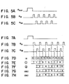
- a blanking pulse 6 BLK of Fig. 5A is fed to the terminal 23, and offset voltages V GS of the output MOS transistors 29 and 39 are stored respectively in the capacitors 31 and 41.
- a first sampling pulse ⁇ S1 of Fig. 5B an input signal is sampled and held to appear as an output at the source of the MOS transistor 29. The output thus produced is then fed to the drain of the MOS transistor 37.
- a second sampling pulse ⁇ S2 of Fig. 5C having a predetermined phase lag with respect to the first sampling pulse ⁇ S1 is fed to a terminal 34, the output of the preceding stage is sampled in response to the second sampling pulse ⁇ S2 . Consequently an output delayed for the phase lag between the second sampling pulse ⁇ S2 and the first sampling pulse ⁇ S1 is obtained at an output terminal 36.
- Fig. 6 shows another embodiment of the present invention applied to an analog serial-parallel conversion circuit, in which two of the foregoing embodiment shown in Fig. 4 are connected in parallel with each other.
- a first delay circuit comprises gating MOS transistors 57, 58, 60, 67, 68 and 70; capacitors 61, 62, 71 and 72; output MOS transistors 59 and 69; and constant current supplies 63 and 73 in the same configuration as that of Fig. 4.
- a second delay circuit comprises gating MOS transistors 77, 78, 80, 87, 88 and 90; capacitors 81, 82, 91 and 92; output MOS transistors 79 and 89; and constant current supplies 83 and 93 in the same configuration as that of Fig. 4.
- an input terminal 51 is connected to the respective drains of the MOS transistors 57 and 77, and the gate of the MOS transistor 57 is connected to a terminal 54 to be fed with a first sampling pulse ⁇ S1 .
- a terminal 52 to which a bias voltage V B is applied, is connected to the respective drains of the MOS transistors 58 and 68, while a terminal 53 to be fed with a blanking pulse ⁇ BLK is connected to the respective gates of the MOS transistors 58, 60, 68 and 70.
- a power terminal 55 is connected to the respective drains of the output MOS transistors 59 and 69.
- a first output terminal 66 is led out from the source of the output MOS transistor 69.
- a terminal 74 to be fed with a second sampling pulse d S2 is connected to the respective gates of the MOS transistors 67 77 and 87.
- a terminal 76, to which a bias voltage V B is applied, is connected to the respective drains of the MOS transistors 78 and 88, while a terminal 53 to be fed with a blanking pulse ⁇ BLK is connected to the respective gates of the MOS transistors 78, 80, 88 and 90.
- a power terminal 75 is connected to the respective drains of the output MOS transistors 79 and 89.
- a second output terminal 86 is led out from the source of the output MOS transistor 89.
- a blanking pulse ⁇ BLK of Fig. 7A is fed to the terminal 53, and offset voltages V GS of the output MOS transistors 59, 69, 79 and 89 are stored respectively in the capacitors 61, 71, 81 and 91.
- a first sampling pulse ⁇ S1 of Fig. 7B an input signal (Fig. 7D) is sampled and held to appear as an output at the source (point in Fig. 6) of the MOS transistor 59.
- the output (Fig. 7E) thus produced is then fed to the drain of the MOS transistor 67.
- the input signal at this moment is sampled in response to the sampling pulse ⁇ S2 , so that an output (Fig. 7F) comes to appear at the source (point in Fig. 6) of the MOS transistor 79.
- the output (Fig. 7F) thus produced is sent via the MOS transistors 87 and 89 to the output terminal 86. That is, the input signal rendered parallel as shown in Figs. 7G and 7H is obtained from the output terminals 66 and 86.
- FIG. 8 shown at 101 is an input terminal to which a video signal or the like is fed.
- the drain of a gating MOS transistor 107 is connected to the input terminal 101, and the gate thereof is connected to a terminal 104 to be fed with a sampling pulse ⁇ S .
- the source of the MOS transistor 107 is connected via a capacitor 115 to the gate of an enhancement-type output MOS transistor 111. And the junction between the source of the MOS transistor 107 and the capacitor 115 is grounded via a capacitor 114 while being connected via a capacitor 113 to the gate of a MOS transistor 110.
- MOS transistors 108, 109 and l12 are connected to a terminal 103 to be fed with a blanking pulse ⁇ BLK .
- the drain of the MOS transistor 108 is connected to the input terminal 101, and the source thereof is connected to the gate of the output MOS transistor 111.
- the drain of the MCS transistor 109 is connected to a terminal 102 to which a DC voltage V DC1 is applied, and its source is connected to the gate of the MOS transistor 110.
- the drain of the MOS transistor 112 is connected to the source of the MOS transistor 107, and the source of the MOS transistor 112 is connected to the source of the output MOS transistor 111.
- the drain of the MOS transistor 110 is connected to a power terminal 105, and its source is connected to the drain of the output MOS transistor 111. Meanwhile a constant current supply 116 is connected to the source of the MOS transistor 111, from which an output terminal 106 is led out.
- An input such as a video signal of Fig. 9A is fed to the input terminal 101.
- the minimum level of the video signal or the sync tip level V BLK thereof during the blanking period is so set as to exceed the threshold voltage Vt h of the output MOS transistor 111.
- To the terminal 102 there is applied from a DC voltage supply a voltage V DC1 which is higher than the sync tip level V BLK and hence further higher than the threshold voltage Vt h of the MOS transistor 110.
- the terminal 103 is fed with a blanking pulse ⁇ SLK of Fig. 9B, while the terminal 104 is fed with a sampling pulse ⁇ S of Fig. 9C.
- the potential at the gate (point in Fig. 8) of the output MOS transistor 111 is equalized to the instantaneous potential at the input terminal 101 (point in Fig. 8) to become V BLK .
- the potential at the source (point in Fig. 8) of the output MOS transistor 111 is reduced by the gate-source offset voltage V GS111 as V BLK - V GS111 .
- the potential at the junction (point in Fig. 8) between the MOS transistor 112 and the capacitor 114 is also reduced as VBLK - V GS111 .
- the potential difference between the points 3 and 2 becomes as follows, and a charge corresponding to such potential difference is stored in the capacitor 113. Meanwhile, the potential difference between the points and becomes as follows, and a charge corresponding thereto is stored in the capacitor 115.
- the MOS transistors 108, 109 and 112 are turned off in the state described above, and then a sampling pulse ⁇ S is fed to the terminal 104.
- the MOS transistor 107 is turned on by the sampling pulse ⁇ S , and the potential at the point is equalized to the instantaneous potential at the input terminal 101 (point in Fig. 8) to become V S , for example.
- the charge corresponding to V GS111 is stored in the capacitor 115 between the points and in response to the blanking pulse ⁇ BLK , so that the potential at the point is altered to V S + V GS111 . Accordingly, the potential at the point 6 is changed to Thus, the output voltage equalized to the input voltage applied to the input terminal 101 is obtained from the output terminal 106.
- the above operation is performed at each sampling time and therefore enables the sampled potential to appear at the output without any variation despite the drop of V GS induced by the buffer.
- each of the alternating potential variations at the drain and the source of the output MOS transistor 111 is Vs so that the apparent input capacity C IN as viewed from the input signal source is reduced to nil.
- a positive pilot signal represented by a broken line Pt in Fig. 9A may additionally be provided during the blanking period of the video signal fed to the input terminal 101.
- the pilot signal Pt is inserted in the high-level duration of the blanking pulse ⁇ BLK , and the peak level of the pilot signal Pt is set to be substantially equal to the mean level of the input signal.
- the offset voltage V GS111 at the same operation point as the signal level can be stored in the capacitor 115 in response to the blanking pulse ⁇ BLK .
- the peak level of the pilot signal Pt is substantially equalized to the mean level of the input signal, it is not necessary to set the sync tip level V BLK of the input signal to be higher than the threshold voltage Vt h of the output MOS transistor, hence minimizing the required dynamic range of the circuit.
- an additional terminal may be provided separately from the input terminal 101 to receive a DC voltage equivalent to the mean level of the input signal, and the drain of the MOS transistor 108 may be connected to such terminal instead of the input terminal 101.
- the output MOS transistor 111 of enhancement type employed in the above embodiment of the invention may be of depression type as well, and a bipolar transistor may be used in place of the MOS transistor.
- Fig. 10 shows still further embodiment of the present invention contrived to constitute an analog delay circuit, wherein two of the foregoing embodiment of Fig. 8 are arrayed in cascade connection with a modification that the drain of the MOS transistor 108 is connected not to the input terminal but to an additional terminal provided separately to receive a DC voltage.
- a first sample-and-hold circuit 120 comprises MOS transistors 127, 128, 129, 130 and 132; capacitors 133, 134 and 135; an output MOS transistor 131 and a constant current supply 136.
- a second sample-and-hold circuit 140 comprises MOS transistors 147, 148, 150 and 152; capacitors 153, 154 and 155; an output MOS transistor 151 and a constant current supply 156.
- an input terminal 121 is connected to the drain of the MOS transistor 127, whose gate is connected to a terminal 124 to be fed with a first sampling pulse ⁇ S1 .
- a terminal 122 to which a DC voltage V DC1 is applied, is connected to the respective drains of the MOS transistors 129 and 149, while a terminal 123 to be fed with a blanking pulse ⁇ BLK is connected to the respective gates of the MOS transistors 128, 129, 148 and 149.
- a terminal 137, to which a DC voltage V DC2 is applied, is connected to the respective drains of the MOS transistors 128 and 148.
- a power terminal 125 is connected to the drain of the MOS transistor 130, and the source of the output MOS transistor 131 in the first sample-and-hold circuit 120 is connected to the drain of the MOS transistor 147 in the second sample-and-hold circuit 140.
- the gate of the MOS transistor 147 is connected to a terminal 144 to be fed with a second sampling pulse ⁇ S2 .
- a power terminal 145 is connected to the drain of the MOS transistor 150, and an output terminal 146 is led out from the source of the output MOS transistor 151.
- a video signal is fed to the input terminal 121, and a DC voltage V DC2 substantially equalized to the mean level of the video signal is applied to the terminal 137.
- the voltage at the drain of the output MOS transistor 131 is altered to V S + V DC1 - (V DC2 - V GS111 ) - V GS110 in response to the first sampling pulse ⁇ S1 of Fig. 11B, whereby the input capacity of the output MOS transistor 131 is reduced to nil alternatingly.
- a sample holding output V S in which the offset voltage V GS111 has already been canceled relative to the input voltage.
- This output is fed to the drain of the MOS transistor 147 in the second sample-and-hold circuit 140, and a second sampling pulse ⁇ S2 of Fig. 11C having a predetermined phase lag with respect to the first sampling pulse ⁇ S1 is fed to the terminal 144.
- the first output V S of the preceding stage is sampled in response to the second sampling pulse ⁇ S2 .
- the voltage at the drain of the output MOS transistor 151 is altered to VS + VDCl - (V DC2 - VGS111) - V GS110 , whereby the input capacaty of the output MOS transistor 151 is reduced to nil alternatingly.
- the present invention is applicable also to another arrangement employing three or more stages of sample-and-hold circuits in cascade connection. And it is to be further understood that the latter embodiment is applicable to a serial-parallel conversion circuit as well.
- the offset voltage V GS of the MOS transistor in the output stage is held in the capacitor during the blanking period, and a composite signal obtained by adding such offset voltage V GS in the capacitor and the input voltage sampled and held in response to a sampling pulse is fed to the gate of the output-stage MOS transistor. It becomes possible, therefore, to provide an output voltage without inducing any offset voltage difference relative to the input voltage.
Applications Claiming Priority (4)
| Application Number | Priority Date | Filing Date | Title |
|---|---|---|---|
| JP1985014467U JPH0617280Y2 (ja) | 1985-02-04 | 1985-02-04 | サンプルホ−ルド回路 |
| JP14467/85U | 1985-02-04 | ||
| JP17310/85U | 1985-02-09 | ||
| JP1731085U JPS61134171U (de) | 1985-02-09 | 1985-02-09 |
Publications (3)
| Publication Number | Publication Date |
|---|---|
| EP0190973A2 true EP0190973A2 (de) | 1986-08-13 |
| EP0190973A3 EP0190973A3 (en) | 1988-09-21 |
| EP0190973B1 EP0190973B1 (de) | 1992-06-03 |
Family
ID=26350417
Family Applications (1)
| Application Number | Title | Priority Date | Filing Date |
|---|---|---|---|
| EP86400217A Expired EP0190973B1 (de) | 1985-02-04 | 1986-02-03 | Abtast- und Halteschaltung |
Country Status (3)
| Country | Link |
|---|---|
| US (1) | US4694341A (de) |
| EP (1) | EP0190973B1 (de) |
| DE (1) | DE3685501T2 (de) |
Cited By (4)
| Publication number | Priority date | Publication date | Assignee | Title |
|---|---|---|---|---|
| EP0741390A2 (de) * | 1995-05-01 | 1996-11-06 | International Business Machines Corporation | Referenzspannungsgenerator zum Korrigieren der Schwellspannung |
| US7710166B2 (en) | 2002-01-17 | 2010-05-04 | Semiconductor Energy Laboratory Co., Ltd | Semiconductor device and electronic apparatus using the same |
| US7746157B2 (en) | 2001-11-28 | 2010-06-29 | Semiconductor Energy Laboratory Co., Ltd. | Electric circuit |
| US7773058B2 (en) | 2002-12-03 | 2010-08-10 | Semiconductor Energy Laboratory Co., Ltd. | Analog circuit and display device and electronic device |
Families Citing this family (16)
| Publication number | Priority date | Publication date | Assignee | Title |
|---|---|---|---|---|
| GB2209895B (en) * | 1987-09-16 | 1991-09-25 | Philips Electronic Associated | A circuit arrangement for storing sampled analogue electrical currents |
| GB2213011B (en) * | 1987-09-16 | 1991-09-25 | Philips Electronic Associated | A method of and a circuit arrangement for processing sampled analogue electricals |
| US4816752A (en) * | 1988-04-07 | 1989-03-28 | Snap-On Tools Corporation | Method and apparatus for low power offset correction of amplified sensor signals |
| US5457415A (en) * | 1992-10-30 | 1995-10-10 | International Business Machines Corporation | Charge metering sampling circuit and use thereof in TFT/LCD |
| JP2669591B2 (ja) * | 1992-10-30 | 1997-10-29 | インターナショナル・ビジネス・マシーンズ・コーポレイション | データ・ライン・ドライバ |
| US5534802A (en) * | 1994-09-01 | 1996-07-09 | At&T Corp. | Sample and hold circuitry in bipolar transistor technology using a bootstrapping technique |
| US6104229A (en) * | 1996-05-02 | 2000-08-15 | Integrated Device Technology, Inc. | High voltage tolerable input buffer and method for operating same |
| US6204615B1 (en) | 1997-02-21 | 2001-03-20 | Intelilite, L.L.C. | Intelligent outdoor lighting control system |
| GB9812739D0 (en) * | 1998-06-12 | 1998-08-12 | Koninkl Philips Electronics Nv | Active matrix electroluminescent display devices |
| EP1492126A1 (de) * | 2003-06-27 | 2004-12-29 | Dialog Semiconductor GmbH | DRAM-Zelle mit natürlichem Transistor für analoge oder vielfache Pegel |
| US20050135468A1 (en) * | 2003-12-19 | 2005-06-23 | Bhushan Asuri | Feed forward filter |
| US7561619B2 (en) * | 2003-12-19 | 2009-07-14 | Intel Corporation | Feedback filter |
| US7352826B2 (en) * | 2003-12-19 | 2008-04-01 | Intel Corporation | Analog delay circuit |
| US20050174455A1 (en) * | 2004-01-27 | 2005-08-11 | Transchip, Inc. | Column amplifier for image sensors |
| US20090050921A1 (en) * | 2007-08-23 | 2009-02-26 | Philips Lumileds Lighting Company Llc | Light Emitting Diode Array |
| US20090154137A1 (en) * | 2007-12-14 | 2009-06-18 | Philips Lumileds Lighting Company, Llc | Illumination Device Including Collimating Optics |
Citations (4)
| Publication number | Priority date | Publication date | Assignee | Title |
|---|---|---|---|---|
| JPS56165986A (en) * | 1980-05-22 | 1981-12-19 | Hitachi Ltd | Voltage hold circuit |
| JPS56169291A (en) * | 1980-05-30 | 1981-12-25 | Nec Corp | Sampling and holding circuit |
| US4308468A (en) * | 1979-11-15 | 1981-12-29 | Xerox Corporation | Dual-FET sample and hold circuit |
| JPS60164999A (ja) * | 1984-02-06 | 1985-08-28 | Sony Corp | 信号伝送回路 |
Family Cites Families (5)
| Publication number | Priority date | Publication date | Assignee | Title |
|---|---|---|---|---|
| US4066919A (en) * | 1976-04-01 | 1978-01-03 | Motorola, Inc. | Sample and hold circuit |
| JPS56137598A (en) * | 1980-03-27 | 1981-10-27 | Victor Co Of Japan Ltd | Sample hold circuit |
| US4331894A (en) * | 1980-05-29 | 1982-05-25 | American Microsystems, Inc. | Switched-capacitor interolation filter |
| US4429239A (en) * | 1982-03-15 | 1984-01-31 | Motorola, Inc. | Combined phase detector and low pass filter |
| JPS59126319A (ja) * | 1982-08-31 | 1984-07-20 | Toshiba Corp | チヨツパ形コンパレ−タ |
-
1986
- 1986-02-03 EP EP86400217A patent/EP0190973B1/de not_active Expired
- 1986-02-03 DE DE8686400217T patent/DE3685501T2/de not_active Expired - Fee Related
- 1986-02-04 US US06/826,019 patent/US4694341A/en not_active Expired - Lifetime
Patent Citations (4)
| Publication number | Priority date | Publication date | Assignee | Title |
|---|---|---|---|---|
| US4308468A (en) * | 1979-11-15 | 1981-12-29 | Xerox Corporation | Dual-FET sample and hold circuit |
| JPS56165986A (en) * | 1980-05-22 | 1981-12-19 | Hitachi Ltd | Voltage hold circuit |
| JPS56169291A (en) * | 1980-05-30 | 1981-12-25 | Nec Corp | Sampling and holding circuit |
| JPS60164999A (ja) * | 1984-02-06 | 1985-08-28 | Sony Corp | 信号伝送回路 |
Non-Patent Citations (3)
| Title |
|---|
| PATENT ABSTRACTS OF JAPAN, vol. 10, no. 9 (P-420)[2066], 14th January 1986; & JP-A-60 164 999 (SONY K.K.) 28-08-1985 * |
| PATENT ABSTRACTS OF JAPAN, Vol. 6, no. 51 (P-108)[929], 6th April 1982; & JP-A-56 165 986 (HITACHI SEISAKUSHO K.K.) 19-12-1981 * |
| PATENT ABSTRACTS OF JAPAN, vol. 6, no. 59 (P-110)[937], 16th April 1982; & JP-A-56 169 291 (NIPPON DENKI K.K.) 25-12-1981 * |
Cited By (16)
| Publication number | Priority date | Publication date | Assignee | Title |
|---|---|---|---|---|
| EP0741390A3 (de) * | 1995-05-01 | 1997-07-23 | Ibm | Referenzspannungsgenerator zum Korrigieren der Schwellspannung |
| EP0741390A2 (de) * | 1995-05-01 | 1996-11-06 | International Business Machines Corporation | Referenzspannungsgenerator zum Korrigieren der Schwellspannung |
| US7746157B2 (en) | 2001-11-28 | 2010-06-29 | Semiconductor Energy Laboratory Co., Ltd. | Electric circuit |
| US8400191B2 (en) | 2001-11-28 | 2013-03-19 | Semiconductor Energy Laboratory Co., Ltd. | Electric circuit |
| US8841941B2 (en) | 2001-11-28 | 2014-09-23 | Semiconductor Energy Laboratory Co., Ltd. | Electric circuit |
| US8536937B2 (en) | 2001-11-28 | 2013-09-17 | Semiconductor Energy Laboratory Co., Ltd. | Electric circuit |
| US8669791B2 (en) | 2002-01-17 | 2014-03-11 | Semiconductor Energy Laboratory Co., Ltd. | Semiconductor device and electronic apparatus using the same |
| US7710166B2 (en) | 2002-01-17 | 2010-05-04 | Semiconductor Energy Laboratory Co., Ltd | Semiconductor device and electronic apparatus using the same |
| US8149043B2 (en) | 2002-01-17 | 2012-04-03 | Semiconductor Energy Laboratory Co., Ltd. | Semiconductor device and electronic apparatus using the same |
| US8253446B2 (en) | 2002-01-17 | 2012-08-28 | Semiconductor Energy Laboratory Co., Ltd. | Semiconductor device and electronic apparatus using the same |
| US8928362B2 (en) | 2002-01-17 | 2015-01-06 | Semiconductor Energy Laboratory Co., Ltd. | Semiconductor device and electronic apparatus using the same |
| US7773058B2 (en) | 2002-12-03 | 2010-08-10 | Semiconductor Energy Laboratory Co., Ltd. | Analog circuit and display device and electronic device |
| US8680917B2 (en) | 2002-12-03 | 2014-03-25 | Semiconductor Energy Laboratory Co., Ltd. | Analog circuit and display device and electronic device |
| US8836420B2 (en) | 2002-12-03 | 2014-09-16 | Semiconductor Energy Laboratory Co., Ltd. | Analog circuit and display device and electronic device |
| US8441315B2 (en) | 2002-12-03 | 2013-05-14 | Semiconductor Energy Laboratory Co., Ltd. | Analog circuit and display device and electronic device |
| US8305138B2 (en) | 2002-12-03 | 2012-11-06 | Semiconductor Energy Laboratory Co., Ltd. | Analog circuit and display device and electronic device |
Also Published As
| Publication number | Publication date |
|---|---|
| EP0190973B1 (de) | 1992-06-03 |
| EP0190973A3 (en) | 1988-09-21 |
| DE3685501D1 (de) | 1992-07-09 |
| US4694341A (en) | 1987-09-15 |
| DE3685501T2 (de) | 1993-01-28 |
Similar Documents
| Publication | Publication Date | Title |
|---|---|---|
| EP0190973A2 (de) | Abtast- und Halteschaltung | |
| US4553052A (en) | High speed comparator circuit with input-offset compensation function | |
| US5376841A (en) | Sample-and-hold circuit device | |
| JP3887483B2 (ja) | Mosサンプル・アンド・ホールド回路 | |
| EP0576008A2 (de) | Zusatzspannungsgeneratorschaltung | |
| US4845383A (en) | High frequency voltage comparator circuit | |
| US4862016A (en) | High speed, low drift sample and hold circuit | |
| EP1613056A2 (de) | CMOS Bildsensor, Reset-Transistor-Steuerschaltung und Spannungsumschalter | |
| US4952863A (en) | Voltage regulator with power boost system | |
| KR930007720B1 (ko) | 플래시 a/d변환기 | |
| US4973975A (en) | Initial potential setting circuit for a sample/hold circuit associated with an A/D converter | |
| EP0945986A3 (de) | Ladungspumpenschaltung für eine Phasenregelschleife | |
| EP0395142A1 (de) | Sensorschaltung für korrelierte doppelte Signalabtastung | |
| US6600513B1 (en) | Charge transfer device | |
| JPH0617280Y2 (ja) | サンプルホ−ルド回路 | |
| US20030169358A1 (en) | Change transfer device | |
| AU5504886A (en) | Charge transfer device | |
| US6166671A (en) | Analog-to-digital converting circuit apparatus and coverting method thereof | |
| JPS6251508B2 (de) | ||
| US5065056A (en) | Clamping circuit | |
| JPS6295800A (ja) | 集積回路用制御方法及び装置 | |
| US20020053942A1 (en) | Voltage boost system and image sensing apparatus including voltage boost system | |
| US6888488B2 (en) | A/D converter with reduced power consumption | |
| KR860002209A (ko) | 디지탈 비데오 신호처리 시스템 | |
| EP0785440A2 (de) | Signalerzeugungsschaltung und Spitzenwertdetektorschaltung |
Legal Events
| Date | Code | Title | Description |
|---|---|---|---|
| PUAI | Public reference made under article 153(3) epc to a published international application that has entered the european phase |
Free format text: ORIGINAL CODE: 0009012 |
|
| AK | Designated contracting states |
Kind code of ref document: A2 Designated state(s): DE FR GB NL |
|
| PUAL | Search report despatched |
Free format text: ORIGINAL CODE: 0009013 |
|
| AK | Designated contracting states |
Kind code of ref document: A3 Designated state(s): DE FR GB NL |
|
| 17P | Request for examination filed |
Effective date: 19890321 |
|
| 17Q | First examination report despatched |
Effective date: 19900810 |
|
| GRAA | (expected) grant |
Free format text: ORIGINAL CODE: 0009210 |
|
| AK | Designated contracting states |
Kind code of ref document: B1 Designated state(s): DE FR GB NL |
|
| REF | Corresponds to: |
Ref document number: 3685501 Country of ref document: DE Date of ref document: 19920709 |
|
| ET | Fr: translation filed | ||
| PLBE | No opposition filed within time limit |
Free format text: ORIGINAL CODE: 0009261 |
|
| STAA | Information on the status of an ep patent application or granted ep patent |
Free format text: STATUS: NO OPPOSITION FILED WITHIN TIME LIMIT |
|
| 26N | No opposition filed | ||
| REG | Reference to a national code |
Ref country code: GB Ref legal event code: IF02 |
|
| PGFP | Annual fee paid to national office [announced via postgrant information from national office to epo] |
Ref country code: GB Payment date: 20020206 Year of fee payment: 17 |
|
| PGFP | Annual fee paid to national office [announced via postgrant information from national office to epo] |
Ref country code: FR Payment date: 20020212 Year of fee payment: 17 |
|
| PGFP | Annual fee paid to national office [announced via postgrant information from national office to epo] |
Ref country code: DE Payment date: 20020227 Year of fee payment: 17 |
|
| PGFP | Annual fee paid to national office [announced via postgrant information from national office to epo] |
Ref country code: NL Payment date: 20020228 Year of fee payment: 17 |
|
| PG25 | Lapsed in a contracting state [announced via postgrant information from national office to epo] |
Ref country code: GB Free format text: LAPSE BECAUSE OF NON-PAYMENT OF DUE FEES Effective date: 20030203 |
|
| PG25 | Lapsed in a contracting state [announced via postgrant information from national office to epo] |
Ref country code: NL Free format text: LAPSE BECAUSE OF NON-PAYMENT OF DUE FEES Effective date: 20030901 |
|
| PG25 | Lapsed in a contracting state [announced via postgrant information from national office to epo] |
Ref country code: DE Free format text: LAPSE BECAUSE OF NON-PAYMENT OF DUE FEES Effective date: 20030902 |
|
| GBPC | Gb: european patent ceased through non-payment of renewal fee | ||
| PG25 | Lapsed in a contracting state [announced via postgrant information from national office to epo] |
Ref country code: FR Free format text: LAPSE BECAUSE OF NON-PAYMENT OF DUE FEES Effective date: 20031031 |
|
| NLV4 | Nl: lapsed or anulled due to non-payment of the annual fee |
Effective date: 20030901 |
|
| REG | Reference to a national code |
Ref country code: FR Ref legal event code: ST |