EP0189325A2 - Bildinformationsverarbeitungssystem - Google Patents
Bildinformationsverarbeitungssystem Download PDFInfo
- Publication number
- EP0189325A2 EP0189325A2 EP86300462A EP86300462A EP0189325A2 EP 0189325 A2 EP0189325 A2 EP 0189325A2 EP 86300462 A EP86300462 A EP 86300462A EP 86300462 A EP86300462 A EP 86300462A EP 0189325 A2 EP0189325 A2 EP 0189325A2
- Authority
- EP
- European Patent Office
- Prior art keywords
- dot
- picture
- data
- dots
- information processing
- Prior art date
- Legal status (The legal status is an assumption and is not a legal conclusion. Google has not performed a legal analysis and makes no representation as to the accuracy of the status listed.)
- Granted
Links
Images


Classifications
-
- H—ELECTRICITY
- H04—ELECTRIC COMMUNICATION TECHNIQUE
- H04N—PICTORIAL COMMUNICATION, e.g. TELEVISION
- H04N1/00—Scanning, transmission or reproduction of documents or the like, e.g. facsimile transmission; Details thereof
- H04N1/40—Picture signal circuits
- H04N1/40093—Modification of content of picture, e.g. retouching
Definitions
- the present invention generally relates to picture information processing systems, and more particularly to a picture information processing system which processes a picture information so that oblique lines and the like in a picture will not be printed as unnaturally-looking staircase lines but will be smoothened and printed as smooth lines.
- picture elements constituting the picture are respectively divided into a 3 x 3 dot matrix, for example, and processed.
- data of the nine dots making up one picture element are respectively corrected depending on data of the picture elements surrounding the one picture element.
- the nine dots making up the one picture element are selectively printed depending on the data of the picture elements surrounding the one picture element so that even a straight oblique line in the picture, for example, is printed as a smooth straight line.
- the oblique line in the picture is smoothened to a certain extent and printed as a more naturally-looking line.
- Another and more specific object of the present invention is to provide a picture information processing system which processes a picture information so that a printing area of each of dots constituting a picture is variably set depending on printing areas of the dots surrounding each dot.
- the picture information processing system of the present invention even an oblique line in the picture, for example, can be smoothened and printed as a smooth naturally-looking line.
- an output device having the same resolution as that of an output device employed with a conventional picture information processing system it is possible to obtain a picture which looks extremely smooth and natural compared to the picture obtained in the conventional case. In other words, it is possible to print a satisfactory picture which does not look unnatural, without employing an output device having a high resolution.
- the circuit construction of a circuit which processes the picture information becomes simple.
- Still another object of the present invention is to provide a picture information processing system which comprises memory means for pre-storing an optimum printing area of a dot for each of dot patterns.
- the optimum printing area of one dot is obtained depending on printing areas of the dots surrounding the one dot, and the optimum printing area is obtained for each of the dot patterns which are formed by the one and the surrounding dots.
- the optimum printing area of the one dot is read out from the memory means depending on the dot pattern formed by the one and the surrounding dots.
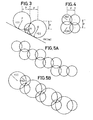
- FIG.lA shows a part of a picture which is to be printed
- picture elements (dots) A through X which constitute a part of the picture are represented by square blocks for convenience' sake.
- FIG.1B shows an example of the dots which are to be printed in correspondence with FIG.1A
- the dots which are to be printed are represented by "1" and the dots which are not to be printed are represented by "0".
- the printing areas of the dots which are to be printed are constant, an unwanted gap may be formed between adjacent dots, and moreover, an oblique line in the picture will be printed as an unnaturally-looking staircase line. As a result, the printed picture will look unnatural.
- the printing area of each dot is variably set depending on a dot pattern which is formed by each dot and the dots surrounding each dot.
- the present inventor obtained by simulations performed on a simulator how the area of a center dot should be set depending on the dot pattern which is formed by the center and the surrounding dots.
- each dot has one of four possible printing areas which are a large area, a medium area, a small area, and zero
- FIG.2B it was found that an unwanted gap will not be formed between adjacent dots and a naturally-looking printed picture is obtainable when the center dot has the medium printing area.
- the pitch (interval) between centers of the dots is represented by p, the following equation (1) must stand in order for the dot F to make contact with the dot O.
- a medium radius r (m) for obtaining the medium printing area should be selected to such a value that a gap is not formed between the adjacent dots even when three adjacent dots all have the small radius r (s) as shown in FIG.4, and in this case, the following equation (3) should stand.
- a ratio of the dot radii r (l) , r (m) , and r (s) should be selected to r (l) :r (m ):r (s) 11.2:7.5:6.7.
- the printing area of each dot is set to the optimum printing area depending on the printing areas of the dots surrounding each dot.
- the dots shown in FIG.1B are printed with the printing areas shown in FIG.1C, for example, where "3", “2", “1”, and “0” in FIG.1C respectively represent the large, medium, small, and zero printing areas (that is, the dot radii are r (l) , r (m) , r (s) , and zero).
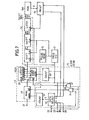
- a composite video signal is applied to an input terminal 10 and is supplied to a synchronizing signal separating circuit 11.
- the synchronizing signal separating circuit 11 has a known circuit construction.
- the synchronizing signal separating circuit 11 separates horizontal and vertical synchronizing signals from the composite video signal and also generates a predetermined clock signal based on the separated synchronizing signals.
- An output video signal of the synchronizing signal separating circuit 11 is supplied to an analog-to-digital (A/D) converting circuit 12 and is converted into a digital video signal which describes the picture information in a binary format.
- the output digital video signal of the A/D converting circuit 12 is supplied to .
- a picture information memory 13 stores the picture information corresponding to one picture, for example.
- the horizontal and vertical synchronizing signals and the clock signal from the synchronizing signal separating circuit 11 are supplied to an address generating circuit 14.
- a pulse generating circuit 15 generates a first clock pulse and supplies the first clock pulse to a shift register circuit 16 and a frequency divider 17.
- the frequency divider 17 produces a second clock pulse by frequency-dividing the first clock pulse, and this second clock pulse is supplied to the shift register circuit 16, the address generating circuit 14, and a printer 19 which will be described later on in the specification.
- a page synchronizing signal and a line synchronizing signal from the printer 19 are also supplied to the address generating circuit 14.
- the address generating circuit 14 successively generates write-in addresses for writing into the memory 13 the picture information corresponding to one picture, for example.
- the address generating circuit 15 successively generates read-out addresses for reading out from the memory 13 a datum of one dot and data of the dots surrounding the one dot.
- the data of the dots A, B, C, E, F, G, I, J, and K shown in FIG.lA are successively read out from the memory 13, for example, and are supplied to the shift register circuit 16.
- the shift register circuit 16 supplies the data from the memory 13 to a memory 18 as a parallel datum constituted by the data of the one and the surrounding dots.
- the memory 18 pre-stores therein in the form of a table the optimum printing areas of the dots which are dependent on the dot patterns and are obtained by the simulation and the calculation described before.
- a printing datum in the table within the memory 18 is read out from the memory 18 according to the output parallel datum of the shift register circuit 16 describing the dot pattern, and the read out printing datum is supplied to the printer 19.
- the printer 19 prints the dot with the printing area described by the printing datum read out from the memory 18, with a timing determined by the output second clock pulse of the frequency divider 17.
- a known printer may be used for the printer 19.
- the printer 19 needs to have such a construction that the printing area of the dot can be controlled, that is, the printing density of the dot can be controlled.
- a themal printer disclosed in a United States Patent No.4,536,771 may be used for the printer 19.
- the printer 19 is not limited to the thermal printer, and other types of printers may be used.
- FIG.7 shows a concrete embodiment of an essential part of the block system shown in FIG.6.
- the memory 13 comprises random access memories (RAMs) 27 and 29 and a latch circuit 28.
- the address generating circuit 14 comprises counters 31 and 33, a data selector 32, and NAND circuits 34 and 35.
- the shift register circuit 16 comprises shift registers 37 and 38 and a latch circuit 39.
- a read only memory (ROM) 18a is used for the memory 18.
- a 1-bit digital dot datum from the A/D converter 12 is applied in series to an input terminal 21.
- a read/write signal which indicates whether the dot datum is to be read out or written is applied to an input terminal 22.
- the clock signal and the horizontal and and vertical synchronizing signals from the synchronizing signal separating circuit 11 are respectively applied to input terminals 23 through 25.
- the data selector 32 When writing in the dot datum, the data selector 32 selectively supplies to the counter 31 the signals from the input terminals 23 through 25 responsive to the read/write signal.
- An inverted signal of the read/write signal and the clock signal from the input terminal 23 are supplied to the NAND circuit 34, and an output signal of the NAND circuit 34 is supplied to a write enable terminal WE of the RAM 27.
- the counter 31 supplies to an address terminal ADDR of the RAM 27 an address signal which designates the write-in address, and the dot datum from the input terminal 21 is written into the designated write-in address within the RAM 27 in synchronism with the clock signal. In this manner, the serial dot data from the input terminal 21 corresponding to one picture, for example, are stored in the RAM 27.
- the data selector 32 selectively supplies to the counter 31 the second clock pulse from the frequency divider 17 and the page and line synchronizing signals from the printer 19 responsive to the read/write signal.
- the frequency divider 17 frequency-divides the first clock pulse from the pulse generating circuit 15 by 1/3 and produces the second clock pulse.
- the counter 31 supplies to the address terminal ADDR of the RAM 27 an address signal which is in synchronism with the second clock pulse and designates the read-out address, and the dot datum read out from the designated read-out address within the RAM 27 is supplied to a first bit input terminal Dl of the latch circuit 28.
- the second clock pulse is supplied to a clock terminal CLK of the latch circuit 28, and a datum from a first bit output terminal Ql of the latch circuit 28 is supplied to a first bit input terminal 11 of the RAM 29 and the shift register 37.
- the counter 33 is supplied with the second clock pulse and the line synchronizing signal, and supplies to an address terminal ADDR of the RAM 29 an address signal which designates an address within the RAM 29.
- the NAND circuit 35 is supplied with the read/write signal and the second clock pulse, and an output signal of the NAND circuit 35 is supplied to a write enable terminal WE of the RAM 29.
- the datum from the first bit output terminal Ql of the latch circuit 28 is written into the the RAM 29 in synchronism with the output signal of the NAND circuit 35 at the address which is designated by the output address signal of the counter 33.
- a read out datum from a first bit output terminal 01 of the RAM 29 is supplied to a second bit input terminal D2 of the latch circuit 28, and the datum from a second bit output terminal Q2 of the latch circuit 28 is supplied to a second bit input terminal I2 of the RAM 29 and the shift register 37.
- the datum from the second bit output terminal 02 of the RAM 29 is supplied to a third bit input terminal D3, and the datum from a third bit output terminal Q3 of the latch circuit 28 is supplied to the shift register 37.
- the data obtained from the first bit output terminal Ql of the latch circuit 28 is the datum d of the dot K shown in FIG.1A
- the data obtained from the second and third bit output terminals Q2 and Q3 of the latch circuit 28 are the data d J and d I of the dots J and I, respectively.
- the shift register 37 is supplied with the second clock pulse to a load terminal LD thereof and is supplied with the first clock pulse to a clock terminal CLK thereof.
- the shift register 37 converts the 3-bit parallel datum from the latch circuit 28 into 1-bit serial data and supplies the 1-bit serial data to the shift register 38.
- the shift register 38 is supplied with the first clock pulse to a clock terminal CLK thereof, and hence produces a 9-bit parallel datum related to one dot and the eight surrounding dots.
- the 9-bit parallel datum is made up of the data d through d C , d E through d G , and d I through d K of the dots A through C, E through G, and I through K shown in FIG.LA.
- the data of the center dot F and the and the eight surrounding dots A through C, E, G, and I through K are simultaneously obtained from the 9-bit parallel datum.
- the 9-bit parallel datum is supplied to the ROM 18a through the latch circuit 39 which is supplied with the second clock pulse to a clock terminal CLK thereof.
- the ROM 18a pre-stores therein in the form of a table the optimum printing areas of the dots which are dependent on the dot patterns and are obtained by the simulation and the calculation described before.
- the table contains the optimum printing area of the center dot in the dot pattern for all of the dot patterns.
- FIG.8 An embodiment of the contents of a ROM table (the table pre-stored in the ROM 18a) for the present embodiment is shown in FIG.8. In FIG.8, access is made to the ROM table by designating a table address described by a 1 through a 9 .
- the table address is designated by the data d A through d C , d E through d G , and d I through d K of the dots A through C, E through G, and I through K. That is, the table address (a 1 , a 2 , a3, a 4 , a 5 , a 6 , a 7 , a 8 , a 9 ) in this case is equal to the parallel dot datum (dA, d B , d C , d E , d F , d G , d I , d J , d K ).
- the table address (d E , d F , d G , d I , d J , d K , d M , d N , d 0 ) in this case is equal to (0, 1, 0, 0, 1, 1, 0, 0, 1) in the case of the dot data shown in FIG.1B, and an optimum printing area "1" is read out from the ROM table for the dot J, where "1" indicates the small printing area described before.
- the table address in this case is equal to (0, 1, 1, 0, 0, 1, 0, 0, 1), and an optimum printing area "0" is read out from the ROM table for the dot N, where "0" indicates the zero printing area.
- the table address is equal to (0, 1, 0, 0, 1, 1, 0, 1, 1), and an optimum printing area "2" is read out from the ROM table, where "2" indicates the medium printing area described before.
- the printing area of one dot is determined by the 3 x 3 dot pattern which is formed by the one dot and the eight surrounding dots.
- the printing area of one dot may be determined by an m x n dot pattern such as 3 x 5 and 5 x 5 dot patterns, where m and n are odd numbers.
- more than four kinds of printing areas may be used for printing the dots. In this case, it is possible to further improve the smoothness with which the oblique lines in the picture are printed.
- the picture information processing system of the present invention in the case where an output device having the same resolution as that of an output device employed in a conventional picture information processing system is employed, it is possible to obtain a picture which looks extremely smooth and natural compared to the picture obtained in the conventional case.
- the picture elements constituting one picture are respectively printed by use of one dot.
- the present invention is also applicable to a system which divides one picture element into a matrix of a plurality of dots and describes one picture element by the dot matrix.
- the picture elements shown in FIG.lA are respectively divided into the 3 x 3 dot matrix and printed as shown in part in FIG.9.
- the picture element J is described and printed by dots Jl through J9.
- each dot can be printed with the optimum printing area.
- a printer having a relatively high resolution is required, but on the other hand, it is possible to obtain a printed picture in which the oblique lines are extremely well smoothened.
Landscapes
- Engineering & Computer Science (AREA)
- Multimedia (AREA)
- Signal Processing (AREA)
- Dot-Matrix Printers And Others (AREA)
- Editing Of Facsimile Originals (AREA)
- Television Signal Processing For Recording (AREA)
- Image Processing (AREA)
- Facsimile Image Signal Circuits (AREA)
Applications Claiming Priority (2)
| Application Number | Priority Date | Filing Date | Title |
|---|---|---|---|
| JP60010493A JPS61170185A (ja) | 1985-01-23 | 1985-01-23 | 画素情報処理方式 |
| JP10493/85 | 1985-01-23 |
Publications (3)
| Publication Number | Publication Date |
|---|---|
| EP0189325A2 true EP0189325A2 (de) | 1986-07-30 |
| EP0189325A3 EP0189325A3 (en) | 1988-09-14 |
| EP0189325B1 EP0189325B1 (de) | 1991-12-27 |
Family
ID=11751707
Family Applications (1)
| Application Number | Title | Priority Date | Filing Date |
|---|---|---|---|
| EP86300462A Expired EP0189325B1 (de) | 1985-01-23 | 1986-01-23 | Bildinformationsverarbeitungssystem |
Country Status (4)
| Country | Link |
|---|---|
| US (1) | US4677493A (de) |
| EP (1) | EP0189325B1 (de) |
| JP (1) | JPS61170185A (de) |
| DE (2) | DE3683060D1 (de) |
Cited By (4)
| Publication number | Priority date | Publication date | Assignee | Title |
|---|---|---|---|---|
| WO1990006653A1 (en) * | 1988-12-02 | 1990-06-14 | Image Processing Technologies, Inc. | Method and apparatus for digitizing an image |
| EP0356038A3 (de) * | 1988-08-16 | 1990-12-05 | Hewlett-Packard Company | Stückweise Druckbildvergrösserung für Punktmatrixdrucker |
| DE10026995C2 (de) * | 1999-06-04 | 2003-10-23 | Ricoh Kk | Bilderzeugungsverfahren und -vorrichtung |
| DE10126625B4 (de) * | 2000-08-23 | 2006-06-14 | Hewlett-Packard Development Co., L.P., Houston | Bilddruckvorrichtung, Verfahren zum Drucken eines Bildes und Computerprogramm |
Families Citing this family (12)
| Publication number | Priority date | Publication date | Assignee | Title |
|---|---|---|---|---|
| JPS6367073A (ja) * | 1986-09-08 | 1988-03-25 | Canon Inc | レ−ザ光変調方式 |
| JP2589295B2 (ja) * | 1986-11-14 | 1997-03-12 | キヤノン株式会社 | 画像形成装置 |
| US6529637B1 (en) | 1989-05-22 | 2003-03-04 | Pixel Instruments Corporation | Spatial scan replication circuit |
| US7382929B2 (en) | 1989-05-22 | 2008-06-03 | Pixel Instruments Corporation | Spatial scan replication circuit |
| US5130821A (en) * | 1990-04-16 | 1992-07-14 | Eastman Kodak Company | Method and apparatus for digital halftoning employing density distribution for selection of a threshold template |
| DE4038056C2 (de) * | 1990-11-29 | 1997-05-15 | Hell Ag Linotype | Verfahren zur Generierung und Speicherung von digitalisierten Dichteschwellwerten zur Rasterung einer Halbton-Bildvorlage |
| DE4038057C2 (de) * | 1990-11-29 | 1997-05-15 | Hell Ag Linotype | Verfahren zur Generierung und Speicherung von digitalisierten Dichteschwellwerten zur Rasterung einer Halbtonbildvorlage |
| US5438437A (en) * | 1991-10-17 | 1995-08-01 | Konica Corporation | Image forming apparatus with exposure, size, and position correction for pixels |
| JP3119150B2 (ja) * | 1995-02-02 | 2000-12-18 | 富士ゼロックス株式会社 | 画像処理装置および画像処理方法 |
| US7492480B2 (en) * | 2001-08-27 | 2009-02-17 | Phototype Engraving Company | System for halftone screen production |
| US20030058458A1 (en) * | 2001-09-24 | 2003-03-27 | Ripit Computer Corporation | Image-processing for output on a proofing device |
| JP3982817B2 (ja) * | 2003-03-07 | 2007-09-26 | 株式会社東芝 | 画像処理装置および画像処理方法 |
Family Cites Families (9)
| Publication number | Priority date | Publication date | Assignee | Title |
|---|---|---|---|---|
| DE1137477B (de) * | 1960-11-12 | 1962-10-04 | Standard Elektrik Lorenz Ag | Verfahren zur UEbertragung von auf einen Aufzeichnungstraeger in Bild oder Schrift aufgezeichneten Informationen |
| DE1772367C3 (de) * | 1968-05-04 | 1974-10-31 | Dr.-Ing. Rudolf Hell Gmbh, 2300 Kiel | Verfahren zur gerasterten Reproduktion von Halbtonbildern |
| US3977007A (en) * | 1975-06-02 | 1976-08-24 | Teletype Corporation | Gray tone generation |
| US4196451A (en) * | 1976-05-21 | 1980-04-01 | Xerox Corporation | Electronic halftone generator |
| JPS6027464B2 (ja) * | 1976-09-28 | 1985-06-28 | 日本電気株式会社 | 高画素密度変換装置 |
| US4122496A (en) * | 1977-02-23 | 1978-10-24 | International Business Machines Corporation | Apparatus and method for digital halftone reproduction |
| US4212009A (en) * | 1977-11-16 | 1980-07-08 | Hewlett-Packard Company | Smoothing a raster display |
| US4430748A (en) * | 1981-09-21 | 1984-02-07 | Xerox Corporation | Image thresholding system |
| JPS60258584A (ja) * | 1984-06-05 | 1985-12-20 | 株式会社 写研 | 文字の表現方法及び装置 |
-
1985
- 1985-01-23 JP JP60010493A patent/JPS61170185A/ja active Pending
-
1986
- 1986-01-21 US US06/821,030 patent/US4677493A/en not_active Expired - Fee Related
- 1986-01-23 DE DE8686300462T patent/DE3683060D1/de not_active Expired - Fee Related
- 1986-01-23 EP EP86300462A patent/EP0189325B1/de not_active Expired
- 1986-01-23 DE DE198686300462T patent/DE189325T1/de active Pending
Cited By (5)
| Publication number | Priority date | Publication date | Assignee | Title |
|---|---|---|---|---|
| EP0356038A3 (de) * | 1988-08-16 | 1990-12-05 | Hewlett-Packard Company | Stückweise Druckbildvergrösserung für Punktmatrixdrucker |
| EP0710565A3 (de) * | 1988-08-16 | 1996-05-15 | Hewlett-Packard Company | Stückweise Druckbildverbesserung für Punktmatrixdrucker |
| WO1990006653A1 (en) * | 1988-12-02 | 1990-06-14 | Image Processing Technologies, Inc. | Method and apparatus for digitizing an image |
| DE10026995C2 (de) * | 1999-06-04 | 2003-10-23 | Ricoh Kk | Bilderzeugungsverfahren und -vorrichtung |
| DE10126625B4 (de) * | 2000-08-23 | 2006-06-14 | Hewlett-Packard Development Co., L.P., Houston | Bilddruckvorrichtung, Verfahren zum Drucken eines Bildes und Computerprogramm |
Also Published As
| Publication number | Publication date |
|---|---|
| EP0189325B1 (de) | 1991-12-27 |
| US4677493A (en) | 1987-06-30 |
| JPS61170185A (ja) | 1986-07-31 |
| EP0189325A3 (en) | 1988-09-14 |
| DE3683060D1 (de) | 1992-02-06 |
| DE189325T1 (de) | 1986-11-06 |
Similar Documents
| Publication | Publication Date | Title |
|---|---|---|
| US4677493A (en) | Picture information processing system | |
| US4149194A (en) | Variable angle electronic halftone screening | |
| US4555191A (en) | Method of reducing character font | |
| US4686580A (en) | Method and apparatus for changing image size | |
| CA1114747A (en) | Electronic halftone screening with halftone cells approximating a parallelogram | |
| US3778810A (en) | Display device | |
| US4447882A (en) | Method and apparatus for reducing graphic patterns | |
| CA1224291A (en) | Raster scan display system | |
| US4533942A (en) | Method and apparatus for reproducing an image which has a coarser resolution than utilized in scanning of the image | |
| GB1522098A (en) | Digital raster display system | |
| US6389161B1 (en) | Method of interpolation in an n-dimensional color space | |
| EP0139095A2 (de) | Bildauswahl in einem Rasteranzeigesystem | |
| US4953104A (en) | Page buffer for an electronic gray-scale color printer | |
| US4563677A (en) | Digital character display | |
| US4326201A (en) | Apparatus for displaying characters | |
| US5239391A (en) | Apparatus for generating halftone dots from dot envelope parameters | |
| US5233441A (en) | Method for representing halftone dots with dot envelope parameters | |
| US4627749A (en) | Character generator system for dot matrix printers | |
| EP0091124B1 (de) | Videosignalerzeugerkreis | |
| US5337409A (en) | Parallel/serial data conversion system | |
| US4903147A (en) | Method and apparatus for processing an image | |
| EP0284326B1 (de) | Generator von Musteranzeigesignalen und Anzeigegerät mit Verwendung dieser Signale | |
| US5553204A (en) | Image output apparatus for gradation image data | |
| US5446558A (en) | Apparatus and associated method for representing elliptical halftone dots | |
| US5347597A (en) | Image scaling for thermal printers and the like |
Legal Events
| Date | Code | Title | Description |
|---|---|---|---|
| PUAI | Public reference made under article 153(3) epc to a published international application that has entered the european phase |
Free format text: ORIGINAL CODE: 0009012 |
|
| AK | Designated contracting states |
Kind code of ref document: A2 Designated state(s): DE FR GB |
|
| EL | Fr: translation of claims filed | ||
| DET | De: translation of patent claims | ||
| 17P | Request for examination filed |
Effective date: 19860912 |
|
| PUAL | Search report despatched |
Free format text: ORIGINAL CODE: 0009013 |
|
| AK | Designated contracting states |
Kind code of ref document: A3 Designated state(s): DE FR GB |
|
| 17Q | First examination report despatched |
Effective date: 19901120 |
|
| GRAA | (expected) grant |
Free format text: ORIGINAL CODE: 0009210 |
|
| AK | Designated contracting states |
Kind code of ref document: B1 Designated state(s): DE FR GB |
|
| REF | Corresponds to: |
Ref document number: 3683060 Country of ref document: DE Date of ref document: 19920206 |
|
| ET | Fr: translation filed | ||
| PLBE | No opposition filed within time limit |
Free format text: ORIGINAL CODE: 0009261 |
|
| STAA | Information on the status of an ep patent application or granted ep patent |
Free format text: STATUS: NO OPPOSITION FILED WITHIN TIME LIMIT |
|
| 26N | No opposition filed | ||
| PGFP | Annual fee paid to national office [announced via postgrant information from national office to epo] |
Ref country code: FR Payment date: 19940111 Year of fee payment: 9 |
|
| PGFP | Annual fee paid to national office [announced via postgrant information from national office to epo] |
Ref country code: GB Payment date: 19940113 Year of fee payment: 9 |
|
| PGFP | Annual fee paid to national office [announced via postgrant information from national office to epo] |
Ref country code: DE Payment date: 19940121 Year of fee payment: 9 |
|
| PG25 | Lapsed in a contracting state [announced via postgrant information from national office to epo] |
Ref country code: GB Effective date: 19950123 |
|
| GBPC | Gb: european patent ceased through non-payment of renewal fee |
Effective date: 19950123 |
|
| PG25 | Lapsed in a contracting state [announced via postgrant information from national office to epo] |
Ref country code: FR Effective date: 19950929 |
|
| PG25 | Lapsed in a contracting state [announced via postgrant information from national office to epo] |
Ref country code: DE Effective date: 19951003 |
|
| REG | Reference to a national code |
Ref country code: FR Ref legal event code: ST |