EP0187918B1 - Filtre à ondes acoustiques de surface - Google Patents
Filtre à ondes acoustiques de surface Download PDFInfo
- Publication number
- EP0187918B1 EP0187918B1 EP85114644A EP85114644A EP0187918B1 EP 0187918 B1 EP0187918 B1 EP 0187918B1 EP 85114644 A EP85114644 A EP 85114644A EP 85114644 A EP85114644 A EP 85114644A EP 0187918 B1 EP0187918 B1 EP 0187918B1
- Authority
- EP
- European Patent Office
- Prior art keywords
- substrate
- interdigital transducer
- damping material
- wave filter
- bus bars
- Prior art date
- Legal status (The legal status is an assumption and is not a legal conclusion. Google has not performed a legal analysis and makes no representation as to the accuracy of the status listed.)
- Expired - Lifetime
Links
Images

Classifications
-
- H—ELECTRICITY
- H03—ELECTRONIC CIRCUITRY
- H03H—IMPEDANCE NETWORKS, e.g. RESONANT CIRCUITS; RESONATORS
- H03H9/00—Networks comprising electromechanical or electro-acoustic devices; Electromechanical resonators
- H03H9/02—Details
- H03H9/02535—Details of surface acoustic wave devices
- H03H9/02614—Treatment of substrates, e.g. curved, spherical, cylindrical substrates ensuring closed round-about circuits for the acoustical waves
- H03H9/02622—Treatment of substrates, e.g. curved, spherical, cylindrical substrates ensuring closed round-about circuits for the acoustical waves of the surface, including back surface
-
- H—ELECTRICITY
- H03—ELECTRONIC CIRCUITRY
- H03H—IMPEDANCE NETWORKS, e.g. RESONANT CIRCUITS; RESONATORS
- H03H9/00—Networks comprising electromechanical or electro-acoustic devices; Electromechanical resonators
- H03H9/02—Details
- H03H9/02535—Details of surface acoustic wave devices
- H03H9/02614—Treatment of substrates, e.g. curved, spherical, cylindrical substrates ensuring closed round-about circuits for the acoustical waves
- H03H9/02629—Treatment of substrates, e.g. curved, spherical, cylindrical substrates ensuring closed round-about circuits for the acoustical waves of the edges
Definitions
- the invention relates to a surface acoustic wave filter according to the preamble of patent claim 1.
- Surface wave filters are known for example from the data book “Surface Wave Filters LIOB", edition 1983/84, published by Siemens. They represent integrated, passive components with bandpass filter characteristics, the function of which is based on the interference of surface mechanical waves that propagate along the surface of a piezoelectric material. Its structure is characterized by a single-crystal, piezoelectric substrate, in particular made of lithium niobate, onto which a metal layer, in particular aluminum layer, is applied, for example vapor-deposited, from which piezoelectric input and output transducers, so-called interdigital transducers, have been worked out by means of photoetching technology.
- Electrodes consist of several metallized comb-like electrodes, ie electrodes with busbars and fingers oriented perpendicular to these, which overlap each other with fingers of the electrodes of different polarity in the active regions of the transducers.
- the substrate itself is glued to a metal support. The contacting of the input and output converters with the connections leading to the outside takes place via bond wires.
- a signal input into the input transducer is converted into a mechanical surface acoustic wave which runs on or in the surface of the substrate for the output conversion, which finally converts the surface acoustic wave into an electrical signal.
- the conventional converters already mentioned above have interdigital structures with time-of-flight effects, which can be provided with a structure for shielding. They have strongly frequency-dependent properties, so that a filter effect for electrical signals can be achieved due to the structure of the structures.
- the waves excited in the overlap areas of the electrodes of the interdigital transducers not only propagate in the desired direction of propagation but also, in the direction of the substrate or chip edges, due to diffraction phenomena and the source distribution determined by the interdigital structures.
- the waves running towards the short substrate edges are damped in the usual damping technique using a wide variety of materials, in particular photoresist and / or screen printing varnish, which are applied to the corresponding substrate surface using the photoresist or screen printing method.
- the photoresist process has proven to be particularly suitable, since it is the best way to produce the fine structures of the damping materials to be realized.
- the present invention has for its object to provide a surface acoustic wave filter, which if necessary if, in addition to the known damping already mentioned, the waves are damped or largely suppressed, which run towards the longitudinal edges of the substrate and are reflected at the transition from the transducer structure, in particular at the transition from the busbars of the electrodes to the free substrate surface and at the longitudinal edges of the substrate.
- the invention provides for an electrical surface acoustic wave filter according to the preamble of claim 1 that the damping mass is applied in strips parallel to the longitudinal substrate edges to parts of the inactive interdigital transducer region between the longitudinal substrate edges and the active interdigital transducer region, the damping mass being at least the busbars of an interdigital transducer completely and additionally at least partially covering inactive interdigital transducer regions adjacent to it.
- the damping mass in particular photoresist and / or screen printing varnish, can in addition to the busbars cover the entire area between these busbars and the adjacent longitudinal substrate edges and the area between these busbars and the active interdigital transducer area determined by the electrode fingers with the greatest overlap.
- the overlap-free, inactive interdigital transducer area is preferably chosen so large by choosing a suitable electrode finger length that sufficient area is available for the application of the damping mass.
- interdigital transducers IW 1 and IW 2 have a plate-shaped substrate 1 made of single-crystal, piezoelectric material, namely lithium niobate.
- substrate 1 made of single-crystal, piezoelectric material, namely lithium niobate.
- One side of the substrate contributes to the excitation and coupling of the surface waves interdigital transducers IW 1 and IW 2.
- Both interdigital transducers consist, for example, of metallic structures vapor-deposited on the substrate, the electrodes of which are comb-shaped and overlap with their electrode fingers 17, 18 in the active interdigital transducer regions.
- the electrode fingers of the interdigital transducers are each connected via busbars 3, 22; 2 or 15, 16 and contact surfaces 7; 6 or 19; 20, 21 turned on.
- each damping mass 10 or 11 covers an inactive interdigital transducer region a, a; ie an area in which the electrode fingers of different polarity, indicated only by their ends, do not overlap, and additionally the busbars 3 and 2.
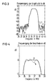
- FIGS. 3.4 show the filter pass-through curves for a surface acoustic wave filter according to FIG. ie the frequency response of the amplitude plotted against the frequency, expressed in dB. With “a” is the pass curve, which is used when damping the filter along the short and long edge of the substrate 8 or 4, 5 receives; whereas the curve "b” only shows the values that are obtained along the short substrate edge 8 with exclusive damping.
Claims (4)
- Filtre électrique à ondes de surface comportant un substrat en forme de plaquette constitué par un matériau piézoélectrique monocristallin, notamment du niobate de lithium et dont une face porte des transducteurs interdigités utilisés pour l'excitation et le couplage des ondes de surface et constitués par des électrodes en forme de peignes qui s'interpénètrent et comportent des barres collectrice métalliques respectives et des doigts, que contactent ces barres collectrices et qui se chevauchent dans les régions actives des transducteurs interdigités, qui excitent ou reçoivent les ondes de surface, et comportant une masse plastique d'amortissement, une masse élastique d'amortissement ou une combinaison de ces masses d'amortissement, qui sert à supprimer des réflexions d'ondes parasites, qui apparaissent dans le substrat, caractérisé par le fait que la masse d'amortissement est déposée sous la forme de bandes parallèles aux grands côtés du substrat, sur des parties de la région inactive des transducteurs interdigités entre les grands côtés du substrat et la région active des transducteurs interdigités, la masse d'amortissement recouvrant complètement au moins les barres collectrices d'un transducteur interdigité et en outre au moins partiellement des régions inactives des transducteurs interdigités, qui jouxtent ces barres.
- Filtre électrique d'ondes de surface suivant la revendication 1, caractérisé par le fait que la masse d'amortissement recouvre, outre les barres collectrices, l'ensemble de la région située entre ces barres collectrices et les grands côtés du substrat, voisins de ces barres, et recouvre la région située entre ces barres collectrices et la région active des transducteurs interdigités, qui est déterminée par le chevauchement maximum par les doigts des électrodes.
- Filtre électrique de surface suivant la revendication 1, caractérisé par le fait que grâce au choix d'une longueur appropriée des doigts des électrodes, la région inactive des transducteurs interdigités qui ne comporte aucun chevauchement, est suffisamment étendue pour qu'une surface suffisante soit disponible pour le dépôt de la masse d'amortissement.
- Filtre électrique d'ondes de surface suivant la revendication 1, caractérisé par le fait que la masse d'amortissement est une laque photosensible et/ou une laque de sérigraphie.
Applications Claiming Priority (2)
| Application Number | Priority Date | Filing Date | Title |
|---|---|---|---|
| DE3446022 | 1984-12-17 | ||
| DE3446022 | 1984-12-17 |
Publications (2)
| Publication Number | Publication Date |
|---|---|
| EP0187918A1 EP0187918A1 (fr) | 1986-07-23 |
| EP0187918B1 true EP0187918B1 (fr) | 1991-07-24 |
Family
ID=6253012
Family Applications (1)
| Application Number | Title | Priority Date | Filing Date |
|---|---|---|---|
| EP85114644A Expired - Lifetime EP0187918B1 (fr) | 1984-12-17 | 1985-11-18 | Filtre à ondes acoustiques de surface |
Country Status (5)
| Country | Link |
|---|---|
| US (1) | US4672338A (fr) |
| EP (1) | EP0187918B1 (fr) |
| JP (1) | JPS61245613A (fr) |
| DE (1) | DE3583602D1 (fr) |
| ES (1) | ES8702093A1 (fr) |
Families Citing this family (6)
| Publication number | Priority date | Publication date | Assignee | Title |
|---|---|---|---|---|
| JPS63266913A (ja) * | 1987-04-22 | 1988-11-04 | Showa Electric Wire & Cable Co Ltd | 弾性表面波装置 |
| JPS63266912A (ja) * | 1987-04-22 | 1988-11-04 | Showa Electric Wire & Cable Co Ltd | 弾性表面波装置 |
| NL9220007A (nl) * | 1991-10-17 | 1993-10-01 | Rif O Z Mikroelektroniki | Met akoestische oppervlaktegolven werkend banddoorlaatfilter |
| RU2121213C1 (ru) * | 1991-10-17 | 1998-10-27 | Акционерное общество открытого типа "РИФ" | Полосовой фильтр на поверхностных акустических волнах (пав) |
| JP3154402B2 (ja) * | 1997-11-12 | 2001-04-09 | 日本電気株式会社 | Sawフィルタ |
| GB9911878D0 (en) * | 1999-05-22 | 1999-07-21 | Marconi Electronic Syst Ltd | Identification tag |
Family Cites Families (9)
| Publication number | Priority date | Publication date | Assignee | Title |
|---|---|---|---|---|
| JPS5333557A (en) * | 1976-08-24 | 1978-03-29 | Toshiba Corp | Elastic surface wave element |
| US4322651A (en) * | 1977-05-09 | 1982-03-30 | Murata Manufacturing Co., Ltd. | Acoustic surface wave device |
| EP0097642A1 (fr) * | 1981-12-14 | 1984-01-11 | Gte Products Corporation | Cire acoustique sur un dispositif a ondes de surface |
| JPS58131809A (ja) * | 1982-01-30 | 1983-08-05 | Toshiba Corp | 弾性表面波素子 |
| JPS598419A (ja) * | 1982-07-07 | 1984-01-17 | Hitachi Ltd | 弾性表面波装置 |
| US4472694A (en) * | 1982-09-07 | 1984-09-18 | Gte Laboratories Incorporated | Acoustic surface wave device |
| GB2127249A (en) * | 1982-09-20 | 1984-04-04 | Philips Electronic Associated | Acoustic surface wave device |
| DE3234955A1 (de) * | 1982-09-21 | 1984-03-22 | Siemens AG, 1000 Berlin und 8000 München | Oberflaechenwellenfilter, sowie verfahren zur herstellung des oberflaechenwellenfilters |
| DE3235236A1 (de) * | 1982-09-23 | 1984-03-29 | Siemens AG, 1000 Berlin und 8000 München | Oberflaechenwellenfilter, sowie verfahren zur herstellung einer bedaempfungsschicht fuer oberflaechenwellenfilter |
-
1985
- 1985-11-18 DE DE8585114644T patent/DE3583602D1/de not_active Expired - Fee Related
- 1985-11-18 EP EP85114644A patent/EP0187918B1/fr not_active Expired - Lifetime
- 1985-12-05 US US06/806,248 patent/US4672338A/en not_active Expired - Lifetime
- 1985-12-12 JP JP60280149A patent/JPS61245613A/ja active Pending
- 1985-12-17 ES ES550030A patent/ES8702093A1/es not_active Expired
Also Published As
| Publication number | Publication date |
|---|---|
| ES8702093A1 (es) | 1986-12-01 |
| DE3583602D1 (de) | 1991-08-29 |
| EP0187918A1 (fr) | 1986-07-23 |
| ES550030A0 (es) | 1986-12-01 |
| JPS61245613A (ja) | 1986-10-31 |
| US4672338A (en) | 1987-06-09 |
Similar Documents
| Publication | Publication Date | Title |
|---|---|---|
| DE19849782B4 (de) | Oberflächenwellenanordnung mit zumindest zwei Oberflächenwellen-Strukturen | |
| EP0988697B1 (fr) | Filtre a ondes de surface bimode | |
| DE112015001771T5 (de) | Filtervorrichtung für elastische Wellen | |
| EP0187918B1 (fr) | Filtre à ondes acoustiques de surface | |
| DE19838573B4 (de) | Oberflächenwellenfilter | |
| DE112013002520T5 (de) | Bauelement für elastische Wellen | |
| DE2133634A1 (de) | Elektrisches filter nach dem oberflaechenwellenprinzip | |
| WO1991009465A1 (fr) | Filtre-reflecteur d'ondes superficielles | |
| DE102018118384A1 (de) | Hochfrequenzfilter | |
| DE2826891C3 (de) | Elastizitätsoberflächenwellen-Bauelement | |
| DE2512671A1 (de) | Mit akustischen oberflaechenwellen in einem ausgewaehlten frequenzbereich arbeitendes geraet | |
| WO2012076517A1 (fr) | Convertisseur electro-acoustique a pertes reduites grace a une emission transversale, et de meilleure perfomance due a la suppression de modes transversaux | |
| DE2820046C2 (de) | Akustisches Oberflächenwellen- Bauelement | |
| DE3015903A1 (de) | Wandler o.dgl. element fuer akustische oberflaechenwellen | |
| EP0367864B1 (fr) | Dispositif à ondes acoustiques de surface à bande passante variable | |
| DE3811989A1 (de) | Oberflaechenwellenconvolver | |
| DE4132309A1 (de) | Stoneleywellen-bauteil mit nicht-reflektierenden interdigitalwandlern | |
| EP0154698A2 (fr) | Filtre électrique à ondes acoustiques de surface | |
| DE102012110504A1 (de) | Elektroakustisches Filter mit Tiefpasscharakteristik | |
| EP0106189A2 (fr) | Filtre à ondes acoustiques de surface et méthode de fabrication d'un tel filtre | |
| EP0188263A1 (fr) | Filtre à ondes acoustiques de surface | |
| DE69730189T2 (de) | Unidirektionales Filter mit akustischen Oberflächenwellen | |
| DE3018080C2 (de) | Akustisches Oberflächenwellenfilter | |
| DE19724255C2 (de) | Transversalmodenresonatorfilter | |
| DE2235233B2 (de) | Filter oder verzoegerungsleitung nach dem oberflaechenwellenprinzip |
Legal Events
| Date | Code | Title | Description |
|---|---|---|---|
| PUAI | Public reference made under article 153(3) epc to a published international application that has entered the european phase |
Free format text: ORIGINAL CODE: 0009012 |
|
| 17P | Request for examination filed |
Effective date: 19851126 |
|
| AK | Designated contracting states |
Kind code of ref document: A1 Designated state(s): BE DE FR GB IT |
|
| 17Q | First examination report despatched |
Effective date: 19890323 |
|
| GRAA | (expected) grant |
Free format text: ORIGINAL CODE: 0009210 |
|
| AK | Designated contracting states |
Kind code of ref document: B1 Designated state(s): BE DE FR GB IT |
|
| REF | Corresponds to: |
Ref document number: 3583602 Country of ref document: DE Date of ref document: 19910829 |
|
| ET | Fr: translation filed | ||
| ITF | It: translation for a ep patent filed |
Owner name: STUDIO JAUMANN |
|
| GBT | Gb: translation of ep patent filed (gb section 77(6)(a)/1977) | ||
| PLBE | No opposition filed within time limit |
Free format text: ORIGINAL CODE: 0009261 |
|
| STAA | Information on the status of an ep patent application or granted ep patent |
Free format text: STATUS: NO OPPOSITION FILED WITHIN TIME LIMIT |
|
| 26N | No opposition filed | ||
| PGFP | Annual fee paid to national office [announced via postgrant information from national office to epo] |
Ref country code: BE Payment date: 19921117 Year of fee payment: 8 |
|
| PG25 | Lapsed in a contracting state [announced via postgrant information from national office to epo] |
Ref country code: BE Effective date: 19931130 |
|
| BERE | Be: lapsed |
Owner name: SIEMENS A.G. Effective date: 19931130 |
|
| REG | Reference to a national code |
Ref country code: FR Ref legal event code: TP |
|
| REG | Reference to a national code |
Ref country code: GB Ref legal event code: IF02 |
|
| PGFP | Annual fee paid to national office [announced via postgrant information from national office to epo] |
Ref country code: DE Payment date: 20021202 Year of fee payment: 18 |
|
| PG25 | Lapsed in a contracting state [announced via postgrant information from national office to epo] |
Ref country code: DE Free format text: LAPSE BECAUSE OF NON-PAYMENT OF DUE FEES Effective date: 20040602 |
|
| PGFP | Annual fee paid to national office [announced via postgrant information from national office to epo] |
Ref country code: GB Payment date: 20041110 Year of fee payment: 20 |
|
| PGFP | Annual fee paid to national office [announced via postgrant information from national office to epo] |
Ref country code: FR Payment date: 20041119 Year of fee payment: 20 |
|
| PG25 | Lapsed in a contracting state [announced via postgrant information from national office to epo] |
Ref country code: GB Free format text: LAPSE BECAUSE OF EXPIRATION OF PROTECTION Effective date: 20051117 |
|
| REG | Reference to a national code |
Ref country code: GB Ref legal event code: PE20 |