EP0187918B1 - Electrical surface wave filter - Google Patents
Electrical surface wave filter Download PDFInfo
- Publication number
- EP0187918B1 EP0187918B1 EP85114644A EP85114644A EP0187918B1 EP 0187918 B1 EP0187918 B1 EP 0187918B1 EP 85114644 A EP85114644 A EP 85114644A EP 85114644 A EP85114644 A EP 85114644A EP 0187918 B1 EP0187918 B1 EP 0187918B1
- Authority
- EP
- European Patent Office
- Prior art keywords
- substrate
- interdigital transducer
- damping material
- wave filter
- bus bars
- Prior art date
- Legal status (The legal status is an assumption and is not a legal conclusion. Google has not performed a legal analysis and makes no representation as to the accuracy of the status listed.)
- Expired - Lifetime
Links
Images

Classifications
-
- H—ELECTRICITY
- H03—ELECTRONIC CIRCUITRY
- H03H—IMPEDANCE NETWORKS, e.g. RESONANT CIRCUITS; RESONATORS
- H03H9/00—Networks comprising electromechanical or electro-acoustic devices; Electromechanical resonators
- H03H9/02—Details
- H03H9/02535—Details of surface acoustic wave devices
- H03H9/02614—Treatment of substrates, e.g. curved, spherical, cylindrical substrates ensuring closed round-about circuits for the acoustical waves
- H03H9/02622—Treatment of substrates, e.g. curved, spherical, cylindrical substrates ensuring closed round-about circuits for the acoustical waves of the surface, including back surface
-
- H—ELECTRICITY
- H03—ELECTRONIC CIRCUITRY
- H03H—IMPEDANCE NETWORKS, e.g. RESONANT CIRCUITS; RESONATORS
- H03H9/00—Networks comprising electromechanical or electro-acoustic devices; Electromechanical resonators
- H03H9/02—Details
- H03H9/02535—Details of surface acoustic wave devices
- H03H9/02614—Treatment of substrates, e.g. curved, spherical, cylindrical substrates ensuring closed round-about circuits for the acoustical waves
- H03H9/02629—Treatment of substrates, e.g. curved, spherical, cylindrical substrates ensuring closed round-about circuits for the acoustical waves of the edges
Definitions
- the invention relates to a surface acoustic wave filter according to the preamble of patent claim 1.
- Surface wave filters are known for example from the data book “Surface Wave Filters LIOB", edition 1983/84, published by Siemens. They represent integrated, passive components with bandpass filter characteristics, the function of which is based on the interference of surface mechanical waves that propagate along the surface of a piezoelectric material. Its structure is characterized by a single-crystal, piezoelectric substrate, in particular made of lithium niobate, onto which a metal layer, in particular aluminum layer, is applied, for example vapor-deposited, from which piezoelectric input and output transducers, so-called interdigital transducers, have been worked out by means of photoetching technology.
- Electrodes consist of several metallized comb-like electrodes, ie electrodes with busbars and fingers oriented perpendicular to these, which overlap each other with fingers of the electrodes of different polarity in the active regions of the transducers.
- the substrate itself is glued to a metal support. The contacting of the input and output converters with the connections leading to the outside takes place via bond wires.
- a signal input into the input transducer is converted into a mechanical surface acoustic wave which runs on or in the surface of the substrate for the output conversion, which finally converts the surface acoustic wave into an electrical signal.
- the conventional converters already mentioned above have interdigital structures with time-of-flight effects, which can be provided with a structure for shielding. They have strongly frequency-dependent properties, so that a filter effect for electrical signals can be achieved due to the structure of the structures.
- the waves excited in the overlap areas of the electrodes of the interdigital transducers not only propagate in the desired direction of propagation but also, in the direction of the substrate or chip edges, due to diffraction phenomena and the source distribution determined by the interdigital structures.
- the waves running towards the short substrate edges are damped in the usual damping technique using a wide variety of materials, in particular photoresist and / or screen printing varnish, which are applied to the corresponding substrate surface using the photoresist or screen printing method.
- the photoresist process has proven to be particularly suitable, since it is the best way to produce the fine structures of the damping materials to be realized.
- the present invention has for its object to provide a surface acoustic wave filter, which if necessary if, in addition to the known damping already mentioned, the waves are damped or largely suppressed, which run towards the longitudinal edges of the substrate and are reflected at the transition from the transducer structure, in particular at the transition from the busbars of the electrodes to the free substrate surface and at the longitudinal edges of the substrate.
- the invention provides for an electrical surface acoustic wave filter according to the preamble of claim 1 that the damping mass is applied in strips parallel to the longitudinal substrate edges to parts of the inactive interdigital transducer region between the longitudinal substrate edges and the active interdigital transducer region, the damping mass being at least the busbars of an interdigital transducer completely and additionally at least partially covering inactive interdigital transducer regions adjacent to it.
- the damping mass in particular photoresist and / or screen printing varnish, can in addition to the busbars cover the entire area between these busbars and the adjacent longitudinal substrate edges and the area between these busbars and the active interdigital transducer area determined by the electrode fingers with the greatest overlap.
- the overlap-free, inactive interdigital transducer area is preferably chosen so large by choosing a suitable electrode finger length that sufficient area is available for the application of the damping mass.
- interdigital transducers IW 1 and IW 2 have a plate-shaped substrate 1 made of single-crystal, piezoelectric material, namely lithium niobate.
- substrate 1 made of single-crystal, piezoelectric material, namely lithium niobate.
- One side of the substrate contributes to the excitation and coupling of the surface waves interdigital transducers IW 1 and IW 2.
- Both interdigital transducers consist, for example, of metallic structures vapor-deposited on the substrate, the electrodes of which are comb-shaped and overlap with their electrode fingers 17, 18 in the active interdigital transducer regions.
- the electrode fingers of the interdigital transducers are each connected via busbars 3, 22; 2 or 15, 16 and contact surfaces 7; 6 or 19; 20, 21 turned on.
- each damping mass 10 or 11 covers an inactive interdigital transducer region a, a; ie an area in which the electrode fingers of different polarity, indicated only by their ends, do not overlap, and additionally the busbars 3 and 2.
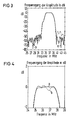
- FIGS. 3.4 show the filter pass-through curves for a surface acoustic wave filter according to FIG. ie the frequency response of the amplitude plotted against the frequency, expressed in dB. With “a” is the pass curve, which is used when damping the filter along the short and long edge of the substrate 8 or 4, 5 receives; whereas the curve "b” only shows the values that are obtained along the short substrate edge 8 with exclusive damping.
Description
Die Erfindung betrifft ein Oberflächenwellenfilter gemäß Oberbegriff des Patentanspruches 1.The invention relates to a surface acoustic wave filter according to the preamble of patent claim 1.
Oberflächenwellenfilter sind z.B. durch das Datenbuch "Oberflächenwellen-Filter LIOB", Ausgabe 1983/84, Herausgeber Siemens, bekannt. Sie stellen integrierte, passive Bauelemente mit Bandfiltercharakteristik dar, deren Funktion auf der Interferenz von mechanischen Oberflächenwellen beruht, die sich längs der Oberfläche eines piezoelektrischen Materials ausbreiten. Ihr Aufbau ist durch ein einkristallines, piezoelektrisches Substrat, insbesondere aus Lithiumniobat, gekennzeichnet, auf das eine Metallschicht, insbesondere Aluminiumschicht, aufgetragen, z.B. aufgedampft ist, aus der mittels Photoätztechnik piezoelektrische Einund Ausgangswandler, sogenannte Interdigitalwandler herausgearbeitet sind. Diese bestehen aus mehreren metallisierten kammartigen Elektroden, d.h. aus Elektroden mit Sammelschienen und senkrecht zu diesen ausgerichteten Fingern, die sich in den aktiven Bereichen der Wandler jeweils mit Fingern der Elektroden unterschiedlicher Polarität überlappen. Das Substrat selbst ist auf einen Metallträger aufgeklebt. Die Kontaktierung der Ein- und Ausgangswandler mit den nach außen führenden Anschlüssen erfolgt dabei über Bond-Drähte.Surface wave filters are known for example from the data book "Surface Wave Filters LIOB", edition 1983/84, published by Siemens. They represent integrated, passive components with bandpass filter characteristics, the function of which is based on the interference of surface mechanical waves that propagate along the surface of a piezoelectric material. Its structure is characterized by a single-crystal, piezoelectric substrate, in particular made of lithium niobate, onto which a metal layer, in particular aluminum layer, is applied, for example vapor-deposited, from which piezoelectric input and output transducers, so-called interdigital transducers, have been worked out by means of photoetching technology. These consist of several metallized comb-like electrodes, ie electrodes with busbars and fingers oriented perpendicular to these, which overlap each other with fingers of the electrodes of different polarity in the active regions of the transducers. The substrate itself is glued to a metal support. The contacting of the input and output converters with the connections leading to the outside takes place via bond wires.
Im Betrieb dieser Oberflächenwellenfilter wird ein in den Eingangswandler eingegebenes Signal in eine mechanische Oberflächenwelle umgewandelt, die auf bzw. in der Oberfläche des Substrats zum Ausgangswandel läuft, der die Oberflächenwelle schließlich in ein elektrisches Signal umwandelt. Die vorstehend bereits erwähnten üblichen Wandler besitzen Interdigitalstrukturen mit Laufzeiteffekten, die mit einer Struktur zur Abschirmung versehen sein können. Sie haben stark frequenzabhängige Eigenschaften, so daß aufgrund der Ausbildung der Strukturen eine Filterwirkung für elektrische Signale erreichbar ist.In the operation of these surface acoustic wave filters, a signal input into the input transducer is converted into a mechanical surface acoustic wave which runs on or in the surface of the substrate for the output conversion, which finally converts the surface acoustic wave into an electrical signal. The conventional converters already mentioned above have interdigital structures with time-of-flight effects, which can be provided with a structure for shielding. They have strongly frequency-dependent properties, so that a filter effect for electrical signals can be achieved due to the structure of the structures.
Die in den Überlappungsbereichen der Elektroden der Interdigitalwandler angeregten Wellen breiten sich nicht nur in der gewünschten Fortpflanzungsrichtung sondern, bedingt durch Beugungserscheinungen und die durch die Interdigitalstrukturen festgelegte Quellenverteilung auch in Richtung zu den Substrat- bzw. Chiprändern aus. Die auf die kurzen Substratkanten zulaufenden Wellen werden dabei in üblicher Bedämpfungstechnik unter Verwendung verschiedenster Materialien, insbesonder Photolack und/oder Siebdrucklack, abgedämpft, die im Photolack- oder Siebdruckverfahren auf die entsprechende Substratfläche aufgetragen werden. Das Photolackverfahren hat sich dabei als besonders geeignet erwiesen, da sich mit dessen Hilfe die zu realisierenden feinen Strukturen der Bedämpfungsmassen am besten herstellen lassen.The waves excited in the overlap areas of the electrodes of the interdigital transducers not only propagate in the desired direction of propagation but also, in the direction of the substrate or chip edges, due to diffraction phenomena and the source distribution determined by the interdigital structures. The waves running towards the short substrate edges are damped in the usual damping technique using a wide variety of materials, in particular photoresist and / or screen printing varnish, which are applied to the corresponding substrate surface using the photoresist or screen printing method. The photoresist process has proven to be particularly suitable, since it is the best way to produce the fine structures of the damping materials to be realized.
Der vorliegenden Erfindung liegt die Aufgabe zugrunde, ein Oberflächenwellenfilter zu schaffen, das gegebenenfalls falls zusätzlich zur bereits erwähnten bekannten Bedämpfung auch die Wellen bedämpft bzw. weitgehend unterdrückt, die auf die Substratlängskanten zulaufen und am Übergang von der Wandlerstruktur, insbesondere am Übergang von den Sammelschienen der Elektroden zur freien Substratoberfläche sowie an den Substratlängskanten reflektiert werden.The present invention has for its object to provide a surface acoustic wave filter, which if necessary if, in addition to the known damping already mentioned, the waves are damped or largely suppressed, which run towards the longitudinal edges of the substrate and are reflected at the transition from the transducer structure, in particular at the transition from the busbars of the electrodes to the free substrate surface and at the longitudinal edges of the substrate.
Zur Lösung dieser Aufgabe sieht die Erfindung bei einem elektrischen Oberflächenwellenfilter gemäß Oberbegriff des Patentanspruches 1 vor, daß die Dämpfungsmasse in zu den Substratlängskanten parallelen Streifen auf Teile des inaktiven Interdigitalwandlerbereichs zwischen den Substratlängskanten und dem aktiven Interdigitalwandlerbereich aufgebracht ist, wobei die Dämpfungsmasse mindestens die Sammelschienen eines Interdigitalwandlers vollständig und zusätzlich hieran angrenzende inaktive Interdigitalwandlerbereiche mindestens teilweise bedeckt.To achieve this object, the invention provides for an electrical surface acoustic wave filter according to the preamble of claim 1 that the damping mass is applied in strips parallel to the longitudinal substrate edges to parts of the inactive interdigital transducer region between the longitudinal substrate edges and the active interdigital transducer region, the damping mass being at least the busbars of an interdigital transducer completely and additionally at least partially covering inactive interdigital transducer regions adjacent to it.
Die Dämpfungsmasse, insbesondere Photolack und/oder Siebdrucklack, kann dabei zusätzlich zu den Sammelschienen den gesamten Bereich zwischen diesen Sammelschienen und den hierzu benachbarten Substratlängskanten und den Bereich zwischen diesen Sammelschienen und dem durch die Elektrodenfinger größter Überlappung bestimmten aktiven Interdigitalwandlerbereich bedecken.The damping mass, in particular photoresist and / or screen printing varnish, can in addition to the busbars cover the entire area between these busbars and the adjacent longitudinal substrate edges and the area between these busbars and the active interdigital transducer area determined by the electrode fingers with the greatest overlap.
Dabei ist bevorzugt der überlappungsfreie inaktive Interdigitalwandlerbereich durch Wahl einer geeigneten Elektrodenfingerlänge so groß gewählt, daß ausreichend Fläche für die Auftragung der Dämpfungsmasse zur Verfügung steht.Here, the overlap-free, inactive interdigital transducer area is preferably chosen so large by choosing a suitable electrode finger length that sufficient area is available for the application of the damping mass.
Die Erfindung wird nachstehend anhand eines Ausführungsbeispieles näher erläutert. Es zeigt:
- Fig. 1
- in schematischer, teils gebrochener und vereinfachter Darstellung eine Draufsicht auf einen Interdigitalwandler eines Oberflächenwellenfilters nach der Erfindung, bei dem der aktive und die inaktiven Interdigitalwandler-Bereiche angedeutet und die Wandlerfinger aus Gründen der Anschaulichkeit lediglich mit ihren zueinander gekehrten Enden wiedergegeben sind.
- Fig. 2
- in gleichfalls schematischer und teilweiser vereinfachter Darstellung eine Draufsicht auf ein Oberflächenwellenfilter nach der Erfindung mit dem in Fig. 1 in vergrößertem Maßstab gezeigten Interdigitalwandler.
- Fig. 3
- einen Vergleich der Durchlaßkurven für ein Oberflächenwellenfilter nach Fig. 1, 2, wobei die Kurve "a" die Durchlaßkurve für ein auf der kurzen und langen Substratseite bedämpftes Filter und die Kurve "b" die Durchlaßkurve für ein nur auf der kurzen Substratseite bedämpftes Filter wiedergibt.
- Fig. 4
- einen Ausschnitt der Durchlaßkurven nach Fig.3 in vergrößertem Maßstab, aus dem die unterschiedliche Dachwelligkeit des "voll" und des nur "teilbedämpften" Filters erkennbar ist.
- Fig. 1
- a schematic, partly broken and simplified representation of a plan view of an interdigital transducer of a surface acoustic wave filter according to the invention, in which the active and the inactive interdigital transducer areas are indicated and the transducer fingers are only shown with their ends facing each other for reasons of clarity.
- Fig. 2
- in a likewise schematic and partially simplified representation, a top view of a surface acoustic wave filter according to the invention with the interdigital transducer shown on an enlarged scale in FIG. 1.
- Fig. 3
- a comparison of the transmission curves for a surface acoustic wave filter according to Fig. 1, 2, wherein curve "a" represents the transmission curve for a filter damped on the short and long substrate side and curve "b" the transmission curve for a filter damped only on the short substrate side .
- Fig. 4
- a section of the transmission curves according to Figure 3 on an enlarged scale, from which the different roof ripple of the "full" and only "partially damped" filter can be seen.
Das elektrische Oberflächenfilter nach Fig. 1, 2 besitzt ein plättchenförmiges Substrat 1 aus einkristallinem, piezoelektrischem Werkstoff, nämlich Lithiumniobat. Dessen eine Substratseite trägt zur Anregung und Auskopplung der Oberflächenwellen Interdigitalwandler IW 1 und IW 2. Beide Interdigitalwandler bestehen aus z.B. auf das Substrat aufgedampften metallischen Strukturen, deren Elektroden kammartig gestaltet sind und sich in den aktiven Interdigitalwandler-Bereichen mit ihren Elektrodenfingern 17, 18 überlappen. Die Elektrodenfinger der Interdigitalwandler sind dabei jeweils über Sammelschienen 3, 22; 2 bzw. 15, 16 und Kontakflächen 7;6 bzw. 19; 20, 21 angeschaltet. Zwischen dem aktiven Interdigitalwandler-Bereich "b" und den benachbarten Substratlängskanten 4, 5 des Interdigitalwandlers IW 1 sind - wie dies in Fig. 2 strichliniert angedeutet ist - Dämpfungsmassen 10, 11, z.B. Photolack und/oder Siebdrucklack auf das Substrat aufgebracht. Im gezeigten Ausführungsbeispiel bedeckt dabei jede Dämpfungsmasse 10 bzw. 11 einen inaktiven Interdigitalwandler-Bereich a, a; d.h. einen Bereich in dem sich die, lediglich durch ihre Enden angedeuteten, Elektrodenfinger unterschiedlicher Polarität nicht überlappen, und zusätzlich die Sammelschienen 3 bzw. 2. Die Fig.3,4 zeigen für ein Oberflächenwellenfilter nach Fig. 1,2 die Filterdurch-laßkurven, d.h. den über der Frequenz aufgetragenen Frequenzgang der Amplitude, ausgedrückt in dB. Mit "a" ist dabei die Durchlaßkurve bezeichnet, die man bei Bedämpfung des Filters längs der kurzen und der langen Substratkante 8 bzw. 4, 5 erhält; wohingegen die Kurve "b" lediglich die Werte wiedergibt, die man bei ausschließlicher Bedämpfung längs der kurzen Substratkante 8 erhält.1, 2 has a plate-shaped substrate 1 made of single-crystal, piezoelectric material, namely lithium niobate. One side of the substrate contributes to the excitation and coupling of the surface waves interdigital transducers IW 1 and
Die Fig. 3 läßt klar erkennen, daß durch die erfindungsgemäße Bedämpfung der Sperrbereich oberhalb der Filterdurchlaßkurve erheblich verbessert wird. Im vergrößerten Maßstab nach Fig. 4 ist darüberhinaus klar ersichtlich, daß die Dachwelligkeit durch den erfindunggemäßen Vorschlag erheblich vermindert wird.3 clearly shows that the attenuation range above the filter pass curve is considerably improved by the damping according to the invention. In addition, on an enlarged scale according to FIG. 4, it is clearly evident that the roof ripple is considerably reduced by the proposal according to the invention.
Claims (4)
- Electrical surface wave filter having a wafershaped substrate, which consists of monocrystalline, piezoelectric material, preferably lithium niobate, and whose one substrate side supports interdigital transducers, which serve to excite and couple out surface waves and consist of mutually engaging comb electrodes, having metallic bus bars in each case, and having electrode fingers which are contacted with the latter and overlap in the active regions, exciting or receiving the surface waves, of the interdigital transducer and having a plastic damping material, elastic damping material or a combination of these damping materials, which serves to suppress disturbing wave reflections occurring in the substrate, characterised in that the damping material is applied in strips parallel to the longitudinal edges of the substrate to parts of the inactive region of the interdigital transducer between the longitudinal edges of the substrate and the active region of the interdigital transducer, the damping material covering at least the bus bars of one interdigital transducer completely and, in addition, inactive regions adjacent hereto of the interdigital transducer at least partially.
- Electrical surface wave filter according to Claim 1, characterised in that, in addition to the bus bars, the damping material covers the entire region between these bus bars and the longitudinal edges adjacent hereto of the substrate and the region between these bus bars and the active region of the interdigital transducer defined by the greatest overlap of the electrode fingers.
- Electrical surface wave filter according to Claim I, characterised in that by choosing a suitable electrode finger length, the overlap-free inactive region of the interdigital transducer is chosen so large that an adequate area is available for the application of the damping material.
- Electrical surface wave filter according to Claim 1, characterised in that the damping material is a photoresist and/or a silk-screen lacquer.
Applications Claiming Priority (2)
| Application Number | Priority Date | Filing Date | Title |
|---|---|---|---|
| DE3446022 | 1984-12-17 | ||
| DE3446022 | 1984-12-17 |
Publications (2)
| Publication Number | Publication Date |
|---|---|
| EP0187918A1 EP0187918A1 (en) | 1986-07-23 |
| EP0187918B1 true EP0187918B1 (en) | 1991-07-24 |
Family
ID=6253012
Family Applications (1)
| Application Number | Title | Priority Date | Filing Date |
|---|---|---|---|
| EP85114644A Expired - Lifetime EP0187918B1 (en) | 1984-12-17 | 1985-11-18 | Electrical surface wave filter |
Country Status (5)
| Country | Link |
|---|---|
| US (1) | US4672338A (en) |
| EP (1) | EP0187918B1 (en) |
| JP (1) | JPS61245613A (en) |
| DE (1) | DE3583602D1 (en) |
| ES (1) | ES8702093A1 (en) |
Families Citing this family (6)
| Publication number | Priority date | Publication date | Assignee | Title |
|---|---|---|---|---|
| JPS63266913A (en) * | 1987-04-22 | 1988-11-04 | Showa Electric Wire & Cable Co Ltd | Surface acoustic wave device |
| JPS63266912A (en) * | 1987-04-22 | 1988-11-04 | Showa Electric Wire & Cable Co Ltd | Surface acoustic wave device |
| NL9220007A (en) * | 1991-10-17 | 1993-10-01 | Rif O Z Mikroelektroniki | Bandpass filter for surface acoustic wave - has input apodised converter with V=shaped summating buses in two sections to reduce electrode non-working area |
| RU2121213C1 (en) * | 1991-10-17 | 1998-10-27 | Акционерное общество открытого типа "РИФ" | Surface-acoustic-wave band filter |
| JP3154402B2 (en) * | 1997-11-12 | 2001-04-09 | 日本電気株式会社 | SAW filter |
| GB9911878D0 (en) * | 1999-05-22 | 1999-07-21 | Marconi Electronic Syst Ltd | Identification tag |
Family Cites Families (9)
| Publication number | Priority date | Publication date | Assignee | Title |
|---|---|---|---|---|
| JPS5333557A (en) * | 1976-08-24 | 1978-03-29 | Toshiba Corp | Elastic surface wave element |
| US4322651A (en) * | 1977-05-09 | 1982-03-30 | Murata Manufacturing Co., Ltd. | Acoustic surface wave device |
| EP0097642A1 (en) * | 1981-12-14 | 1984-01-11 | Gte Products Corporation | Acoustical wax on a surface wave device |
| JPS58131809A (en) * | 1982-01-30 | 1983-08-05 | Toshiba Corp | Surface acoustic wave element |
| JPS598419A (en) * | 1982-07-07 | 1984-01-17 | Hitachi Ltd | Surface acoustic wave device |
| US4472694A (en) * | 1982-09-07 | 1984-09-18 | Gte Laboratories Incorporated | Acoustic surface wave device |
| GB2127249A (en) * | 1982-09-20 | 1984-04-04 | Philips Electronic Associated | Acoustic surface wave device |
| DE3234955A1 (en) * | 1982-09-21 | 1984-03-22 | Siemens AG, 1000 Berlin und 8000 München | SURFACE WAVE FILTER AND METHOD FOR PRODUCING THE SURFACE WAVE FILTER |
| DE3235236A1 (en) * | 1982-09-23 | 1984-03-29 | Siemens AG, 1000 Berlin und 8000 München | SURFACE WAVE FILTER, AND METHOD FOR PRODUCING A DAMPING LAYER FOR SURFACE WAVE FILTER |
-
1985
- 1985-11-18 DE DE8585114644T patent/DE3583602D1/en not_active Expired - Fee Related
- 1985-11-18 EP EP85114644A patent/EP0187918B1/en not_active Expired - Lifetime
- 1985-12-05 US US06/806,248 patent/US4672338A/en not_active Expired - Lifetime
- 1985-12-12 JP JP60280149A patent/JPS61245613A/en active Pending
- 1985-12-17 ES ES550030A patent/ES8702093A1/en not_active Expired
Also Published As
| Publication number | Publication date |
|---|---|
| JPS61245613A (en) | 1986-10-31 |
| DE3583602D1 (en) | 1991-08-29 |
| US4672338A (en) | 1987-06-09 |
| ES8702093A1 (en) | 1986-12-01 |
| EP0187918A1 (en) | 1986-07-23 |
| ES550030A0 (en) | 1986-12-01 |
Similar Documents
| Publication | Publication Date | Title |
|---|---|---|
| DE19849782B4 (en) | Surface wave arrangement with at least two surface wave structures | |
| DE19724259C2 (en) | Dual-mode surface acoustic wave filters | |
| DE19939887B4 (en) | Surface wave resonator and method for its manufacture and surface acoustic wave filter, oscillator, duplexer and communication device containing it | |
| DE112015001771T5 (en) | Filter device for elastic waves | |
| EP0187918B1 (en) | Electrical surface wave filter | |
| DE19838573B4 (en) | Surface acoustic wave filter | |
| DE112013002520T5 (en) | Component for elastic waves | |
| DE2133634A1 (en) | ELECTRIC FILTER ACCORDING TO THE SURFACE WAVE PRINCIPLE | |
| WO1991009465A1 (en) | Surface wave reflector filter | |
| DE102018118384A1 (en) | High frequency filter | |
| DE2826891C3 (en) | Surface elastic wave device | |
| DE2512671A1 (en) | DEVICE WORKING WITH ACOUSTIC SURFACE WAVES IN A SELECTED FREQUENCY RANGE | |
| WO2012076517A1 (en) | Electroacoustic transducer with reduced losses due to transversal emission and improved performance due to suppression of transversal modes | |
| DE2820046C2 (en) | Surface acoustic wave component | |
| DE3015903A1 (en) | CONVERTER OR THE LIKE ELEMENT FOR ACOUSTIC SURFACE WAVES | |
| EP0367864B1 (en) | Surface acoustic wave fibre with variable bandpass characteristics | |
| DE2557603A1 (en) | SURFACE WAVE ACOUSTIC DEVICE AND METHOD OF MANUFACTURING SUCH DEVICE | |
| DE3811989A1 (en) | SURFACE WAVE CONVOLVER | |
| DE102012112237A1 (en) | Electro-acoustic bandpass filter with smoothed insertion loss | |
| DE4132309A1 (en) | Stoneley wave component - having finger electrodes made of material and of height to produce no wave reflections | |
| DE3324228C2 (en) | Acoustic surface wave component | |
| DE102012110504A1 (en) | Electro-acoustic filter with low-pass characteristic | |
| EP0106189A2 (en) | Surface-acoustic wave filter and method of producing the filter | |
| DE69730189T2 (en) | Unidirectional surface acoustic wave filter | |
| DE3018080C2 (en) | Surface acoustic wave filter |
Legal Events
| Date | Code | Title | Description |
|---|---|---|---|
| PUAI | Public reference made under article 153(3) epc to a published international application that has entered the european phase |
Free format text: ORIGINAL CODE: 0009012 |
|
| 17P | Request for examination filed |
Effective date: 19851126 |
|
| AK | Designated contracting states |
Kind code of ref document: A1 Designated state(s): BE DE FR GB IT |
|
| 17Q | First examination report despatched |
Effective date: 19890323 |
|
| GRAA | (expected) grant |
Free format text: ORIGINAL CODE: 0009210 |
|
| AK | Designated contracting states |
Kind code of ref document: B1 Designated state(s): BE DE FR GB IT |
|
| REF | Corresponds to: |
Ref document number: 3583602 Country of ref document: DE Date of ref document: 19910829 |
|
| ET | Fr: translation filed | ||
| ITF | It: translation for a ep patent filed |
Owner name: STUDIO JAUMANN |
|
| GBT | Gb: translation of ep patent filed (gb section 77(6)(a)/1977) | ||
| PLBE | No opposition filed within time limit |
Free format text: ORIGINAL CODE: 0009261 |
|
| STAA | Information on the status of an ep patent application or granted ep patent |
Free format text: STATUS: NO OPPOSITION FILED WITHIN TIME LIMIT |
|
| 26N | No opposition filed | ||
| PGFP | Annual fee paid to national office [announced via postgrant information from national office to epo] |
Ref country code: BE Payment date: 19921117 Year of fee payment: 8 |
|
| PG25 | Lapsed in a contracting state [announced via postgrant information from national office to epo] |
Ref country code: BE Effective date: 19931130 |
|
| BERE | Be: lapsed |
Owner name: SIEMENS A.G. Effective date: 19931130 |
|
| REG | Reference to a national code |
Ref country code: FR Ref legal event code: TP |
|
| REG | Reference to a national code |
Ref country code: GB Ref legal event code: IF02 |
|
| PGFP | Annual fee paid to national office [announced via postgrant information from national office to epo] |
Ref country code: DE Payment date: 20021202 Year of fee payment: 18 |
|
| PG25 | Lapsed in a contracting state [announced via postgrant information from national office to epo] |
Ref country code: DE Free format text: LAPSE BECAUSE OF NON-PAYMENT OF DUE FEES Effective date: 20040602 |
|
| PGFP | Annual fee paid to national office [announced via postgrant information from national office to epo] |
Ref country code: GB Payment date: 20041110 Year of fee payment: 20 |
|
| PGFP | Annual fee paid to national office [announced via postgrant information from national office to epo] |
Ref country code: FR Payment date: 20041119 Year of fee payment: 20 |
|
| PG25 | Lapsed in a contracting state [announced via postgrant information from national office to epo] |
Ref country code: GB Free format text: LAPSE BECAUSE OF EXPIRATION OF PROTECTION Effective date: 20051117 |
|
| REG | Reference to a national code |
Ref country code: GB Ref legal event code: PE20 |