EP0178134A2 - Halbleiterlaser - Google Patents
Halbleiterlaser Download PDFInfo
- Publication number
- EP0178134A2 EP0178134A2 EP85307130A EP85307130A EP0178134A2 EP 0178134 A2 EP0178134 A2 EP 0178134A2 EP 85307130 A EP85307130 A EP 85307130A EP 85307130 A EP85307130 A EP 85307130A EP 0178134 A2 EP0178134 A2 EP 0178134A2
- Authority
- EP
- European Patent Office
- Prior art keywords
- stripe
- active layer
- sub
- semiconductor laser
- shaped
- Prior art date
- Legal status (The legal status is an assumption and is not a legal conclusion. Google has not performed a legal analysis and makes no representation as to the accuracy of the status listed.)
- Granted
Links
Images


Classifications
-
- H—ELECTRICITY
- H01—ELECTRIC ELEMENTS
- H01S—DEVICES USING THE PROCESS OF LIGHT AMPLIFICATION BY STIMULATED EMISSION OF RADIATION [LASER] TO AMPLIFY OR GENERATE LIGHT; DEVICES USING STIMULATED EMISSION OF ELECTROMAGNETIC RADIATION IN WAVE RANGES OTHER THAN OPTICAL
- H01S5/00—Semiconductor lasers
- H01S5/10—Construction or shape of the optical resonator, e.g. extended or external cavity, coupled cavities, bent-guide, varying width, thickness or composition of the active region
- H01S5/12—Construction or shape of the optical resonator, e.g. extended or external cavity, coupled cavities, bent-guide, varying width, thickness or composition of the active region the resonator having a periodic structure, e.g. in distributed feedback [DFB] lasers
-
- H—ELECTRICITY
- H01—ELECTRIC ELEMENTS
- H01S—DEVICES USING THE PROCESS OF LIGHT AMPLIFICATION BY STIMULATED EMISSION OF RADIATION [LASER] TO AMPLIFY OR GENERATE LIGHT; DEVICES USING STIMULATED EMISSION OF ELECTROMAGNETIC RADIATION IN WAVE RANGES OTHER THAN OPTICAL
- H01S5/00—Semiconductor lasers
- H01S5/10—Construction or shape of the optical resonator, e.g. extended or external cavity, coupled cavities, bent-guide, varying width, thickness or composition of the active region
- H01S5/1053—Comprising an active region having a varying composition or cross-section in a specific direction
- H01S5/1057—Comprising an active region having a varying composition or cross-section in a specific direction varying composition along the optical axis
-
- H—ELECTRICITY
- H01—ELECTRIC ELEMENTS
- H01S—DEVICES USING THE PROCESS OF LIGHT AMPLIFICATION BY STIMULATED EMISSION OF RADIATION [LASER] TO AMPLIFY OR GENERATE LIGHT; DEVICES USING STIMULATED EMISSION OF ELECTROMAGNETIC RADIATION IN WAVE RANGES OTHER THAN OPTICAL
- H01S5/00—Semiconductor lasers
- H01S5/10—Construction or shape of the optical resonator, e.g. extended or external cavity, coupled cavities, bent-guide, varying width, thickness or composition of the active region
- H01S5/1053—Comprising an active region having a varying composition or cross-section in a specific direction
- H01S5/106—Comprising an active region having a varying composition or cross-section in a specific direction varying thickness along the optical axis
-
- H—ELECTRICITY
- H01—ELECTRIC ELEMENTS
- H01S—DEVICES USING THE PROCESS OF LIGHT AMPLIFICATION BY STIMULATED EMISSION OF RADIATION [LASER] TO AMPLIFY OR GENERATE LIGHT; DEVICES USING STIMULATED EMISSION OF ELECTROMAGNETIC RADIATION IN WAVE RANGES OTHER THAN OPTICAL
- H01S5/00—Semiconductor lasers
- H01S5/10—Construction or shape of the optical resonator, e.g. extended or external cavity, coupled cavities, bent-guide, varying width, thickness or composition of the active region
- H01S5/1053—Comprising an active region having a varying composition or cross-section in a specific direction
- H01S5/1064—Comprising an active region having a varying composition or cross-section in a specific direction varying width along the optical axis
-
- H—ELECTRICITY
- H01—ELECTRIC ELEMENTS
- H01S—DEVICES USING THE PROCESS OF LIGHT AMPLIFICATION BY STIMULATED EMISSION OF RADIATION [LASER] TO AMPLIFY OR GENERATE LIGHT; DEVICES USING STIMULATED EMISSION OF ELECTROMAGNETIC RADIATION IN WAVE RANGES OTHER THAN OPTICAL
- H01S5/00—Semiconductor lasers
- H01S5/10—Construction or shape of the optical resonator, e.g. extended or external cavity, coupled cavities, bent-guide, varying width, thickness or composition of the active region
- H01S5/12—Construction or shape of the optical resonator, e.g. extended or external cavity, coupled cavities, bent-guide, varying width, thickness or composition of the active region the resonator having a periodic structure, e.g. in distributed feedback [DFB] lasers
- H01S5/124—Construction or shape of the optical resonator, e.g. extended or external cavity, coupled cavities, bent-guide, varying width, thickness or composition of the active region the resonator having a periodic structure, e.g. in distributed feedback [DFB] lasers incorporating phase shifts
- H01S5/1243—Construction or shape of the optical resonator, e.g. extended or external cavity, coupled cavities, bent-guide, varying width, thickness or composition of the active region the resonator having a periodic structure, e.g. in distributed feedback [DFB] lasers incorporating phase shifts by other means than a jump in the grating period, e.g. bent waveguides
Definitions
- the present invention relates to a semiconductor laser of the distributed feedback (DFB) type having a construction ensuring single-mode oscillation.
- DFB distributed feedback
- a conventional semiconductor laser i.e., a Fabry-Perot type semiconductor laser, it does not have a monochromatic output and output pulses of numerous wavelengths result.
- Such a signal therefore ends up with a great amount of noise at the receiving side, so is not practical for use.
- a DFB type semiconductor laser has a stripe-shaped active layer having a thickness in a first direction, having a first energy band gap, and extending in a second direction orthogonal to the first direction, a clad region surrounding the stripe-shaped active layer, having a second energy band gap greater than the first energy band gap, and a diffraction grating parallel and adjacent the stripe-shaped active layer.
- the diffraction grating is known as a "corrugation" or just a “grating” and is formed on the active layer itself or close to it. Light travels back and forth and resonates in the active layer under the influence of the diffraction grating.
- the corrugations in the afore-mentioned DFB type laser are formed uniformly and, therefore, the corrugations have a uniform structure without discontinuity.
- a so-called symmetric DFB type semiconductor laser is formed in which, since the losses in the two longitudinal modes symmetrically occurring on both sides of the centre are equal, dual-mode oscillation can take place or oscillation can transfer between two resonance modes differing by just plus or minus the same wavelength from the Bragg wavelength corresponding to the period of the corrugations. This results in unstable oscillation.
- a conventional A/2 shift DFB type semiconductor laser has a structure in which, seen from the side, the corrugation of the right side or the left side of the centre is shifted by just A/2.
- the A/2 shift DFB type semiconductor laser can oscillate with a single mode at the Bragg wavelength.
- the oscillation characteristics of the A/2 shift DFB type semiconductor laser are extremely superior.
- the period A of the corrugation itself is as small as 0.3 to 0.4 micrometers, for example. Therefore, it is very difficult to manufacture the right and left two corrugations with exactly a A/2 shift between them and being combined at the centre of the DFB laser without any discontinuity of the corrugations.
- the stripe-shaped active layer has a first portion with a first light propagation constant and with a first dimension in a third direction orthogonal to the second direction, and haa a second portion with a second light propagation constant and with a second dimension in the third direction, the first dimension and the second dimension being different from each other, the second portion has a length in the second direction, and the stripe-shaped active layer satisfies the condition that the product of ⁇ and the length of the second portion is an odd multiple of ⁇ /2, where ⁇ B is the difference between the- first and the second light propagation constants.
- the present invention provides a DFB type semiconductor laser having a structure enabling stable oscillation at the Bragg wvelength which is easy to manufacture.
- Figure 1 is a side cross-sectional view of a main portion of a conventional A/2 shift DFB type semiconductor laser.
- 1 is an n type InP substrate, 2 an n type InP buffer layer, 3 an n type InP clad layer, 4 a nondoped InGaAsP active layer for conducting light of an oscillating wavelength ⁇ g equal to 1.3 ⁇ m, 5 a p type InGaAsP optical guide layer for conducting light of an oscillating wavelength Xg equal to 1.2 ⁇ m, 6 corrugations, 6' a non-shifted corrugation, 7 a p type InP clad layer, 8 a p type InGaAsP contact layer, 9 an n side electrode, and 10 a p side electrode.
- the non-shifted corrugation 6' as illustrated by a block curve was employed.
- the non-shifted type DFB laser has a disadvantage of unstable oscillation as previously mentioned. That is, as illustrated in Fig. 2A, the non-shifted type DFB laser theoretically oscillates at dual-mode oscillation at two frequencies ⁇ B ⁇ a, where ⁇ B is the Bragg frequency and a is a constant
- the oscillation can transfer between the two resonance modes of the wavelengths ⁇ g ⁇ a.
- the corrugation 6 on the illustrated right side has a phase which is shifted by exactly A/2 from the phase of the corrugation 6 on the left side with respect to the middle line ML.
- the notation "A" represents the period of the corrugation 6.
- the illustrated A/2 shift DFB type semiconductor laser oscillates at a primary mode in which the length of two periods 2A of the corrugation 6 is equal to one wavelength X of light generated therein. In the primary mode the shift of the corrugation by exactly A/2 results in a shift of the light phase by X/4.
- a A/4 shift DFB type semiconductor laser (not shown) oscillates at a secondary mode in which the length of one period A of corrugation is equal to one wavelength X of light generated therein.
- the shift of the corrugation by exactly A/4 results in the same shift of the light phase as X/4.
- the corrugation 6 on the right side can be manufactured to be shifted exactly A/2 and combined to the corrugation 6 at the left side without discontinuity, the above-mentioned disadvantage in the conventional non-shifted type DFB laser would disappear so that the conventional A/2 shift DFB type semiconductor laser would provide superior oscillation characteristics of a single-mode oscillation as illustrated in Fig. 2B.
- the period A of the corrugation 6 or 6' is so small as 0.3 to 0.4 ⁇ m as described before, it is very difficult to manufacture the right corrugation 6 and left corrugation being shifted by exactly A/2 and being combined at the middle line ML without discontinuity of the corrugations.
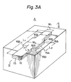
- Figure 3A is a perspective view of the structure of a main portion of a semiconductor laser according to a first embodiment of the present invention.
- Fig. 3B is a side-cross sectional view of the laser taken along line III-III of Fig. 3A.
- n +- type InP Indium Phosphorus
- an n-type InP buffer layer 12 is formed on an n +- type InP (Indium Phosphorus) substrate 11.
- An n-type InP clad layer 13 is formed on the n-type InP buffer layer 12.
- a corrugation 14 is formed in an n-type InGaAsP (Indium Gallium Arsecenic Phosphorus) optical guide layer 15 which is formed on the n-type InP clad layer 13.
- the corrugation 14 is also referred to as a diffraction grating.
- the n-type InGaAsP optical guide layer 15 can transfer light with the wavelength equal to 1.2 ⁇ m which corresponds to the forbibidden bandwidth of the layer 15.
- An InGaAsP (Indium Gallium Arsenic Phosphorus) active layer 16 is formed on the n-type InGaAsP optical guide layer 15.
- the InGaAsP active layer can generate light with the wavelength equal to 1.3 ⁇ m.
- the n-type InGaAsP optical guide layer 15 and the InGaAsP active layer 16 have, at their middle portions, expanded width portions 15A and 16A.
- the perspective view shown in Fig. 3A illustrates the just above mentioned structure. As can be seen from Fig. 3A, the n-type InGaAsP optical guide layer 15 and the InGaAsP active layer 16 are stripe-shaped. Referring back to Fig.
- a p-type InP clad layer 17 is further formed on the InGaAsP active layer 16. Finally, a p +- type InGaAsP contact layer 18 is formed on the p-type InP clad layer 17. An n side electrode plate 19 is formed under the n +- type InP substrate 11. A p-side electrode plate 20 is formed on the p +- type InGaAsP Contact layer 18.
- the direction of the thickness from the n side electrode plate 19 to the p-side electrode plate 20 is a first direction; the extending direction of the stripe-shaped optical guide layer 15 and the stripe-shaped active layer 16 is a second direction; and the direction of the width of the optical guide layer 15 or the active layer 16 is a third direction.
- the length of the active layer 16 in the second direction is L l ; and the length of the expanded width portion 15A or 16A in the second direction is L 2 which is shorter than L 1 .
- the corrugation 14 is formed uniformly without any shift.
- the expanded width portions 15A and 16A have, at their corners, tapered portions 15B and 16B over which the optical guide layer 15 and the active layer 16 gently extends.
- the tapered portions have their lengths in the second direction equal to L 3 -
- the expanded width portions 15A and 16A have their width W 2 in the third direction.
- the n side electrode plate 19 and the p side electrode plate 20 When an electric voltage is applied between the n side electrode plate 19 and the p side electrode plate 20, light is generated mainly in the active layer 16. The generated light conducts through the active layer 16 and its peripheral. In the region of the nonexpanded width portion of the active layer 16, the light conducts at a propagation constant B 1 . In the region of the expanded width portion 16A, the light conducts at another propagation constant S 2 .
- the formation of the expanded width portions can be easily realized by utilizing a mask.
- the shift of the corrugation is not necessary.
- the control of the thickness of the active layer 16 or the optical guide layer 15 is not so critical.
- Figure 4 is a graph explaining the phase shift of light in the structure shown in Fig. 3B. From the figure, it will be understood that the phase of light with the propagation constant B 2 delays by X/4 after the propagation through the length L 2 , in comparison with the phase of light with the propagation constant B 1 .
- the period A of the corrugation 14, in the secondary mode as an example is expressed as:
- differential propagation ⁇ B can be expressed as
- the width is gradually increased over the length L 3 .
- the four corners of the expanded width portion 16A are tormed so as to be tapered.
- the tapered portions 15B and 16B are tormed because due consideration must be given to occurrence of possible defects at the boundary region in the case ot a rapid increase in the width, which would detrimentally aftect the characteristics of the active layer 16 or the expanded width portion 16A. If no such problems would arise, the gently increased width portion could be eliminated, as shown by the broken line in the figure. Experiments showed that no trouble occurred even when the gently increased width portion was eliminated.
- Figs. 5A through 5D show the manufacturing steps of the laser shown in Fig. 3A.
- the n +- type InP sustrate 11, the n-type InP butfer layer 12, and the n-type InP clad layer 13 are formed.
- the corrugation 14 is uniformly formed. Since it is not necessary to form any shift portion in the corrugation 14, the manufacture ot the corrugation 14 is relatively easy.
- the device shown in Fig. 5A is subjected to crystal growth. Then, as shown in Fig. 5B, the n-type InGaAsP optical guide layer 15, the n-type InGaAsP active layer 16, the p-type InP clad layer 17, and the p +- type InGaAsP contact layer 18 are sequentially formed. Then, on the p +- type InGaAsP contact layer 18, a mask 21 made of silicon dioxide (Si0 2 ) is formed. The mask 21 is used to realize the stripe-shaped layers.
- Si0 2 silicon dioxide
- an etching process is carried out on the device shown in Fig. 5B, resulting in the clad layer 13, the optical guide layer 15, the active layer 16, the clad layer 17, and the contact layer 18 to be stripe-shaped.
- a p-type InP layer 22, an n-type InP layer 23, and a p-type InP layer 24 are formed on the etched portion by crystal growth.
- the semiconductor laser A shown in Fig. 3B is formed.
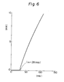
- Figure 6 is a graph showing the relationship between the light output and current in the embodiment explained with reference to Fig. 3A and Fig. 3B.
- the ordinate indicates the light output and the abscissa the current.
- the value of the threshold current I th is 28 mA.
- the light output rapidly rises after that value.
- Figure 7 is a graph showing the oscillation wavelength spectrum of the embodiment explained with reference to Fig. 3A and Fig. 3B.
- Figure 8 is a graph showing the oscillation wavelength spectrum in the case of the light output of the embodiment explained with reference to Fig. 3A and Fig. 3B being 8 mW.
- Figure 9 is a perspective view ot the structure of a semiconductor laser according to a second embodiment, of the present invention.
- the difference between the embodiment shown in Fig. 3A and the embodiment shown in Fig. 9 is that, in place of the expanded width portions 15A and 16A in the laser shown in Fig. 3A, narrowed width portions l5Aa and l6Aa are provided in the stripe-shaped optical guide layer 15 and in the stripe-shaped active layer 16.
- the width ot the narrowed width portion 15Aa and l6Aa is W 3 which is smaller than W l .
- the width W 3 is appropriately determined so as to shift the phase of the propagated light by exactly ⁇ /4.
- Figure 10 is a perspective view of the structure of a semiconductor laser according to a third embodiment of the present invention.
- the ditterence between the embodiment shown in Fig. 3A and the embodiment shown in Fig. 10 is that, in place of the two stripe-shaped layers 15 and 16 in the laser shown in Fig. 3A, only the active layer 16 having the expanded width portion 16A is made to be stripe-shaped.
- This structure also enables the shift ot the phase of the propagated light by exactly ⁇ /4, because most of the light is propagated through the active layer 16.
- Figure 11 is a perspective view of the structure of a semiconductor laser according to a fourth embodiment of the present invention.
- the difference between the embodiment shown in Fig. 9 and the embodiment shown in Fig. 11 is that, in place ot the two stripe-shaped layers 15 and 16 in the laser shown in Fig. 9, only the active layer 16 having the narrowed width portion l6Aa is made to be stripe-shaped.
- This structure also enables the shift ot the phase of the propagated light by exactly ⁇ /4.
- Figure 12A is a perspective view of the structure of a semiconductor laser according to a fifth embodiment of the present invention.
- Figure 12B is a side cross-sectional view of the laser taken along line XII-XII of Fig. 12A.
- the difference between the embodiment shown in Fig. 10 and the embodiment shown in Figs. 12A and 12B is that, in place of the expanded width portion 16A in the laser shown in Fig. 10, a recess portion (thin portion) l6Ab, having a thickness TH 1 smaller than the thickness TH 2 of the stripe-shaped active layer 16, is provided in place of the expanded width portion 16A.
- the formation of the thin portion l6Ab in the active layer 16 results in a different light propagation constant.
- ⁇ BL in this embodiment is - ⁇ /2.
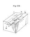
- Figure 13A is a perspective view of the structure of a semiconductor laser according to a sixth embodiment of the present invention.
- Figure 13B is a side cross-sectional view of the laser taken along line XIII-XI ll of Fig. 13A.
- a thick portion l6Ac having a thickness TH 3 larger than the thickness TH 2 of the stripe-shaped active layer 16, is provided in place of the thin portion l6Ab in the laser shown in Figs. 12A and 12B.
- the formation of the thick portion 16Ac in the active layer 16 results in a different light propagation constant.
- ⁇ BL in this embodiment is ⁇ /2.
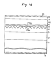
- Figure 14 is a side cross-sectional view of a semiconductor laser according to a seventh embodiment of the present invention.
- a second optical guide layer 140 is formed on the active layer 1 6.
- a portion 140A with a composition different from a composition in the other portion ot the second optical guide layer 140 is formed in the second optical guide layer 140.
- This selective formation of the portion 140A also results in a different propagation constant.
- a selective formation of a portion 15Ad with a composition different from a composition in the other portion in the optical guide layer 15 may also result in a different propagation constant.
- the semiconductor laser can stably oscillate at a monochromatic wavelength, i.e., the Bragg wavelength.
- the construction for enabling this i.e., for selectively creating the portion with the different propagation constant in a part of the light waveguide region is much easier compared with a conventional A/2 shift DFB semiconductor laser, as can be understood from the above embodiments, thus also making reproducibility excellent.
Applications Claiming Priority (2)
| Application Number | Priority Date | Filing Date | Title |
|---|---|---|---|
| JP210588/84 | 1984-10-09 | ||
| JP59210588A JPS6189690A (ja) | 1984-10-09 | 1984-10-09 | 半導体レ−ザ |
Publications (3)
| Publication Number | Publication Date |
|---|---|
| EP0178134A2 true EP0178134A2 (de) | 1986-04-16 |
| EP0178134A3 EP0178134A3 (en) | 1987-05-20 |
| EP0178134B1 EP0178134B1 (de) | 1990-10-03 |
Family
ID=16591801
Family Applications (1)
| Application Number | Title | Priority Date | Filing Date |
|---|---|---|---|
| EP85307130A Expired - Lifetime EP0178134B1 (de) | 1984-10-09 | 1985-10-04 | Halbleiterlaser |
Country Status (5)
| Country | Link |
|---|---|
| US (1) | US4726031A (de) |
| EP (1) | EP0178134B1 (de) |
| JP (1) | JPS6189690A (de) |
| KR (1) | KR890004646B1 (de) |
| DE (1) | DE3579991D1 (de) |
Cited By (2)
| Publication number | Priority date | Publication date | Assignee | Title |
|---|---|---|---|---|
| GB2185149B (en) * | 1985-12-18 | 1989-10-18 | Sony Corp | Distributed feedback semiconductor lasers |
| EP0546743A1 (de) * | 1991-12-12 | 1993-06-16 | Wisconsin Alumni Research Foundation | Phasenverschobener Halbleiterlaser mit verteilter Rückkoppelung |
Families Citing this family (19)
| Publication number | Priority date | Publication date | Assignee | Title |
|---|---|---|---|---|
| US4837775A (en) * | 1985-10-21 | 1989-06-06 | General Electric Company | Electro-optic device having a laterally varying region |
| FR2598862B1 (fr) * | 1986-05-16 | 1994-04-08 | Bouley Jean Claude | Laser a semi-conducteur a reaction distribuee et a longueur d'onde continument accordable. |
| US5340637A (en) * | 1986-09-16 | 1994-08-23 | Hitachi, Ltd. | Optical device diffraction gratings and a photomask for use in the same |
| JPS63244694A (ja) * | 1987-03-30 | 1988-10-12 | Sony Corp | 分布帰還形半導体レ−ザ |
| JP2768940B2 (ja) * | 1987-07-08 | 1998-06-25 | 三菱電機株式会社 | 単一波長発振半導体レーザ装置 |
| JPH0225086A (ja) * | 1988-07-13 | 1990-01-26 | Hitachi Ltd | 半導体レーザ装置 |
| JP2669045B2 (ja) * | 1989-04-20 | 1997-10-27 | 三菱電機株式会社 | 分布帰還型半導体レーザの製造方法 |
| DE3934865A1 (de) * | 1989-10-19 | 1991-04-25 | Siemens Ag | Hochfrequent modulierbarer halbleiterlaser |
| US5185759A (en) * | 1990-06-12 | 1993-02-09 | Kabushiki Kaisha Toshiba | Phase-shifted distributed feedback type semiconductor laser device |
| US5537432A (en) * | 1993-01-07 | 1996-07-16 | Sdl, Inc. | Wavelength-stabilized, high power semiconductor laser |
| DE4322164A1 (de) * | 1993-07-03 | 1995-01-12 | Ant Nachrichtentech | Optoelektronisches Bauelement mit Rückkopplungsgitter, mit axial quasi-kontinuierlich und nahezu beliebig variierbarem Gitterkopplungs-Koeffizienten, mit quasi-kontinuierlich axial verteilbarer Brechungsindex-Variation, sowie mit axial nahezu beliebig verteilbarer und variierbarer Phasenverschiebung |
| DE4322163A1 (de) * | 1993-07-03 | 1995-01-12 | Ant Nachrichtentech | Auf DFB- oder DBR-Gitter basierendes optoelektronisches Bauelement mit quasi-kontinuierlich axial verteilbarer Brechungsindex-Variation, mit axial beliebig verteilbarer und variierbarer Phasenverschiebung, sowie mit axial quasi-kontinuierlich variierbarem Gitter-Kopplungskoeffizienten |
| DE4432410B4 (de) * | 1994-08-31 | 2007-06-21 | ADC Telecommunications, Inc., Eden Prairie | Optoelektronisches Multi-Wellenlängen-Bauelement |
| JPH11307862A (ja) * | 1998-04-21 | 1999-11-05 | Nec Corp | 半導体レーザ |
| US6108469A (en) * | 1998-11-30 | 2000-08-22 | Lucent Technologies Inc | Wavelength selective resonant gratings |
| JP5233090B2 (ja) * | 2006-07-28 | 2013-07-10 | 沖電気工業株式会社 | キャリア抑圧光パルス列発生方法及びこの方法を実現するモード同期半導体レーザ |
| US7929580B2 (en) * | 2006-09-22 | 2011-04-19 | Alcatel-Lucent Usa Inc. | Inexpensive terahertz pulse wave generator |
| KR100842277B1 (ko) * | 2006-12-07 | 2008-06-30 | 한국전자통신연구원 | 반사형 반도체 광증폭기 및 수퍼 루미네센스 다이오드 |
| WO2021005700A1 (ja) * | 2019-07-09 | 2021-01-14 | 日本電信電話株式会社 | 半導体光素子 |
Citations (4)
| Publication number | Priority date | Publication date | Assignee | Title |
|---|---|---|---|---|
| DE2537093A1 (de) * | 1975-06-11 | 1977-01-13 | Hitachi Ltd | Halbleiterlaser und verfahren zu seiner herstellung |
| EP0000557A1 (de) * | 1977-08-01 | 1979-02-07 | Hitachi, Ltd. | Halbleiterlaser |
| JPS5763880A (en) * | 1980-10-04 | 1982-04-17 | Ikuo Suemune | Lateral distribution feedback type semiconductor laser |
| EP0149462B1 (de) * | 1984-01-09 | 1992-04-01 | Nec Corporation | Halbleiterlaser mit verteilter Rückkopplung |
Family Cites Families (1)
| Publication number | Priority date | Publication date | Assignee | Title |
|---|---|---|---|---|
| US4096446A (en) * | 1976-02-02 | 1978-06-20 | Bell Telephone Laboratories, Incorporated | Distributed feedback devices with perturbations deviating from uniformity for removing mode degeneracy |
-
1984
- 1984-10-09 JP JP59210588A patent/JPS6189690A/ja active Granted
-
1985
- 1985-10-04 EP EP85307130A patent/EP0178134B1/de not_active Expired - Lifetime
- 1985-10-04 DE DE8585307130T patent/DE3579991D1/de not_active Expired - Fee Related
- 1985-10-04 US US06/784,594 patent/US4726031A/en not_active Expired - Fee Related
- 1985-10-07 KR KR8507366A patent/KR890004646B1/ko not_active IP Right Cessation
Patent Citations (4)
| Publication number | Priority date | Publication date | Assignee | Title |
|---|---|---|---|---|
| DE2537093A1 (de) * | 1975-06-11 | 1977-01-13 | Hitachi Ltd | Halbleiterlaser und verfahren zu seiner herstellung |
| EP0000557A1 (de) * | 1977-08-01 | 1979-02-07 | Hitachi, Ltd. | Halbleiterlaser |
| JPS5763880A (en) * | 1980-10-04 | 1982-04-17 | Ikuo Suemune | Lateral distribution feedback type semiconductor laser |
| EP0149462B1 (de) * | 1984-01-09 | 1992-04-01 | Nec Corporation | Halbleiterlaser mit verteilter Rückkopplung |
Non-Patent Citations (5)
| Title |
|---|
| ELECTRONICS LETTERS, vol. 20, no. 2, 19th January 1984, pages 82-84, Hitchin, Herts., GB; K. TADA et al.: "Proposal of a distributed feedback laser with nonuniform stripe width for complete single-mode oscillation" * |
| ELECTRONICS LETTERS, vol. 20, no. 24, 22nd November 1984, pages 1016-1018, Stevenage, Herts., GB; H. SODA et al.: "GalnAsP/InP phase-adjusted distributed feedback lasers with a step-like nonuniform stripe width structure" * |
| ELEKTRONICS INTERNATIONAL, vol. 54, no. 23, November 1981, pages 68-70, New York, US; C. COHEN: "1.5um laser operates at 23 degree C" * |
| IEEE JOURNAL OF QUANTUM ELECTRONICS, vol. QE-12, no. 9, September 1976, pages 532-539, New York, US; H.A. HAUS et al.: "Antisymmetric taper of distributed feedback lasers" * |
| PATENTS ABSTRACTS of JAPAN, vol. 6, no. 140 (E-121)[1018], 29th July 1982; & JP-A-57 63 880 (IKUE SUEMUNE) 17.04.1982 * |
Cited By (3)
| Publication number | Priority date | Publication date | Assignee | Title |
|---|---|---|---|---|
| GB2185149B (en) * | 1985-12-18 | 1989-10-18 | Sony Corp | Distributed feedback semiconductor lasers |
| EP0546743A1 (de) * | 1991-12-12 | 1993-06-16 | Wisconsin Alumni Research Foundation | Phasenverschobener Halbleiterlaser mit verteilter Rückkoppelung |
| US5272714A (en) * | 1991-12-12 | 1993-12-21 | Wisconsin Alumni Research Foundation | Distributed phase shift semiconductor laser |
Also Published As
| Publication number | Publication date |
|---|---|
| JPS6189690A (ja) | 1986-05-07 |
| DE3579991D1 (de) | 1990-11-08 |
| KR890004646B1 (en) | 1989-11-21 |
| EP0178134B1 (de) | 1990-10-03 |
| EP0178134A3 (en) | 1987-05-20 |
| JPH0213942B2 (de) | 1990-04-05 |
| US4726031A (en) | 1988-02-16 |
Similar Documents
| Publication | Publication Date | Title |
|---|---|---|
| EP0178134B1 (de) | Halbleiterlaser | |
| EP0195425B1 (de) | Halbleiterlaser mit verteilter Rückkopplung | |
| EP0721240B1 (de) | Polarisationsmodenselektiver Halbleiterlaser, Modulationsverfahren und optisches Kommunikationssystem unter Verwendung dieses Lasers | |
| US5799119A (en) | Coupling of strongly and weakly guiding waveguides for compact integrated mach zehnder modulators | |
| EP0735635B1 (de) | Optischer Halbleitervorrichtung, Antriebsverfahren und optisches Kommunikationssystem | |
| EP0300790B1 (de) | Halbleiterlaser | |
| JPH0652820B2 (ja) | エッチング方法 | |
| EP0314490A2 (de) | Halbleiterlaser | |
| JP3198338B2 (ja) | 半導体発光装置 | |
| EP0125608A2 (de) | Halbleiterlaser in longitudinalem Einmodenbetrieb | |
| US4775980A (en) | Distributed-feedback semiconductor laser device | |
| EP0461632B1 (de) | Phasenverschobener Halbleiterlaser mit verteilter Rückkoppelung | |
| EP0285104B1 (de) | Halbleiterlaser mit verteilter Rückkopplung | |
| EP0717481A1 (de) | Halbleiterlaser, Modulationsverfahren und optisches Kommunikationssystem | |
| JP2002084033A (ja) | 分布帰還型半導体レーザ | |
| CN116207609A (zh) | 一种基于键合结构的温度不敏感型硅光发射芯片 | |
| JP3382471B2 (ja) | 半導体光デバイス及びそれを用いた光ネットワーク | |
| EP0155853B1 (de) | Resonatornahe Bereiche in einem Halbleiterlaser vom Typ VSIS | |
| JPH0431195B2 (de) | ||
| EP0269061A2 (de) | Optische Filtervorrichtung | |
| EP0274441B1 (de) | Halbleiterlaser mit verteilter Rückkopplung | |
| JPH0147031B2 (de) | ||
| WO2022269848A1 (ja) | 半導体レーザ | |
| KR100630514B1 (ko) | 전기 흡수 변조기 및 그러한 변조기를 제조하는 방법 | |
| JP3226072B2 (ja) | 偏波変調可能な半導体レーザとその使用法 |
Legal Events
| Date | Code | Title | Description |
|---|---|---|---|
| PUAI | Public reference made under article 153(3) epc to a published international application that has entered the european phase |
Free format text: ORIGINAL CODE: 0009012 |
|
| AK | Designated contracting states |
Kind code of ref document: A2 Designated state(s): DE FR GB |
|
| PUAL | Search report despatched |
Free format text: ORIGINAL CODE: 0009013 |
|
| AK | Designated contracting states |
Kind code of ref document: A3 Designated state(s): DE FR GB |
|
| 17P | Request for examination filed |
Effective date: 19871106 |
|
| 17Q | First examination report despatched |
Effective date: 19891115 |
|
| GRAA | (expected) grant |
Free format text: ORIGINAL CODE: 0009210 |
|
| AK | Designated contracting states |
Kind code of ref document: B1 Designated state(s): DE FR GB |
|
| ET | Fr: translation filed | ||
| REF | Corresponds to: |
Ref document number: 3579991 Country of ref document: DE Date of ref document: 19901108 |
|
| PLBE | No opposition filed within time limit |
Free format text: ORIGINAL CODE: 0009261 |
|
| STAA | Information on the status of an ep patent application or granted ep patent |
Free format text: STATUS: NO OPPOSITION FILED WITHIN TIME LIMIT |
|
| 26N | No opposition filed | ||
| PGFP | Annual fee paid to national office [announced via postgrant information from national office to epo] |
Ref country code: GB Payment date: 19920922 Year of fee payment: 8 |
|
| PGFP | Annual fee paid to national office [announced via postgrant information from national office to epo] |
Ref country code: FR Payment date: 19921028 Year of fee payment: 8 |
|
| PGFP | Annual fee paid to national office [announced via postgrant information from national office to epo] |
Ref country code: DE Payment date: 19921226 Year of fee payment: 8 |
|
| PG25 | Lapsed in a contracting state [announced via postgrant information from national office to epo] |
Ref country code: GB Effective date: 19931004 |
|
| GBPC | Gb: european patent ceased through non-payment of renewal fee |
Effective date: 19931004 |
|
| PG25 | Lapsed in a contracting state [announced via postgrant information from national office to epo] |
Ref country code: FR Effective date: 19940630 |
|
| PG25 | Lapsed in a contracting state [announced via postgrant information from national office to epo] |
Ref country code: DE Effective date: 19940701 |
|
| REG | Reference to a national code |
Ref country code: FR Ref legal event code: ST |