EP0177750B1 - Kontaktanordnung für Vakuumschalter - Google Patents
Kontaktanordnung für Vakuumschalter Download PDFInfo
- Publication number
- EP0177750B1 EP0177750B1 EP85111118A EP85111118A EP0177750B1 EP 0177750 B1 EP0177750 B1 EP 0177750B1 EP 85111118 A EP85111118 A EP 85111118A EP 85111118 A EP85111118 A EP 85111118A EP 0177750 B1 EP0177750 B1 EP 0177750B1
- Authority
- EP
- European Patent Office
- Prior art keywords
- contact
- faces
- arc
- arc burning
- axial direction
- Prior art date
- Legal status (The legal status is an assumption and is not a legal conclusion. Google has not performed a legal analysis and makes no representation as to the accuracy of the status listed.)
- Expired
Links
Images
Classifications
-
- H—ELECTRICITY
- H01—ELECTRIC ELEMENTS
- H01H—ELECTRIC SWITCHES; RELAYS; SELECTORS; EMERGENCY PROTECTIVE DEVICES
- H01H33/00—High-tension or heavy-current switches with arc-extinguishing or arc-preventing means
- H01H33/60—Switches wherein the means for extinguishing or preventing the arc do not include separate means for obtaining or increasing flow of arc-extinguishing fluid
- H01H33/66—Vacuum switches
- H01H33/664—Contacts; Arc-extinguishing means, e.g. arcing rings
- H01H33/6644—Contacts; Arc-extinguishing means, e.g. arcing rings having coil-like electrical connections between contact rod and the proper contact
Definitions
- the present invention relates to a contact arrangement for vacuum switches according to the preamble of claim 1.
- a contact arrangement is known from US Pat. No. 4,196,327.
- current loops are arranged behind the switching pieces, which generate areas of high and areas of low magnetic field strength in the axial direction in the contact piece and in the contact areas. Adjacent areas of high magnetic field strength in some cases have an opposite polarity of the field strength.
- Vacuum switches of this type are distinguished by rapid dielectric reconsolidation of the switching path after the zero current crossing (sheet break).
- This advantage of the vacuum switch can with unfavorable circuit data or electrical conditions in the network, for. B. when switching off starting motors, have a negative impact. This can lead to premature zero current crossings with high steepness, which leads to phenomena that are referred to in the literature as "multiple reignitions" and can essentially lead to disruptive overvoltages at switch-off currents ⁇ 1 kA in the network.
- the switching path is influenced in accordance with the prior art in such a way that the tear-off current strength is kept small, whereby the overvoltages are generally reduced.
- a so-called “low surge material”. include, for example, chrome-copper composite materials with the addition of bismuth or tellurium. Such materials, however, have only a relatively small maximum switching capacity, in particular because of their high vapor pressure.
- the object on which the present invention is based is to provide a contact arrangement which, on the one hand, has a sufficiently slow re-solidification of the dielectric when switching off currents which are approximately equal to or less than the nominal current, and on the other hand has a high switching capacity at higher currents guaranteed.
- the invention is based on the knowledge that a metal vapor arc in the vacuum interrupter under the influence of an axial magnetic field after ignition within a commutation time t o , which decreases with increasing current and is, for example, about 3 ms at 10 kA, into a diffuse burning State changes, specifically in contact areas in which the specific induction B z / 1 caused by the axial magnetic field component reaches a minimum value.
- the arc voltage is many times lower than the value of the arc voltage in a contracted arc.
- a corresponding shape and arrangement ensures that the arc is drawn first in the contact areas and that is in the low-surge range when the contacts are separated.
- the concentratedly burning arc quickly shifts within t o to the areas of maximum magnetic field strength, whereby depending on the local field distribution it dissolves into a diffuse arc or into several diffusely burning partial arcs. There, as already known, it burns with a greatly reduced arc voltage on contact surfaces with a high load capacity. This prevents that the contact faces which consist of a so-called low-surge-material, are thermally overloaded and ensures that the sheet night t o burns in the field of appropriate for high switching performance arcing surfaces and thus ensures a high breaking capacity of the contact assembly.
- the current loops mentioned in the claim can be attached to one or both contacts or otherwise fixed in their position relative to the contacts so that their magnetic field at the points of the contact surfaces, which are made of low-surge contact material, is significantly smaller than in the arc burners surfaces with highly resilient contact material. As long as this condition is met, any form of current loop can be used.
- An advantageous embodiment of the contact arrangement according to the invention consists in that the contact surfaces, but not the arcing surfaces, of a contact piece can be brought into contact with the corresponding surfaces of the second contact piece. This ensures in a simple manner that the arc is only drawn in the area of the contact surfaces.
- An embodiment with only one arc burning surface, in which only a diffuse arc arises, is provided in that the contact surface represents a circular ring and in that the arc burning surface concentrically adjoins this circular ring in the interior of this circular ring.
- the arc burning surface can completely fill the circular ring formed by the contact surfaces or can itself be designed in a ring shape, in both cases there is a diffusely burning arc which fills the entire arc burning surface.
- An embodiment with a plurality of diffusely burning arcs is achieved in that the contact surface represents a circular disk concentric to the contact axis and in that the arcing surfaces lie on a ring surrounding the contact surface.
- This embodiment is particularly advantageously used in conjunction with generation of the axial magnetic field by conductor loops if the conductor loops are arranged on the side of the contact piece facing away from the contact surface and, such as, for. B. from US-PS 4,196,327, each include only one sector of an annulus.
- field-free means free of the axial field, which is caused by the current in the conductor loop.
- two or more arcing surfaces can be generated particularly easily on the ring, the arcing surfaces being penetrated by axial magnetic fields of different field directions.
- a diffuse arc in the focal areas is guaranteed if the current-related, specific field strength in the axial direction in the contact areas is below and in the arc focal areas above 1.5 pT / A.
- the value of 3 jj.T / A should at least be reached in the areas of maximum field strength of the arc burning surfaces so that the arc burning voltage reaches its minimum.
- the sheet on the location moves to the arc ignition at current levels above the value is from which to expect the occurrence of multiple re-ignitions within t o in the arc burning faces and merges into a diffuse burning state.
- the diffuse arc burns evenly, its burning voltage is several times lower than that of a contracted arc. This advantage is particularly important for currents of more than 10 kA, in which the arc burns contracted without an axial magnetic field and, based on experience, has an unstable behavior.
- Chrome-copper which guarantees a high switching capacity, is suitable as contact material for the arc burners.
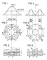
- FIGS. 1 and 4 show the distribution of the specific induction in the axial direction for two exemplary embodiments
- FIGS. 2 and 5 show the associated contact surfaces and arcing surfaces schematically
- FIGS. 3 and 6 each show an exemplary embodiment of a corresponding contact piece.
- an annular contact surface 1 with a truncated cone-shaped transmission region 3 encloses an arc burning surface 2.
- a low-surge material is contained in the contact surface 1, so that no disturbing current chopping can occur there.
- the arc burning surface 2 consists of a contact material for high breaking capacities, for example chrome-copper.
- This contact advantageously has the structure shown in FIG. 3, in which a contact carrier 4 is made pot-shaped from an electrically highly conductive material and has slots 6 in its contact carrier wall which form a relatively large angle with the axis of rotation 7, as a result of which an axial magnetic field component is produced. This angle is approximately 70 °, for example.
- the webs 8 remaining between the slots 6 are made of a material with low electrical conductivity, e.g. B. with a rotating body R, made of ceramic or metal relieved or supported so that the contact has the necessary mechanical strength.
- the webs 8 here form sections of conductor loops for generating a magnetic field with an axial component.
- the axial component of the magnetic field has a current-related minimum induction B z (min) / 1 of 1.5 ⁇ / A in the arcing area 2 on a contact disk 5, which is made of a material with a large switching capacity.
- the adjoining transition surface 3 and the contact surface 1 are formed from a ring made of low-surge material, the dimensions of which ensure that the current-related minimum induction B z (min) / 1 is exceeded within the transition zone.
- This ring made of low-surge material and the contact disk 5 are expediently provided with radial slots S in order to avoid eddy current formation in the contact, which can reduce the axial field component to a remainder of approximately 30%.
- This embodiment forms a diffusely burning arcing area which fills the entire arcing area 2.
- the maximum specific induction B z (max) / 1 is in the region of the axis of rotation of the contact. It exceeds the value 3 (JLT / A (unipole contact).
- the second embodiment according to the Fig. 4 to 6 has a disc-shaped contact surface 9 and an adjoining, concentric ring 10 which is made of a material for high switching powers, for. B. chrome copper. Behind the ring 10 there are conductor loops which are traversed by parts of the current flowing through the contact and which fix arc-burning surfaces 11 to 14 on the contact ring, in which the minimum value for the specific induction B z (min) / l is exceeded. The field between adjacent arc burning surfaces 11 to 14 changes its direction (multipole contact).
- a simple embodiment of such a contact is provided in that the contact ring 10 is part of a contact disk 15 and in that a disk 20 made of low-surge material, which forms the contact surface 9, is applied concentrically to the contact disk 15.
- the magnetic field acting in the axial direction is formed by a winding arrangement known per se in the form of a spoke wheel, with 16, 17 mutually perpendicular spokes, which lead to a ring 18.
- the spokes 16 and 17 are supported against one another in the axial direction by a support body 19 with low electrical conductivity. The current flows from the spoke 16 through the ring 18 into the spoke 17 and from there into the contact disk 15.
- the minimum value of the specific induction is reached in the arcing areas, but the peak value of the specific induction is lower than in example 1. Since in this arrangement the migration of the arc into the arcing areas is favored by the current forces which cause the arc in the radial direction pushing outward, a certain distance between the contact surface 9 and the arc burning surfaces 11 to 14 is also permissible in this example.
Description
- Die vorliegende Erfindung betrifft eine Kontaktanordnung für Vakuumschalter nach dem Oberbegriff des Patentanspruchs 1. Eine derartige Kontaktanordnung ist aus der US-PS 4 196 327 bekannt. Dort werden hinter den Schaltstücken Stromschleifen angeordnet, welche im Kontaktstück und in den Kontaktflächen Bereiche hoher und Bereiche geringer magnetischer Feldstärke in axialer Richtung erzeugen. Benachbarte Bereiche hoher magnetischer Feldstärke weisen dabei teilweise eine entgegengesetzte' Polarität der Feldstärke auf.
- Derartige Vakuumschalter zeichnen sich durch eine schnelle dielektrische Wiederverfestigung der Schaltstrecke nach dem Strom-Nulldurchgang (Bogenabriß) aus. Dieser Vorteil der Vakuumschalter kann sich bei ungünstigen Kreisdaten bzw. elektrischen Verhältnissen im Netz, z. B. beim Abschalten von anlaufenden Motoren, negativ auswirken. Dabei können nämlich frühzeitige Strom-Nulldurchgänge mit hoher Steilheit entstehen, welche zu Erscheinungen führen, die in der Literatur als « multiple Wiederzündungen » bezeichnet werden und im wesentlichen bei Ausschaltströmen < 1 kA im Netz zu störenden Überspannungen führen können.
- Um diesen Effekt klein zu halten, wird nach dem Stand der Technik die Schaltstrecke so beeinflußt, daß die Abreißstromstärke klein gehalten wird, wodurch nach allgemeiner Ansicht die Überspannungen vermindert werden. Dies wird durch ein entsprechend ausgewähltes Kontaktmaterial, ein sogenanntes « Low-surge-material » erreicht. Hierzu zählen beispielsweise Chrom-Kupfer-Verbundmaterialien mit Zusatz von Wismut oder Tellur. Solche Materialien weisen jedoch insbesondere wegen ihres großen Dampfdruckes nur eine relativ kleine maximale Schaltleistung auf. Beim Ausschalten von Strömen, die beispielsweise mehr als 10 kA betragen, treten auch hier leicht Wiederzündungen auf ; das Ausschalten gelingt nicht mit Sicherheit.
- Aus der GB-PS 15 98 397 ist bekannt, bei Kontakten mit rotierendem Lichtbogen den Kontakt in einen Hauptkontaktteil und einen Hilfskontaktteil aufzuteilen, wobei die Hilfskontaktteile der beiden Schaltstücke beim Schließen des Schalters miteinander in Berührung gebracht werden, die Hauptkontaktteile aber nicht. Aufgrund der Stromführung in dem dort beschriebenen Kontakt soll der Lichtbogen vom Hilfskontaktteil auf den Hauptkontaktteil abgedrängt werden. Der Hilfskontaktteil weist ein Low-surge-material auf, der Hauptkontaktteil ein Material für große Schaltleistung. Durch die spezielle Formgebung soll bei den dort beschriebenen Kontakten ein schwacher Strom nur im Bereich der Hilfskontakte einen Lichtbogen erzeugen, während der Lichtbogen eines starken Stromes auf den Hauptkontaktteil wandert, wo er ein Material hoher Ausschaltleistung vorfindet. Die elektromotorische Kraft, die auf den Lichtbogen wirkt, soll durch den Stromfluß über die Kontakte entstehen, vergleiche Fig. 1a und 1b und Seite 6 der Beschreibung.
- Auf Grund des instabilen Verhaltens des bei größeren Stromstärken kontrahiert brennenden Lichtbogens ist jedoch nicht immer gewährleistet, daß dieser die Hilfskontaktflächen so schnell verläßt, daß eine thermische Überlastung derselben mit Sicherheit ausgeschlossen ist.
- Die Aufgabe, die der vorliegenden Erfindung zugrunde liegt, besteht darin, eine Kontaktanordnung anzugeben, welche einerseits beim Ausschalten von Strömen, die etwa gleich dem oder kleiner als der Nennstrom sind, eine genügend langsame Wiederverfestigung des Dielektrikums aufweist und andererseits bei höheren Strömen eine große Schaltleistung gewährleistet.
- Diese Aufgabe wird bei einem Schaltkontakt gemäß dem Oberbegriff durch die kennzeichnenden Merkmale des Patentanspruchs 1 gelöst.
- Die Erfindung beruht auf der Erkenntnis, daß ein Metalldampf-Lichtbogen in der Vakuumschaltröhre unter dem Einfluß eines axialen Magnetfeldes nach dem Zünden innerhalb einer Kommutierungszeit to, welche mit wachsender Stromstärke sinkt und bei 10 kA beispielsweise ca. 3 ms beträgt, in einen diffus brennenden Zustand übergeht, und zwar in Kontaktbereichen, in denen die durch die axiale Magnetfeldkomponente hervorgerufene spezifische Induktion Bz/1 einen Mindestwert erreicht. Im diffus brennenden Zustand liegt die Bogenbrennspannung um ein Vielfaches unter dem Wert der Brennspannung in einem kontrahierten Bogen. In der erfindungsgemäßen Kontaktanordnung wird durch eine entsprechende Form und Anordnung gewährleistet, daß der Lichtbogen beim Trennen der Kontakte zuerst in den Kontaktflächen und das heißt im Low-surge-Bereich gezogen wird. Unter der Wirkung des axialen Magnetfeldes verlagert sich der konzentriert brennende Bogen schnell, innerhalb to in die Bereiche maximaler Magnetfeldstärke, wobei er sich je nach der lokalen Feldverteilung in einen diffusen Lichtbogen oder in mehrere diffus brennende Teilbögen auflöst. Dort brennt er, wie bereits bekannt, mit stark verringerter Bogenbrennspannung auf Kontaktflächen mit hoher Belastbarkeit. Somit wird verhindert, daß die Kontaktflächen, welche aus einem sogenannten Low-surge-material bestehen, thermisch überlastet werden und gewährleistet, daß der Bogen nacht to im Bereich der für hohe Schaltleistungen geeigneten Lichtbogenbrennflächen brennt und damit ein hohes Ausschaltvermögen der Kontaktanordnung gewährleistet.
- Die im Patentanspruch genannten Stromschleifen können an einem oder beiden Kontakten angebracht oder auf andere Weise in ihrer Lage gegenüber den Kontakten so fixiert sein, daß ihr Magnetfeld in den Punkten der Kontaktflächen, welche aus Low-surge Kontaktmaterial bestehen, wesentlich kleiner ist als in den Lichtbogenbrennflächen mit hoch belastbarem Kontaktmaterial. Solange diese Bedingung erfüllt ist, können beliebige Formen von Stromschleifen eingesetzt werden.
- Eine vorteilhafte Ausführungsform der erfindungsgemäßen Kontaktanordnung besteht darin, daß die Kontaktflächen, nicht aber die Lichtbogenbrennflächen, eines Kontaktstückes mit den entsprechenden Flächen des zweiten Kontaktstückes in Berührung gebracht werden können. So ist auf einfache Weise gewährleistet, daß der Lichtbogen nur im Bereich der Kontaktflächen gezogen wird. Eine Ausführungsform mit nur einer Lichtbogenbrennfläche, in der nur ein diffuser Lichtbogen entsteht, ist gegeben, indem die Kontaktfläche einen Kreisring darstellt und indem die Lichtbogenbrennfläche sich konzentrisch im Inneren dieses Kreisringes an diesen anschließt. Dabei kann die Lichtbogenbrennfläche den durch die Kontaktflächen gebildeten Kreisring vollständig ausfüllen oder selbst ringförmig gestaltet sein, in beiden Fällen ergibt sich ein diffus brennender Lichtbogen, der die gesamte Lichtbogenbrennfläche ausfüllt. Eine Ausführungsform mit mehreren diffus brennenden Lichtbögen wird erreicht, indem die Kontaktfläche eine zur Kontaktachse konzentrische Kreisscheibe darstellt und' indem die Lichtbogenbrennflächen auf einem die Kontaktfläche umgebenden Ring liegen. Diese Ausführung ist besonders vorteilhaft in Verbindung mit einer Erzeugung des axialen Magnetfeldes durch Leiterschleifen einsetzbar, wenn die Leiterschleifen auf der von der Kontaktfläche abgewandten Seite des Kontaktstückes angeordnet sind und, wie z. B. aus der US-PS 4,196.327 bekannt, jeweils nur einen Sektor eines Kreisringes umfassen. In diesem Fall ergeben sich feldfreie Zonen in der Mitte des Kreisringes und im Bereich der Begrenzung der Sektoren. Feldfrei heißt in diesem Zusammenhang frei vom Axialfeld, welches durch den Strom in der Leiterschleife hervorgerufen wird. Bei dieser Ausführungsform können besonders einfach zwei oder mehr Lichtbogenbrennflächen auf dem Ring erzeugt werden, wobei die Lichtbogenbrennflächen von axialen Magnetfeldern unterschiedlicher Feldrichtung durchsetzt werden.
- Ein diffuser Lichtbogen in den Brennflächen ist gewährleistet, wenn die strombezogene, spezifische Feldstärke in axialer Richtung in den Kontaktflächen unter und in den Lichtbogenbrennflächen über 1,5 p-T/A liegt. Dabei sollte in den Bereichen maximaler Feldstärke der Lichtbogenbrennflächen der Wert 3 jj.T/A zumindest erreicht werden, damit die Bogenbrennspannung ihr Minimum erreicht. In einer derartigen Ausführungsform wandert der Bogen vom Ort der Bogenzündung bei Stromstärken oberhalb des Wertes, ab welchem mit dem Auftreten von multiplen Wiederzündungen zu rechnen ist, innerhalb to in die Lichtbogenbrennflächen und geht in einen diffus brennenden Zustand über.
- Der diffuse Lichtbogen brennt gleichmäßig, seine Brennspannung ist um ein Mehrfaches geringer als die eines kontrahierten Lichtbogens. Dieser Vorteil kommt insbesondere bei Strömen von mehr als 10 kA zum Tragen, bei denen der Lichtbogen ohne ein axiales Magnetfeld kontrahiert brennt und erfahrungsgemäß ein unstabiles Verhalten aufweist.
- Als Kontaktmaterial für die Lichtbogenbrennflächen eignet sich Chrom-Kupfer, welches eine hohe Schaltleistung gewährleistet.
- Die Erfindung wird nun anhand von sechs Figuren näher erläutert. Die Fig. 1 und 4 zeigen die Verteilung der spezifischen Induktion in axialer Richtung für zwei Ausführungsbeispiele, die Fig. 2 und 5 zeigen die zugehörigen Kontaktflächen und Lichtbogenbrennflächen schematisch, die Fig. 3 und 6 zeigen je ein Ausführungsbeispiel eines entsprechenden Kontaktstückes.
- Im ersten Ausführungsbeispiel gemäß den Fig. 1 bis 3 umschließt eine ringförmige Kontaktfläche 1 mit einem kegelstumpfförmigen Übertragungsbereich 3 eine Lichtbogenbrennfläche 2. In der Kontaktfläche 1 ist ein Low-surge-material enthalten, so daß dort kein störender Stromabriß (current chopping) entstehen kann. Die Lichtbogenbrennfläche 2 besteht aus einem Kontaktwerkstoff für große Ausschaltleistungen, beispielsweise Chrom-Kupfer. Dieser Kontakt weist vorteilhaft den in Fig. 3 gezeigten Aufbau auf, in dem ein Kontaktträger 4 aus einem elektrisch gut leitfähigen Material topfförmig ausgebildet ist und in seiner Kontaktträgerwand Schlitze 6 aufweist, welche mit der Rotationsachse 7 einen relativ großen Winkel bilden, wodurch eine axiale Magnetfeldkomponente erzeugt wird. Dieser Winkel beträgt beispielsweise etwa 70°. Die zwischen den Schlitzen 6 verbleibenden Stege 8 werden mit einem Material geringer elektrischer Leitfähigkeit, z. B. mit einem Rotationskörper R, aus Keramik oder Metall entlastet oder abgestützt, damit der Kontakt die notwendige mechanische Festigkeit besitzt. Die Stege 8 bilden hier Teilstücke von Leiterschleifen zur Erzeugung eines Magnetfeldes mit einer axialen Komponente. Die axiale Komponente des Magnetfeldes weist in der Lichtbogenbrennfläche 2 auf einer Kontaktscheibe 5, die aus einem Material mit großem Schaltvermögen besteht, eine strombezogene Mindestinduktion Bz(min)/1 von 1,5 µ/A auf. Die daran anschließende Übergangsfläche 3 und die Kontaktfläche 1 sind aus einem Ring aus Low-surge-material gebildet, dessen Abmessungen gewährleisten, daß innerhalb der Übergangszone die strombezogene Mindestinduktion Bz(min)/1 überschritten ist. Dieser Ring aus Low-surge-material und die Kontaktscheibe 5 sind zweckmäßigerweise mit radialen Schlitzen S versehen, um eine Wirbelstrombildung im Kontakt, welche die axiale Feldkomponente bis auf einen Rest von etwa 30 % reduzieren kann, zu vermeiden. Diese Ausführungsform bildet einen diffus brennenden Lichtbogenbereich, der die gesamte Lichtbogenbrennfläche 2 ausfüllt. Die maximale spezifische Induktion Bz(max)/1 liegt hierbei im Bereich der Rotationsachse des Kontaktes. Sie überschreitet den Wert 3 (JLT/A (Unipolkontakt).
- Das zweite Ausführungsbeispiel gemäß den Fig. 4 bis 6 weist eine scheibenförmige Kontaktfläche 9 und einen daran anschließenden, konzentrischen Ring 10 auf, welcher aus einem Material für hohe Schaltleistungen, z. B. Chrom-Kupfer, besteht. Hinter dem Ring 10 sind Leiterschleifen angeordnet, welche von Teilen des durch den Kontakt fließenden Stromes durchflossen werden und auf dem Kontaktring Lichtbogenbrennflächen 11 bis 14 festlegen, in denen der Mindestwert für die spezifische Induktion Bz(min)/l überschritten ist. Dabei ändert das Feld zwischen jeweils benachbarten Lichtbogenbrennflächen 11 bis 14 seine Richtung (Multipolkontakt).
- Eine einfache Ausführungsform eines derartigen Kontaktes ist gegeben, indem der Kontaktring 10 Teil einer Kontaktscheibe 15 ist und indem auf die Kontaktscheibe 15 konzentrisch eine Scheibe 20 aus Low-surge-material aufgebracht ist, welche die Kontaktfläche 9 bildet. Das in axialer Richtung wirkende Magnetfeld wird durch eine an sich bekannte Windungsanordnung in der Form eines Speichenrades gebildet, wobei mit 16, 17 zueinander senkrechte Speichen bezeichnet sind, welche zu einem Ring 18 führen. Die Speichen 16 und 17 sind durch einen Stützkörper 19 mit geringer elektrischer Leitfähigkeit in axialer Richtung gegeneinander abgestützt. Der Strom fließt von der Speiche 16 durch den Ring 18 in die Speiche 17 und von dort in die Kontaktscheibe 15.
- Bei dieser Ausführungsform wird in den Lichtbogenbrennflächen der Minimalwert der spezifischen Induktion erreicht, der Spitzenwert der spezifischen Induktion liegt aber tiefer als bei Beispiel 1. Da bei dieser Anordnung die Wanderung des Lichtbogens in die Lichtbogenbrennflächen durch die Stromkräfte begünstigt wird, die den Lichtbogen in radialer Richtung nach außen drängen, ist bei diesem Beispiel auch ein gewisser Abstand zwischen der Kontaktfläche 9 und den Lichtbogenbrennflächen 11 bis 14 zulässig.
Claims (7)
Applications Claiming Priority (2)
| Application Number | Priority Date | Filing Date | Title |
|---|---|---|---|
| DE3435815 | 1984-09-28 | ||
| DE3435815 | 1984-09-28 |
Publications (2)
| Publication Number | Publication Date |
|---|---|
| EP0177750A1 EP0177750A1 (de) | 1986-04-16 |
| EP0177750B1 true EP0177750B1 (de) | 1989-03-15 |
Family
ID=6246705
Family Applications (1)
| Application Number | Title | Priority Date | Filing Date |
|---|---|---|---|
| EP85111118A Expired EP0177750B1 (de) | 1984-09-28 | 1985-09-03 | Kontaktanordnung für Vakuumschalter |
Country Status (4)
| Country | Link |
|---|---|
| US (1) | US4727228A (de) |
| EP (1) | EP0177750B1 (de) |
| JP (1) | JPS6185733A (de) |
| DE (1) | DE3568902D1 (de) |
Cited By (1)
| Publication number | Priority date | Publication date | Assignee | Title |
|---|---|---|---|---|
| DE4013903A1 (de) * | 1990-04-25 | 1990-11-22 | Slamecka Ernst | Magnetfeld-kontaktanordnung fuer vakuumschalter |
Families Citing this family (5)
| Publication number | Priority date | Publication date | Assignee | Title |
|---|---|---|---|---|
| US4837121A (en) * | 1987-11-23 | 1989-06-06 | Olin Hunt Specialty Products Inc. | Thermally stable light-sensitive compositions with o-quinone diazide and phenolic resin |
| US4970287A (en) * | 1987-11-23 | 1990-11-13 | Olin Hunt Specialty Products Inc. | Thermally stable phenolic resin compositions with ortho, ortho methylene linkage |
| DE4214550A1 (de) * | 1992-04-29 | 1993-11-04 | Siemens Ag | Vakuumschaltroehre |
| US5438174A (en) * | 1993-11-22 | 1995-08-01 | Eaton Corporation | Vacuum interrupter with a radial magnetic field |
| US6747233B1 (en) | 2001-12-28 | 2004-06-08 | Abb Technology Ag | Non-linear magnetic field distribution in vacuum interrupter contacts |
Family Cites Families (5)
| Publication number | Priority date | Publication date | Assignee | Title |
|---|---|---|---|---|
| US3980850A (en) * | 1974-12-19 | 1976-09-14 | Westinghouse Electric Corporation | Vacuum interrupter with cup-shaped contact having an inner arc controlling electrode |
| JPS58810B2 (ja) * | 1976-12-06 | 1983-01-08 | 株式会社日立製作所 | 真空しや断器 |
| JPS53147270A (en) * | 1977-05-27 | 1978-12-21 | Mitsubishi Electric Corp | Vacuum circuit breaker |
| NL168361C (nl) * | 1977-12-05 | 1982-03-16 | Hazemeijer Bv | Elektrische vacuumschakelaar. |
| CA1236868A (en) * | 1983-03-15 | 1988-05-17 | Yoshiyuki Kashiwagi | Vacuum interrupter |
-
1985
- 1985-08-22 US US06/768,148 patent/US4727228A/en not_active Expired - Fee Related
- 1985-09-03 DE DE8585111118T patent/DE3568902D1/de not_active Expired
- 1985-09-03 EP EP85111118A patent/EP0177750B1/de not_active Expired
- 1985-09-26 JP JP60213608A patent/JPS6185733A/ja active Pending
Cited By (1)
| Publication number | Priority date | Publication date | Assignee | Title |
|---|---|---|---|---|
| DE4013903A1 (de) * | 1990-04-25 | 1990-11-22 | Slamecka Ernst | Magnetfeld-kontaktanordnung fuer vakuumschalter |
Also Published As
| Publication number | Publication date |
|---|---|
| DE3568902D1 (en) | 1989-04-20 |
| EP0177750A1 (de) | 1986-04-16 |
| JPS6185733A (ja) | 1986-05-01 |
| US4727228A (en) | 1988-02-23 |
Similar Documents
| Publication | Publication Date | Title |
|---|---|---|
| DE4002933C2 (de) | ||
| DE3227482C2 (de) | ||
| EP0104384A1 (de) | Kontaktanordnung für Vakuumschalter | |
| EP0062186B1 (de) | Kontaktanordnung für Vakuumschalter | |
| DE3407088A1 (de) | Kontaktanordnung fuer vakuumschalter | |
| DE112010005149B4 (de) | Vakuum-schalter | |
| EP0381843A2 (de) | Schaltkontakt | |
| DE19856939A1 (de) | Schaltungsanordnung zum Schutz von elektrischen Installationen gegen Überspannungsereignisse | |
| DE60223766T2 (de) | Kontaktanordnung für einen Vakuumschalter und Vakuumschalter mit einer solchen Kontaktanordnung | |
| EP0177750B1 (de) | Kontaktanordnung für Vakuumschalter | |
| EP0073925A1 (de) | Kontaktanordnung für Vakuumschalter | |
| DE10253866A1 (de) | Kontaktstück mit abgerundeten Schlitzkanten | |
| DE2048506A1 (de) | Vakuumschalter | |
| EP1198812B1 (de) | Kontaktanordnung für eine vakuumschaltröhre | |
| DE60226347T2 (de) | Nichtlineare magnetfeldverteilung in vakuumunterbrecherkontakten | |
| EP1039495B1 (de) | Verfahren zur Strombegrenzung in Niederspannungsnetzen, zugehörige Anordnung sowie spezielle Verwendung dieser Anordnung | |
| DE2356515C2 (de) | Elektrodynamische Schaltvorrichtung wie Relais, Schütz od.dgl. | |
| EP0734580B1 (de) | Hochspannungs-leistungsschalter mit einer feldelektrode | |
| DE19957228B4 (de) | Kontaktanordnung für eine Vakuumschaltkammer | |
| EP0225562A1 (de) | Vakuumschaltröhre | |
| DE3332092A1 (de) | Kontaktanordnung fuer eine vakuumschaltroehre | |
| EP0203367A1 (de) | Kontaktanordnung für Vakuumschalter | |
| DE2902489A1 (de) | Kontaktanordnung fuer vakuumschalter | |
| DE2546376A1 (de) | Kontakt fuer vakuumschalter | |
| DE2822510A1 (de) | Vakuumschutzschalter |
Legal Events
| Date | Code | Title | Description |
|---|---|---|---|
| PUAI | Public reference made under article 153(3) epc to a published international application that has entered the european phase |
Free format text: ORIGINAL CODE: 0009012 |
|
| AK | Designated contracting states |
Kind code of ref document: A1 Designated state(s): CH DE FR GB LI |
|
| 17P | Request for examination filed |
Effective date: 19861010 |
|
| 17Q | First examination report despatched |
Effective date: 19880518 |
|
| GRAA | (expected) grant |
Free format text: ORIGINAL CODE: 0009210 |
|
| AK | Designated contracting states |
Kind code of ref document: B1 Designated state(s): CH DE FR GB LI |
|
| GBT | Gb: translation of ep patent filed (gb section 77(6)(a)/1977) | ||
| REF | Corresponds to: |
Ref document number: 3568902 Country of ref document: DE Date of ref document: 19890420 |
|
| ET | Fr: translation filed | ||
| PLBE | No opposition filed within time limit |
Free format text: ORIGINAL CODE: 0009261 |
|
| STAA | Information on the status of an ep patent application or granted ep patent |
Free format text: STATUS: NO OPPOSITION FILED WITHIN TIME LIMIT |
|
| 26N | No opposition filed | ||
| PGFP | Annual fee paid to national office [announced via postgrant information from national office to epo] |
Ref country code: GB Payment date: 19910822 Year of fee payment: 7 |
|
| PGFP | Annual fee paid to national office [announced via postgrant information from national office to epo] |
Ref country code: DE Payment date: 19911127 Year of fee payment: 7 |
|
| PGFP | Annual fee paid to national office [announced via postgrant information from national office to epo] |
Ref country code: CH Payment date: 19911216 Year of fee payment: 7 |
|
| PG25 | Lapsed in a contracting state [announced via postgrant information from national office to epo] |
Ref country code: GB Effective date: 19920903 |
|
| PGFP | Annual fee paid to national office [announced via postgrant information from national office to epo] |
Ref country code: FR Payment date: 19920917 Year of fee payment: 8 |
|
| PG25 | Lapsed in a contracting state [announced via postgrant information from national office to epo] |
Ref country code: LI Effective date: 19920930 Ref country code: CH Effective date: 19920930 |
|
| GBPC | Gb: european patent ceased through non-payment of renewal fee |
Effective date: 19920903 |
|
| REG | Reference to a national code |
Ref country code: CH Ref legal event code: PL |
|
| PG25 | Lapsed in a contracting state [announced via postgrant information from national office to epo] |
Ref country code: DE Effective date: 19930602 |
|
| PG25 | Lapsed in a contracting state [announced via postgrant information from national office to epo] |
Ref country code: FR Free format text: LAPSE BECAUSE OF NON-PAYMENT OF DUE FEES Effective date: 19940531 |
|
| REG | Reference to a national code |
Ref country code: FR Ref legal event code: ST |