EP0177305A2 - Technique de protection pour un conducteur accessible - Google Patents
Technique de protection pour un conducteur accessible Download PDFInfo
- Publication number
- EP0177305A2 EP0177305A2 EP85306914A EP85306914A EP0177305A2 EP 0177305 A2 EP0177305 A2 EP 0177305A2 EP 85306914 A EP85306914 A EP 85306914A EP 85306914 A EP85306914 A EP 85306914A EP 0177305 A2 EP0177305 A2 EP 0177305A2
- Authority
- EP
- European Patent Office
- Prior art keywords
- power
- conductor
- flow
- contacting
- electrical
- Prior art date
- Legal status (The legal status is an assumption and is not a legal conclusion. Google has not performed a legal analysis and makes no representation as to the accuracy of the status listed.)
- Granted
Links
Images


Classifications
-
- H—ELECTRICITY
- H02—GENERATION; CONVERSION OR DISTRIBUTION OF ELECTRIC POWER
- H02H—EMERGENCY PROTECTIVE CIRCUIT ARRANGEMENTS
- H02H5/00—Emergency protective circuit arrangements for automatic disconnection directly responsive to an undesired change from normal non-electric working conditions with or without subsequent reconnection
- H02H5/12—Emergency protective circuit arrangements for automatic disconnection directly responsive to an undesired change from normal non-electric working conditions with or without subsequent reconnection responsive to undesired approach to, or touching of, live parts by living beings
Definitions
- the invention relates to a technique for protecting against electrocution or shock. More specifically, the invention relates to a circuit and method for terminating the supply of power to an exposed conductor when a part of a human body contacts the conductor.
- the normal current direction is maintained by a rectifier such as a diode.
- a rectifier such as a diode.
- an alternating current may be used.
- a thyristor or silicon- controlled rectifier (SCR) is turned off, switching off the flow of power.
- the invention provides a protection technique for detecting contact between a human body and an exposed conductor in response to effects other than a flow of current due to the application of full power through the human body. Upon detection of a human body, no further power is provided. The human body may be detected even though an electrical device is also contacting the conductor. As a result, the invention can be useful with an exposed power supply for a toy vehicle or other similar device.
- the invention is based on the discovery that the power supply to an exposed conductor may be interrupted during extremely short intervals, such as a microsecond in length, and a test may be made while the power is interrupted to determine whether a human body is contacting the conductor. In addition, such tests may be made many times each second. While the power is off, contact with a body may be detected by testing capacitance or other effects not dependent on a flow of current through the body under full power. If a body is detected, the power is not switched on again, so that current need not flow through the body for detection. If no body is detected, the power will immed- lately be switched on, permitting further operation of a device contacting the conductor.
- the invention is based on the further discovery that a barrier circuit may be provided in the toy or other electrical device contacting the conductor.
- This barrier circuit provides an electrical characteristic when the power is interrupted which permits the test to distinguish contact by a human body from contact by the device.
- contact and contacting are intended to cover any approach between the contacting objects sufficient to have a detectable electrical effect. It is not necessary that the surfaces of the objects be engaged or deformed or that a person contacting the conductor be able to feel the contact.
- the protection device of the invention includes a power control circuit which controls the flow of power from a power source to the conductor, and normally operates to periodically interrupt the flow of power momentarily.
- the protection device also includes a sensing circuit connected to the conductor for sensing whether an object is contacting the conductor during the interval in which the power is interrupted. If the sensing circuit detects an object, it provides a contact signal to the power control circuit, and the power control circuit responds by maintaining the interruption of the flow of power rather than restoring it.
- the device may also include reset circuitry, such as a push-button, for returning the power control circuit to normal operation by ending the contact signal, thus ending the interruption of the flow of power.
- the conductor may be an exposed conductor for providing power to a device which is in contact with the exposed conductor.
- the contacting device may, for example, include a load connected to a barrier circuit.
- the barrier circuit may, for example, include a diode, which will switch from a low impedence state to a high impedence state when the power control circuitry interrupts the flow of power.
- the barrier circuit will have an electrical characteristic, such as capacitance or leakage current conductivity, that is substantially different than the equivalent electrical characteristic of the object being detected, such as a part of the human body.
- the sensing circuitry may detect the object by distinguishing between the electrical characteristic of the contacting device and the electrical characteristic of the body.
- the sensing circuitry is connected to the conductor.
- the sensing circuitry may, for example, compare the voltage level of the conductor with a reference voltage level, and provide a comparison signal beginning when the two levels are equal.
- the timing of this comparison signal will indicate contact by a body with the conductor, because of the different electrical characteristics of the body. For example, the increased capacitance resulting from contact by a human body will cause the voltage to drop more slowly after the power control circuitry interrupts the power. As a result, the comparison signal will occur later than it would if the body were not contacting the conductor. If the comparison signal is not received within a specified time, the sensing means may provide a contact signal indicating that a body has been sensed. The power control circuitry receives the contact signal and maintains the interruption of the flow of power rather than restoring it.
- the method of the invention includes the steps of periodically interrupting a flow of power from a power source to the conductor; sensing whether an object is contacting the conductor after interrupting the flow of power: restoring the flow of power if the object is not sensed; and maintaining the interruption of the flow of power if the object is sensed.
- the protection technique of the invention makes it possible to protect against shock or electrocution by detecting an effect other than current flow under full power through the body.
- the discovery that the test for contact with a body may be performed during a brief interruption makes it possible to perform many tests in a short interval of time. For exam- plc, each.test may be approximately 1 microsecond in length and 500 such tests may be performed each second. As a result, a high level of protection is obtained.
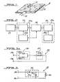
- the invention operates to protect against accidental shock or electrocution in a device like that shown in Fig. 1.
- the general operation of the invention may be understood from Fig. 2.
- Fig. 1 shows a prior art device in which exposed conductor 10 is divided into a series of conductive strips 12 of alternating polarity.
- the arrangement of contacts on vehicle 14 is such that current is conducted through the motor in all positions of vehicle 14 on conductor 10.
- an exposed conductor shaped as a surface, rail or track, provides power through contacts to an electrical device of some sort.
- a part of a human body such as hand 16 to come in contact with conductor 10 in such a way as to receive an electrical current. This may happen accidentally or because a person does not realize that the conductor 10 is energized. In addition, if the device is a toy for children, contact with conductor 10 may result from the user's failure to understand the risk of shock or electrocution.
- protection circuit 24 The power from power source 22 is provided to conductor 26 through protection circuit 24.
- the power may be either direct current CDC) or alternating current (AC), and the term "power" is used herein to cover both DC and AC power.
- power control circuit 24a within protection circuit 24 normally operates to permit power to flow to conductor 26 but periodically interrupts the flow of power.
- sensing circuit 24b monitors conductor 26 to sense whether an object such as a part of a human body is contacting conductor 26.
- Sensing circuit 24b may passively monitor an electrical characteristic such as capacitance or may actively monitor by supplying a signal, such as a medium or high frequency signal of low amplitude, and measuring changes in the signal. If sensing circuit 24b detects : no object, power control circuit 24a continues with normal operation, restoring the flow of power after the interruption. If, on the other hand, sensing circuit 24b detects an object contacting conductor 26, it provides a contact signal to power control circuit 24a. Power control circuit 24a then maintains the interruption of the flow of power, protecting against the risk that current will be conducted through the part of the body from conductor 26.
- a signal such as a medium or high frequency signal of low amplitude
- Fig. 2 also shows contacting device 28 for receiving power from conductor 26.
- Contacting device 28 includes barrier circuit 28a, a circuit which ordinarily permits power to flow freely to load 28b.
- barrier circuit 28a changes to a different electrical state, such as a high impedance state, in which sensing circuit 24b is able to detect contact with an object such as a part of a body even though contacting device 28 remains in contact with conductor 26.
- sensing circuit 24b is able to distinguish between contact with barrier circuit 28a and contact with a part of a body.
- Fig. 2 provide a protection device for electrical apparatus according to the invention and also operate to perform the method of the invention.
- Figs. 3 and 4 show in greater detail the electrical circuitry of the invention and
- Figs. 5A, 5B and 6 show in greater detail the wave forms resulting from operation of the invention.
- FIGs. 3 and 3A show specific electrical circuits which may be used in the contacting device 28 which receives power from conductor 26.
- Fig. 4 shows a specific example of a protection circuit 24 which may be used in the invention.
- sensing circuit 24b could be designed to sense the difference between the state of conductor 26 with no object contacting it and its state when contacted by a part of the human body, sensing circuit 24b must also distinguish between contact with a human body and contact with contacting device 28.
- circuit 30, as shown in Fig. 3 provides electrical characteristics for contacting device 28 which are distinguishable from the electrical characteristics of a part of the human body.
- Circuit 30 includes barrier circuit 32 connected to load 34.
- load 34 will be a motor which receives power through nodes 36 and 38.
- Nodes 36 and 38 may be contacts which rest directly on conductor 26, or they may be the output of a circuit which receives power from two or more contacts and provides that power to nodes 36 and 38.
- Barrier circuit 32 includes capacitor 32b connected in parallel across load 34 and diode 32a connected in series with the parallel circuit.
- diode 32a When a voltage is applied across nodes 36 and 38, diode 32a will become conductive, so that load 34 will draw power and capacitor 32b will charge to the applied voltage less the voltage drop across diode 32a. Then, when the applied voltage is interrupted, diode 32a will immediately be reverse biased and will be non-conductive, because of the voltage on capacitor 32b, so that the current through diode 32a will be interrupted. Capacitor 32b will then discharge through load 34, supplying power to the load while maintaining the proper voltage level across the load during the brief interruption.
- the electrical characteristics of circuit 30, as seen across nodes 36 and 38, will be those of the high impedance state of diode 32a.
- diode 32a may be a low capacitance diode, of approximately 5-50 picofarads in its high impedence state.
- a part of the human body will typically have a capacitance of about 200 picofarads, so that a part of the human body may be readily distinguished from contacting device 28.
- diode 32a must be capable of withstanding a reverse voltage nearly as great as the voltage applied, at least for a brief time.
- Fig. 3A shows alternative circuit 130 which may be used to provide electrical characteristics for contacting device 28 where an alternating current (AC) is applied across nodes 136 and 138.
- Barrier circuit 132 includes two anti-parallel diodes 132a and 132b. When power is applied in either direction across nodes 136 and 138 at a level greater than the barrier voltage of diodes 132a and 132b, one of the diodes will be in a low impedence state and will permit current to flow freely through load 134. Therefore, circuit 130 can be used where an AC current is applied across nodes 136 and 138.
- diodes 132a and 132b will both be in a relatively non-conductive high impedence state. Under these conditions, the current through load 134 is immediately interrupted when power control circuit 24a interrupts the flow of power to conductor 26.
- Circuits 30 and 130 use diodes 32a, 132a and 132b as voltage sensitive devices which allow a useful current to be drawn above a certain voltage, called the barrier voltage, but which prevent current flow below the barrier voltage.
- Diodes 32a, 132a and 132b may thus be ordinary diodes. Instead of a diode, however, a transistor switching circuit or other appropriate switching circuit could be used. :
- Oscillator 40 is constructed around NOR gates 42a and 42b. These gates, together with other NOR gates discussed below, may be parts of a standard 4001 integrated circuit (IC).
- resistors 44 and 46 and capacitor 48 may be provided with appropriate values.
- resistor 44 may be 33 K ohms
- resistor 46 may be 1 megohm
- capacitor 48 may be 0.1 microfarads.
- the oscillating output from oscillator 40 functions as a clock for D-type flip-flop 52 in switching circuit 50.
- the D input to flip-flop 52 is connected to a stable voltage V 1 , which is a high voltage representing a logical "one".
- the preset (PR) input is connected to ground.
- the Q output of flip-flop 52 is connected through NOR gate 54, which will normally function as an inverter, changing the sign of a series of pulses from flip-flop 52, as discussed in relation to Figs. 5A and 5B, below.
- the pulses from NOR gate 54 are then provided through resistor 60 to an arrangement of transistors for controlling the actual flow of power from the power source.
- the power received from the power source is at voltage V 2 , which may be +28 volts.
- Switching transistor 62 operates through resistor 64 to maintain power transistor 68 in a conductive condition.
- switching transistor 62 is rendered non-conductive, and acts with resistor 66 to turn off power transistor 68, interrupting the flow of power to conductor 26.
- resistor 60 may be 10 K ohms and resistors 64 and 66 may each be 4.7 K ohms.
- Switching transistor 62 may be a standard 2N3904 NPN transistor, while power transistor 68 may be a standard IRF-9531 P-channel power MOSFET.
- Power levels V 1 may be provided by a standard 7815 IC, providing 15 volts, for example. In general, V 1 could be any voltage from 5-15 volts representing a logical "one".
- Power level V 2 is supplied by an external power supply.
- the Q output from flip-flop 52 is also conducted through resistor 58 to the clear (CLR) terminal of flip-flop 52.
- the CLR terminal is grounded through capacitor 56.
- This arrangement causes flip-flop 52 to be reset a short time after it is set by a pulse from oscillator 40.
- flip-flop 52 is functioning as a monostable multivibrator. The resulting wave form will be discussed in relation to Fig. 5A below.
- Resistor 58 may be 33 K ohms and capacitor 56 may be 100 picofarads.
- Detection circuit 70 is centered around comparator 72, which functions to compare the voltage level received from conducter 26 with a reference voltage level.
- the reference voltage level is proportioned from voltage V 1 by resistors 74 and 76.
- comparator 72 When the flow of power to conductor 26 is interrupted, the voltage at the "+" terminal of comparator 72 will drop, and when it crosses the reference voltage, comparator 72 will begin to provide a comparison signal to D-type flip-flop 82, which tests the timing of the comparison signal, as described below.
- the D-type flip-flop 82 may, for example, be part of the same 4013 IC as D-type flip-flop 52.
- Comparator 72 may be a standard LM311 device, which will ordinarily pull its output to a low level. Resistor 74 may be 22 K ohms and resistor 76 may be 1 K ohm. In order to pull the signal received by the D input of flip-flop 82 to a high level, when comparator 72 detects equality, voltage V 1 is connected through resistor 84, which may be 33 K ohms. Comparator 72 will permit its output to rise when it begins to provide the comparison signal. When the flow of power to conductor 26 resumes, and the voltage level again crosses the reference voltage level, comparator 72 will stop providing the comparison signal. It will then pull its output down again.
- flip-flop 82 is clocked by the Q output of flip-flop 52, which may be appropriately timed by delay 88. In other words, whenever flip-flop 52 is reset, flip-flop 82 will be clocked so that the output from comparator 72 will be stored. If the voltage level from conducter 26 has dropped below the reference voltage, comparator 72 will permit the D input to flip-flop 82 to be drawn up, beginning the comparison signal. If this occurs before flip-flop 82 is clocked, the subsequent clocking of flip-flop 82 will cause it to store a high value, so that the Q output will remain low. When, however, the comparison signal does not go high until after flip-flop 82 is clocked, the Q output goes high. This causes NOR gate 54 to have a low output regardless of the Q output from flip-flop 52. As a result, the interruption of power is maintained regardless of the sequence of pulses from flip-flop 52.
- Reset circuit 90 includes push-button switch 92 or other appropriate switch for connecting to voltage V i , which represents a logical "one".
- V i represents a logical "one".
- the PR input to flip-flop 82 will be grounded through resistor 94, which may be 33 K ohms.
- switch 92 is closed, however, the PR input to flip-flop 82 will go high, causing the contact signal to return to a low value. This permits the normal operation of the switching circuit 50 to resume, and power will be restored to conductor 26.
- the input from reset circuit 90 is also connected to NOR gate 86, which ensures that flip-flop 82 will be prevented from being cleared after it is preset by the signal from reset circuit 90.
- flip-flop 82 During those periods in which the contact signal is low, indicating that no object has been detected, the Q output of flip-flop 82 remains high, which also operates through NOR gate 86 to prevent the clearing or resetting of flip-flop 82. As a result of this arrangement, flip-flop 82 will be stable in either state.
- protection circuit 24 may be automatically reset after an interruption has continued for some predetermined period.
- a counter could be connected to begin receiving the output of oscillator 40 at the beginning of the contact signal, with its overflow connected to the PR input of flip-flop 82.
- power would be restored after a time period determined by the size of the counter, which would provide a resetting input signal at its overflow value.
- pulses of less than one second duration at ordinary current levels may be perceptible but are generally not sufficient to cause involuntary muscle contraction.
- Each pulse in the protection circuit 24 of Fig. 4 will typically be much shorter than 1 second, and only one pulse would be necessary to test for the contacting object after a period of interruption. Such a pulse would not have a harmful effect.
- the electrical circuit of Fig. 4 is capable of detecting a difference in the rate at which the voltage on conductor 26 drops when the flow of power is interrupted. Therefore, protection circuit 24, as shown in Fig. 4, will be useful for detecting a difference in capacitance. Many other similar circuits could be provided for the same purpose, however, and other parameters could also be used to detect an object contacting the exposed conductor, such as leakage current out of or into the conductor 26 or the effect of a body on a small medium or high frequency signal applied to conductor 26 during the interruption of power. In addition, circuit 24 could be readily modified or another circuit could be provided for use with an AC current.
- FIG. 5A, 5B and 6 Each of these figures is a timing diagram showing pulse characteristics within the electrical circuitry of Fig. 4.
- Fig. 5A illustrates the pulse sequence from the Q output of flip-flop 52.
- the basic features of this sequence are that a series of relatively narrow, rectangu- ler pulses are separated by relatively long periods of a low signal.
- the length of each of the pulses is exaggerated in Fig. 5A, so that each pulse is actually much shorter in relation to the time between pulses than shown.
- each pulse may be approximately 1 microsecond in length, and there may be as many as 500 pulses per second.
- Fig. 5B shows the voltage level on conductor 26.
- this wave form consists of relatively long periods of constant voltage V 2 .
- This voltage is periodically interrupted briefly by a pulse such as pulses 102a and 102b, each of which has the same length as each pulse 100a in Fig. 5A.
- NOR gate 54 simply inverts the Q output of flip-flop 5 : 2 and the voltage tq conductor 26 corresponds to the inverted signal from NOR gate 54.
- the contact signal goes high, and NOR gate 54 is locked with a low output.
- Fig. 6 shows in detail the characteristics of pulse 102, which represents one of the pulses in the voltage on conductor 26.
- Pulse 102 immediately drops the voltage to barrier voltage 114, which is the voltage at which barrier circuit 28a enters its high impedence state.
- barrier voltage 114 is the voltage at which barrier circuit 28a enters its high impedence state.
- diode 32a will then begin to act as a capacitor, discharging along curve 110 if no body is contacting conductor 26.
- Reference voltage 116 which is less than barrier voltage 114 but greater than curve 110 at time 118, will be compared with the voltage on conductor 26 by detection circuit 70, which will then provide a comparison signal. This will occur before flip-flop 82 is clocked at time 118, so that the contact signal will remain low.
- the electrical circuitry shown in Fig. 4 is appropriate for distinguishing between the capacitance of a part of a body and that of the contacting device 28. If. on the other hand, the leakage current were being used to distinguish, diodes 32a, 132a and 132b should be low leakage diodes, so that all leakage would be through the part of the body rather than through the diodes. In this case. an electrical circuit designed to detect variations in the leakage current during the interruption of the flow of power would be used.
Landscapes
- Emergency Protection Circuit Devices (AREA)
Applications Claiming Priority (2)
| Application Number | Priority Date | Filing Date | Title |
|---|---|---|---|
| US656431 | 1984-10-01 | ||
| US06/656,431 US4630161A (en) | 1984-10-01 | 1984-10-01 | Protection technique for exposed conductor |
Publications (3)
| Publication Number | Publication Date |
|---|---|
| EP0177305A2 true EP0177305A2 (fr) | 1986-04-09 |
| EP0177305A3 EP0177305A3 (en) | 1987-09-23 |
| EP0177305B1 EP0177305B1 (fr) | 1990-04-11 |
Family
ID=24633001
Family Applications (1)
| Application Number | Title | Priority Date | Filing Date |
|---|---|---|---|
| EP85306914A Expired - Lifetime EP0177305B1 (fr) | 1984-10-01 | 1985-09-27 | Technique de protection pour un conducteur accessible |
Country Status (6)
| Country | Link |
|---|---|
| US (1) | US4630161A (fr) |
| EP (1) | EP0177305B1 (fr) |
| JP (1) | JPS61180515A (fr) |
| CA (1) | CA1266882A (fr) |
| DE (1) | DE3577165D1 (fr) |
| IL (1) | IL76548A (fr) |
Cited By (1)
| Publication number | Priority date | Publication date | Assignee | Title |
|---|---|---|---|---|
| US5166852A (en) * | 1989-10-31 | 1992-11-24 | Kabushiki Kaisha Toshiba | Electronic circuit device for protecting electronic circuits from unwanted removal of ground terminal |
Families Citing this family (4)
| Publication number | Priority date | Publication date | Assignee | Title |
|---|---|---|---|---|
| JP2746894B2 (ja) * | 1988-01-22 | 1998-05-06 | 株式会社東芝 | 電子機器の電源供給ライン |
| GB2222039B (en) * | 1988-05-23 | 1992-07-01 | B & R Electrical Prod Ltd | Electrical safety apparatus |
| US6724589B1 (en) * | 1999-09-13 | 2004-04-20 | Donald G. Funderburk | Boat electrical test and isolator system |
| WO2017192106A1 (fr) | 2016-05-03 | 2017-11-09 | Guvenli Elektrik Elektronik Sanayi Ticaret Ve Pazarlama Limited Sirketi | Système de commande intelligent destiné à détecter un branchement ou un retrait de dispositifs électriques, à détecter un court-circuit, à détecter un contact humain avec le conducteur et à protéger un être humain contre des chocs électriques |
Citations (6)
| Publication number | Priority date | Publication date | Assignee | Title |
|---|---|---|---|---|
| GB1035328A (en) * | 1963-11-21 | 1966-07-06 | Wallacetown Engineering Compan | Earth leakage protective device |
| US3465475A (en) * | 1965-10-21 | 1969-09-09 | Lewis Arnow | Electrically operable toy vehicle and electrified surface |
| US3784842A (en) * | 1972-02-03 | 1974-01-08 | F Kremer | Body current activated circuit breaker |
| DE2357081A1 (de) * | 1973-11-15 | 1975-05-28 | Gerd Dr Ing Harms | Verfahren und einrichtung zur messung des isolationswiderstandes von ungeerdeten gleichstromnetzen |
| US3997818A (en) * | 1973-07-05 | 1976-12-14 | Bodkin Lawrence E | Load selective power systems |
| US4029996A (en) * | 1976-03-08 | 1977-06-14 | The Gillette Company | Apparatus having a protective circuit |
Family Cites Families (3)
| Publication number | Priority date | Publication date | Assignee | Title |
|---|---|---|---|---|
| DE2145538C3 (de) * | 1971-09-08 | 1975-01-23 | Loewe Opta Gmbh, 1000 Berlin | Elektronische Sicherungsanordnung |
| US4175255A (en) * | 1977-09-06 | 1979-11-20 | Branderud Nils P | Device to protect against flow of current |
| DE3216497A1 (de) * | 1982-05-03 | 1983-11-03 | Siemens AG, 1000 Berlin und 8000 München | Vorrichtung zur inbetriebnahme der fernspeisung von elektrischen verbrauchern und schaltungsanordnung zur durchfuehrung des verfahrens |
-
1984
- 1984-10-01 US US06/656,431 patent/US4630161A/en not_active Expired - Fee Related
-
1985
- 1985-09-27 DE DE8585306914T patent/DE3577165D1/de not_active Expired - Fee Related
- 1985-09-27 EP EP85306914A patent/EP0177305B1/fr not_active Expired - Lifetime
- 1985-10-01 JP JP60218987A patent/JPS61180515A/ja active Pending
- 1985-10-01 CA CA000491982A patent/CA1266882A/fr not_active Expired - Fee Related
- 1985-10-02 IL IL76548A patent/IL76548A/xx unknown
Patent Citations (6)
| Publication number | Priority date | Publication date | Assignee | Title |
|---|---|---|---|---|
| GB1035328A (en) * | 1963-11-21 | 1966-07-06 | Wallacetown Engineering Compan | Earth leakage protective device |
| US3465475A (en) * | 1965-10-21 | 1969-09-09 | Lewis Arnow | Electrically operable toy vehicle and electrified surface |
| US3784842A (en) * | 1972-02-03 | 1974-01-08 | F Kremer | Body current activated circuit breaker |
| US3997818A (en) * | 1973-07-05 | 1976-12-14 | Bodkin Lawrence E | Load selective power systems |
| DE2357081A1 (de) * | 1973-11-15 | 1975-05-28 | Gerd Dr Ing Harms | Verfahren und einrichtung zur messung des isolationswiderstandes von ungeerdeten gleichstromnetzen |
| US4029996A (en) * | 1976-03-08 | 1977-06-14 | The Gillette Company | Apparatus having a protective circuit |
Cited By (1)
| Publication number | Priority date | Publication date | Assignee | Title |
|---|---|---|---|---|
| US5166852A (en) * | 1989-10-31 | 1992-11-24 | Kabushiki Kaisha Toshiba | Electronic circuit device for protecting electronic circuits from unwanted removal of ground terminal |
Also Published As
| Publication number | Publication date |
|---|---|
| EP0177305B1 (fr) | 1990-04-11 |
| JPS61180515A (ja) | 1986-08-13 |
| CA1266882A (fr) | 1990-03-20 |
| EP0177305A3 (en) | 1987-09-23 |
| DE3577165D1 (de) | 1990-05-17 |
| IL76548A (en) | 1989-10-31 |
| IL76548A0 (en) | 1986-04-29 |
| US4630161A (en) | 1986-12-16 |
Similar Documents
| Publication | Publication Date | Title |
|---|---|---|
| US5563799A (en) | Low cost/low current watchdog circuit for microprocessor | |
| US5142432A (en) | Fault detection apparatus for a transformer isolated transistor drive circuit for a power device | |
| CA1067581A (fr) | Detecteur de baisse de courant | |
| US4245150A (en) | Power line disturbance detector circuit | |
| US4429236A (en) | Apparatus for generating pulses upon decreases in supply voltage | |
| AU661361B2 (en) | Fail-safe condition sensing circuit for the detection of flame | |
| EP0605997A1 (fr) | Méthode et dispositif pour détecter une résistance de fuite dans un véhicule électrique | |
| US3891895A (en) | Ground fault detection | |
| JPS5985521A (ja) | 低電圧負荷用位相制御回路 | |
| US4485342A (en) | Load driving circuitry with load current sensing | |
| EP0177305B1 (fr) | Technique de protection pour un conducteur accessible | |
| US5138547A (en) | Dual input power supply | |
| US4115731A (en) | System for locating electrical shorts by tracking the paths of injected pulse currents utilizing a voltage differential responsive probe | |
| EP0102659B1 (fr) | Circuit de contrôle de la vitesse du moteur d'une machine à laver | |
| JPH0659779A (ja) | 電圧遷移を検出する方法 | |
| EP0301084B1 (fr) | Appareil et procede de controle d'interruptions de contact dans des dispositifs d'interconnexion de circuits. | |
| JPS62188420A (ja) | 交流無接点スイツチ | |
| JP2002084173A (ja) | 電力用半導体装置及び過電流保護回路 | |
| US4328527A (en) | Selective ultraviolet signal amplifier circuit | |
| AU656838B2 (en) | Circuit for detecting firing of an ultraviolet radiation detector tube | |
| JP2552042B2 (ja) | Scrの導電測定方法及び測定装置 | |
| US6310557B1 (en) | Circuit and device to detect grounding problems in electrical soldering irons | |
| US5126659A (en) | Enablement of a test mode in an electronic module with limited pin-outs | |
| KR0179869B1 (ko) | 전자접촉기의 제어장치 | |
| JPH0335170A (ja) | 交流電源停電検出回路 |
Legal Events
| Date | Code | Title | Description |
|---|---|---|---|
| PUAI | Public reference made under article 153(3) epc to a published international application that has entered the european phase |
Free format text: ORIGINAL CODE: 0009012 |
|
| AK | Designated contracting states |
Kind code of ref document: A2 Designated state(s): DE FR GB IT |
|
| PUAL | Search report despatched |
Free format text: ORIGINAL CODE: 0009013 |
|
| AK | Designated contracting states |
Kind code of ref document: A3 Designated state(s): DE FR GB IT |
|
| 17P | Request for examination filed |
Effective date: 19880225 |
|
| 17Q | First examination report despatched |
Effective date: 19880614 |
|
| GRAA | (expected) grant |
Free format text: ORIGINAL CODE: 0009210 |
|
| AK | Designated contracting states |
Kind code of ref document: B1 Designated state(s): DE FR GB IT |
|
| ITF | It: translation for a ep patent filed |
Owner name: ING. C. GREGORJ S.P.A. |
|
| REF | Corresponds to: |
Ref document number: 3577165 Country of ref document: DE Date of ref document: 19900517 |
|
| ET | Fr: translation filed | ||
| PLBE | No opposition filed within time limit |
Free format text: ORIGINAL CODE: 0009261 |
|
| STAA | Information on the status of an ep patent application or granted ep patent |
Free format text: STATUS: NO OPPOSITION FILED WITHIN TIME LIMIT |
|
| 26N | No opposition filed | ||
| PGFP | Annual fee paid to national office [announced via postgrant information from national office to epo] |
Ref country code: GB Payment date: 19910913 Year of fee payment: 7 |
|
| PGFP | Annual fee paid to national office [announced via postgrant information from national office to epo] |
Ref country code: FR Payment date: 19910916 Year of fee payment: 7 |
|
| PGFP | Annual fee paid to national office [announced via postgrant information from national office to epo] |
Ref country code: DE Payment date: 19910924 Year of fee payment: 7 |
|
| ITTA | It: last paid annual fee | ||
| PG25 | Lapsed in a contracting state [announced via postgrant information from national office to epo] |
Ref country code: GB Effective date: 19920927 |
|
| GBPC | Gb: european patent ceased through non-payment of renewal fee |
Effective date: 19920927 |
|
| PG25 | Lapsed in a contracting state [announced via postgrant information from national office to epo] |
Ref country code: FR Effective date: 19930528 |
|
| PG25 | Lapsed in a contracting state [announced via postgrant information from national office to epo] |
Ref country code: DE Effective date: 19930602 |
|
| REG | Reference to a national code |
Ref country code: FR Ref legal event code: ST |