EP0176818B1 - Temperature-compensated oscillation device - Google Patents
Temperature-compensated oscillation device Download PDFInfo
- Publication number
- EP0176818B1 EP0176818B1 EP85111409A EP85111409A EP0176818B1 EP 0176818 B1 EP0176818 B1 EP 0176818B1 EP 85111409 A EP85111409 A EP 85111409A EP 85111409 A EP85111409 A EP 85111409A EP 0176818 B1 EP0176818 B1 EP 0176818B1
- Authority
- EP
- European Patent Office
- Prior art keywords
- signal
- digital
- temperature
- digital signal
- frequency
- Prior art date
- Legal status (The legal status is an assumption and is not a legal conclusion. Google has not performed a legal analysis and makes no representation as to the accuracy of the status listed.)
- Expired
Links
Images

Classifications
-
- H—ELECTRICITY
- H03—ELECTRONIC CIRCUITRY
- H03L—AUTOMATIC CONTROL, STARTING, SYNCHRONISATION, OR STABILISATION OF GENERATORS OF ELECTRONIC OSCILLATIONS OR PULSES
- H03L1/00—Stabilisation of generator output against variations of physical values, e.g. power supply
- H03L1/02—Stabilisation of generator output against variations of physical values, e.g. power supply against variations of temperature only
- H03L1/022—Stabilisation of generator output against variations of physical values, e.g. power supply against variations of temperature only by indirect stabilisation, i.e. by generating an electrical correction signal which is a function of the temperature
- H03L1/023—Stabilisation of generator output against variations of physical values, e.g. power supply against variations of temperature only by indirect stabilisation, i.e. by generating an electrical correction signal which is a function of the temperature by using voltage variable capacitance diodes
- H03L1/025—Stabilisation of generator output against variations of physical values, e.g. power supply against variations of temperature only by indirect stabilisation, i.e. by generating an electrical correction signal which is a function of the temperature by using voltage variable capacitance diodes and a memory for digitally storing correction values
Definitions
- the present invention relates to a temperature-compensated oscillation device and, more particularly, to a digitally controlled temperature-compensated oscillation device.
- a digitally controlled temperature-compensated oscillation device has been extensively used as a local oscillator of a mobile radio apparatus because its frequency generally remains stable over a wide temperature range.
- Such a type of oscillation device comprises a temperature sensing section made up of a temperature sensor and an analog-to-digital (A/D) converter, a read only memory (ROM) which stores compensation data associated with outputs of the A/D converter, and an oscillating section responsive to an output of the ROM and made up of a digital-to-analog (D/A) converter and a voltage controlled oscillator (VCO).
- A/D analog-to-digital
- ROM read only memory
- VCO voltage controlled oscillator
- the problem with an oscillation device having the above construction is that a noticeable variation in ambient temperature causes an output of the A/D converter, i.e., an output value of the ROM, to sharply vary for a moment to thereby add frequency modulation noise and phase modulation noise to an output of the VCO.
- Such, in a multichannel communication system constitutes a source of noise for other channels or needs to be coped with by designing the exclusive frequency band undesirably wide .
- DE-A- 29 36 378 discloses a device for compensating the frequency/temperature relation of a crystal oscillator in an oscillator circuit.
- the device is provided with a capacitance diode which fine-tunes the frequency of the crystal oscillator in dependence of the voltage applied to said diode.
- the fine tuning voltage does not change continuously in dependence of the temperature. but abruptly in predetermined temperature intervals.
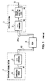
- the device comprises a temperature sensing section 1 made up of a temperature sensor 11 and an analog-to-digital (A/D) converter 12, a read only memory (ROM) 21, and an oscillating section 3 made up of a digital-to-analog (D/A) converter 31 and a voltage-controlled oscillator (VCO) 32.
- the VCO 32 comprises a crystal oscillator and a variable capacitance element.
- the temperature sensor 11 senses an ambient temperature to convert it to a voltage which is applied as a temperature data signal 101 to the A/D converter 12.
- the A/D converter 12 quantizes the input signal 101 to provide a first digital value which is produced as a first digital signal 102.
- This signal 102 is delivered to an address input terminal of the ROM 21 so as to specify a particular address of the latter, whereby a second digital value stored in that address is outputted as a second digital signal 205a.
- the D/A converter 31 to which the second digital signal 205a is routed transforms the signal 205a into a voltage and applies the voltage as a frequency control signal 301 to the VCO 32. Responsive to the signal 301, the VCO 32 controls the capacitance of its variable capacitance element and, as a result, temperature-compensates the frequency of an oscillation signal 302, which is an output of the VCO 32.
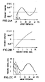
- the frequency of the oscillation signal 302 may vary with the ambient temperature as shown in Fig. 2A.
- the graph represents a relationship between the temperature surrounding the crystal oscillator of the VCO 32 and the variation of its resonance frequency.
- the frequency of the oscillation signal 302 may vary with the frequency control signal 301 as shown in Fig. 2B. If the relationship between the first digital signal 102 and the second digital signal 205a in the ROM 21 is selected such that the relationship shown in Fig.
- the frequency of the oscillation signal 302 will be temperature-compensated.
- the curve shown in Fig. 2C is stepwise because the ambient temperature is quantized as the first digital signal 102.
- the frequency variation of the oscillation signal 302 after temperature compensation is shown in Fig. 3 relative to the ambient temperature. Comparing Fig. 3 with Fig. 2A, it will be seen that as a result of temperature compensation the frequency variation of the oscillation signal 302 has been reduced to about 1/4 over the temperature range of -20°C to +60°C.
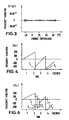
- the ambient temperature as shown in Fig. 4 is assumed to increase with time and a temperature T1 is associated with a time t1 and a temperature T2 with a time t2.
- the frequency control signal 301 remains at a constant voltage V1 and the frequency of the oscillation signal 302 increases with time.
- the signal 301 shifts from the voltage V1 to a voltage V2 and, at this moment, the frequency of the signal 302 is sharply lowered. In this manner, at the moment when the output of the A/D converter is varied, the frequency of the oscillation signal 302 is sharply varied with the result that frequency modulation noise and phase modulation noise are added to the signal 302.
- the digitally temperature-controlled oscillation device installed in a radio frequency or phase modulation communication system is sufficiently small in frequency variation, but cannot avoid a substantial magnitude of noise as previously discussed.
- the influence of noise extends even to other channels.
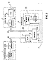
- the oscillation device comprises a temperature sensing section 1 which includes a temperature sensor 11 and an A/D converter 12, a control section 2 made up a ROM 21, a comparator 22 and an up-down counter 23, and an oscillating section 3 made up of a D/A converter 31 and a VCO 32.
- the VCO 32 comprises a crystal oscillator and a variable capacitance element.
- the temperature sensor 11 converts an ambient temperature to a voltage and produces the voltage as a temperature data signal 101.
- the A/D converter 12 quantizes it to provide a first digital value and applies the first digital value as a first digital signal 102 to an address input terminal of the ROM 21.
- the ROM 21 produces a third digital value (assumed to have a value A) from a particular address thereof which is specified by the input signal 102, the third digital value being applied to one input terminal of the comparator 22.
- Applied to the other input terminal of the comparator 22 is a count from the up-down counter 23 (assumed to have a value B).
- the comparator 22 also produces a discrimination signal 203 which is a high level "1" when A > B and a low level "0" when A ⁇ B.
- the identification signal 202 and the discrimination signal 203 are applied to the up-down counter 23.
- a clock signal 204 is also applied to the up-down counter 23 via a clock input terminal 24 of the control section 2. While the identification signal 202 is a high level, the counter 23 is disenabled to maintain the value B equal to the value A. While the identification signal 202 is a low level and the discrimination signal 203 is a high level, the counter 23 is incremented responsive to each pulse of the clock signal 204.
- the output 205 of the counter 23 is also applied to the D/A converter 31.
- the D/A converter 31 converts the input signal 205 to a voltage and applies it to the VCO 301 as a frequency control signal 301.
- the signal 301 controls the capacitance of the variable capacitance element of the VCO 301 to thereby temperature-compensate the frequency of an oscillation signal 302 which is outputted from the oscillation device.
- control section 2 converts a variation in the first digital signal 102 to a plurality of time-divided fractional variations in the output 205 of the counter 23.
- FIG. 6 an exemplary relationship between time and the frequency variation of the oscillation signal 302 in accordance with the illustrative embodiment is shown, the temperature being assumed as varying with time.
- a value A associated with an ambient temperature at a time immediately before a time t1 is A1
- the value A1 has changed to A2 at the time t1.
- the value B changes from A1 to (A1 - 1) at the time t1, to (A1 - 2) at a time (t1 + t c ), and to (A1 - 3) at a time (t1 + 2t c ), where t c is the period of the clock signal 204.
- t c is the period of the clock signal 204.
- A2 is equal to (A1 - 3).
- the frequency of the oscillation signal 302 is also varied in a stepwise manner at those times. Comparing Fig. 6 with Fig. 4, it will be apparent that the stepwise variations, i.e., the amounts of sharp variations of the frequency of the signal 302 are smaller in the illustrative embodiment than in the prior art and, as a result, noise introduced into the signal 302 due to the sharp frequency variations is reduced.
- FIG. 7 another embodiment of the present invention is shown.
- the oscillation device in this particular embodiment differs from that of Fig. 5 in that the up-down counter 23 of the latter is replaced with a gate 25 and an up-down counter 26, and in that the identification signal 202 and clock signal 204 are applied to the gate 25.
- the gate 25 is enabled to pass the clock signal 204 to the up-down counter 26 as an output signal 206.
- the gate 25 is disenabled to interrupt the supply of the clock signal 204 to the counter 26.
- the gate 25 and the counter 26 cooperates, as labeled 23a in the drawing, to fulfill the function which is assigned to the counter 23 of the first embodiment.
- the embodiment of Fig. 7 is the same in operation and effect as the embodiment of Fig. 5.
- the present invention provides a temperature-compensated oscillation device which reduces frequency variations and noise over a wide temperature range.
- a radio communication apparatus implemented with such a device of the present invention will narrow the exclusive frequency band width, compared to a prior art apparatus.
- ROM 21 is used in the illustrative embodiments to serve the function of numerical value conversion means for converting the first digital signal 102 to the third digital signal 201, such a function may alternatively be fulfilled by means of a memory which generates a constant of a polynominal for converting a first digital value to a second digital value and an operation unit for operating the polynomial.
- a kind of conversion means is disclosed in JP-A-58-184809, for example.
- the crystal oscillator included in the VCO 32 may be replaced with an elastic surface wave element.
- the clock signal input terminal 24 may be omitted and, instead, a clock signal generator may be added to the control section 2, in which case the output of the clock signal generator will serve as the clock signal 204.
Description
- The present invention relates to a temperature-compensated oscillation device and, more particularly, to a digitally controlled temperature-compensated oscillation device.
- A digitally controlled temperature-compensated oscillation device has been extensively used as a local oscillator of a mobile radio apparatus because its frequency generally remains stable over a wide temperature range. Such a type of oscillation device comprises a temperature sensing section made up of a temperature sensor and an analog-to-digital (A/D) converter, a read only memory (ROM) which stores compensation data associated with outputs of the A/D converter, and an oscillating section responsive to an output of the ROM and made up of a digital-to-analog (D/A) converter and a voltage controlled oscillator (VCO).
- The problem with an oscillation device having the above construction is that a noticeable variation in ambient temperature causes an output of the A/D converter, i.e., an output value of the ROM, to sharply vary for a moment to thereby add frequency modulation noise and phase modulation noise to an output of the VCO. Such, in a multichannel communication system, constitutes a source of noise for other channels or needs to be coped with by designing the exclusive frequency band undesirably wide .
- DE-A- 29 36 378 discloses a device for compensating the frequency/temperature relation of a crystal oscillator in an oscillator circuit. The device is provided with a capacitance diode which fine-tunes the frequency of the crystal oscillator in dependence of the voltage applied to said diode. The fine tuning voltage does not change continuously in dependence of the temperature. but abruptly in predetermined temperature intervals.
- It is an object of the present invention to provide a digitally controlled temperature-compensated oscillation device which reduces the previously mentioned kinds of noise.
- This object is achieved by the oscillator device according to the claims.
- The above and other objects, features and advantages of the present invention will become more apparent from the following detailed description taken with the accompanying drawings in which:
- Fig. 1 is a block diagram of a prior art temperature-compensated oscillation device;
- Figs. 2A - 2C are graphs representative of the operation of a voltage-controlled oscillator applicable to the present invention as well as to the prior art, specifically Fig. 2A showing an oscillation signal frequency variation against ambient temperature characteristic, Fig. 2B an oscillation signal frequency variation against frequency control signal characteristic, and Fig. 2C a frequency control signal against ambient temperature characteristic;
- Fig. 3 is a graph showing an oscillation signal frequency variation against ambient temperature characteristic of a prior art temperature-compensated oscillation device and that of the present invention;
- Fig. 4 is a graph showing an oscillation signal frequency variation against time characteristic of the prior art temperature-compensated oscillation device;
- Fig. 5 is a block diagram of a temperature-compensated oscillation device embodying the present invention;
- Fig. 6 is an oscillation signal frequency variation against time characteristic particular to the temperature-compensated oscillation device of the present invention; and
- Fig. 7 is a block diagram showing another embodiment of the present invention.
- To better understand the present invention, a brief reference will be made to a prior art digitally controlled oscillation device, shown in Fig. 1. As shown, the device comprises a
temperature sensing section 1 made up of atemperature sensor 11 and an analog-to-digital (A/D)converter 12, a read only memory (ROM) 21, and an oscillatingsection 3 made up of a digital-to-analog (D/A)converter 31 and a voltage-controlled oscillator (VCO) 32. TheVCO 32 comprises a crystal oscillator and a variable capacitance element. Thetemperature sensor 11 senses an ambient temperature to convert it to a voltage which is applied as atemperature data signal 101 to the A/D converter 12. The A/D converter 12 quantizes theinput signal 101 to provide a first digital value which is produced as a firstdigital signal 102. Thissignal 102 is delivered to an address input terminal of theROM 21 so as to specify a particular address of the latter, whereby a second digital value stored in that address is outputted as a seconddigital signal 205a. The D/A converter 31 to which the seconddigital signal 205a is routed transforms thesignal 205a into a voltage and applies the voltage as afrequency control signal 301 to theVCO 32. Responsive to thesignal 301, theVCO 32 controls the capacitance of its variable capacitance element and, as a result, temperature-compensates the frequency of anoscillation signal 302, which is an output of theVCO 32. - Details of the temperature compensation effected as above will be described with reference to Figs. 2A - 2C. While the
frequency control signal 301 is maintained at a certaian constant value, the frequency of theoscillation signal 302 may vary with the ambient temperature as shown in Fig. 2A. Specifically, the graph represents a relationship between the temperature surrounding the crystal oscillator of theVCO 32 and the variation of its resonance frequency. Meanwhile, when the ambient temperature remains constant, the frequency of theoscillation signal 302 may vary with thefrequency control signal 301 as shown in Fig. 2B. If the relationship between the firstdigital signal 102 and the seconddigital signal 205a in theROM 21 is selected such that the relationship shown in Fig. 2C holds between the ambient temperature and thefrequency control signal 301, the frequency of theoscillation signal 302 will be temperature-compensated. The curve shown in Fig. 2C is stepwise because the ambient temperature is quantized as the firstdigital signal 102. The frequency variation of theoscillation signal 302 after temperature compensation is shown in Fig. 3 relative to the ambient temperature. Comparing Fig. 3 with Fig. 2A, it will be seen that as a result of temperature compensation the frequency variation of theoscillation signal 302 has been reduced to about 1/4 over the temperature range of -20°C to +60°C. - Referring to Fig. 4, there is shown a graph representative of exemplary frequency variations of the
oscillation signal 302 with respect to time which occur while the ambient temperature is varied with time. As understood by comparing Fig. 4 With Figs. 2A and 2C, the ambient temperature as shown in Fig. 4 is assumed to increase with time and a temperature T₁ is associated with a time t₁ and a temperature T₂ with a time t₂. During the period between the times t₁ and t₂, thefrequency control signal 301 remains at a constant voltage V₁ and the frequency of theoscillation signal 302 increases with time. At the time t₂, thesignal 301 shifts from the voltage V₁ to a voltage V₂ and, at this moment, the frequency of thesignal 302 is sharply lowered. In this manner, at the moment when the output of the A/D converter is varied, the frequency of theoscillation signal 302 is sharply varied with the result that frequency modulation noise and phase modulation noise are added to thesignal 302. - Thus, the digitally temperature-controlled oscillation device installed in a radio frequency or phase modulation communication system is sufficiently small in frequency variation, but cannot avoid a substantial magnitude of noise as previously discussed. In addition, the influence of noise extends even to other channels.
- Referring to Fig. 5, a temperature-compensated oscillation device embodying the present invention is shown which is free from the drawbacks stated above. As shown, the oscillation device comprises a
temperature sensing section 1 which includes atemperature sensor 11 and an A/D converter 12, acontrol section 2 made up aROM 21, acomparator 22 and an up-down counter 23, and an oscillatingsection 3 made up of a D/A converter 31 and aVCO 32. TheVCO 32 comprises a crystal oscillator and a variable capacitance element. Thetemperature sensor 11 converts an ambient temperature to a voltage and produces the voltage as atemperature data signal 101. Responsive to thesignal 101, the A/D converter 12 quantizes it to provide a first digital value and applies the first digital value as a firstdigital signal 102 to an address input terminal of theROM 21. TheROM 21 produces a third digital value (assumed to have a value A) from a particular address thereof which is specified by theinput signal 102, the third digital value being applied to one input terminal of thecomparator 22. Applied to the other input terminal of thecomparator 22 is a count from the up-down counter 23 (assumed to have a value B). Thecomparator 22 produces anidentification signal 202 which is a high level "1" when A = B and a low level "0" when A ≠ B. Thecomparator 22 also produces adiscrimination signal 203 which is a high level "1" when A > B and a low level "0" when A < B. Theidentification signal 202 and thediscrimination signal 203 are applied to the up-downcounter 23. Aclock signal 204 is also applied to the up-downcounter 23 via aclock input terminal 24 of thecontrol section 2. While theidentification signal 202 is a high level, thecounter 23 is disenabled to maintain the value B equal to the value A. While theidentification signal 202 is a low level and thediscrimination signal 203 is a high level, thecounter 23 is incremented responsive to each pulse of theclock signal 204. When theidentification signal 202 is a low level and thediscrimination signal 203 is a high level, thecounter 23 is decremented responsive to each pulse of theclock signal 204. In this manner, thecomparator 22 and thecounter 23 cooperate with each other to maintain the value B equal to the value A when A = B and to increment or decrement the value B to the value A when A ≠ B. Theoutput 205 of thecounter 23 is also applied to the D/A converter 31. The D/A converter 31 converts theinput signal 205 to a voltage and applies it to theVCO 301 as afrequency control signal 301. Thesignal 301 controls the capacitance of the variable capacitance element of theVCO 301 to thereby temperature-compensate the frequency of anoscillation signal 302 which is outputted from the oscillation device. - Thus, the
control section 2 converts a variation in the firstdigital signal 102 to a plurality of time-divided fractional variations in theoutput 205 of thecounter 23. - Referring to Fig. 6, an exemplary relationship between time and the frequency variation of the
oscillation signal 302 in accordance with the illustrative embodiment is shown, the temperature being assumed as varying with time. Assume that a value A associated with an ambient temperature at a time immediately before a time t₁ is A₁, and that the value A₁ has changed to A₂ at the time t₁. Then, the value B changes from A₁ to (A₁ - 1) at the time t₁, to (A₁ - 2) at a time (t₁ + tc), and to (A₁ - 3) at a time (t₁ + 2tc), where tc is the period of theclock signal 204. In the example shown in Fig. 6, A₂ is equal to (A₁ - 3). As the value B is varied at the times t₁, (t₁ + tc) and (t₁ + 2tc), the frequency of theoscillation signal 302 is also varied in a stepwise manner at those times. Comparing Fig. 6 with Fig. 4, it will be apparent that the stepwise variations, i.e., the amounts of sharp variations of the frequency of thesignal 302 are smaller in the illustrative embodiment than in the prior art and, as a result, noise introduced into thesignal 302 due to the sharp frequency variations is reduced. - Referring to Fig. 7, another embodiment of the present invention is shown. The oscillation device in this particular embodiment differs from that of Fig. 5 in that the up-
down counter 23 of the latter is replaced with agate 25 and an up-down counter 26, and in that theidentification signal 202 andclock signal 204 are applied to thegate 25. Specifically, when theidentification signal 202 is a low level, thegate 25 is enabled to pass theclock signal 204 to the up-down counter 26 as anoutput signal 206. When thesignal 202 is a high level, thegate 25 is disenabled to interrupt the supply of theclock signal 204 to thecounter 26. Thegate 25 and thecounter 26 cooperates, as labeled 23a in the drawing, to fulfill the function which is assigned to thecounter 23 of the first embodiment. Hence, the embodiment of Fig. 7 is the same in operation and effect as the embodiment of Fig. 5. - In summary, it will be seen that the present invention provides a temperature-compensated oscillation device which reduces frequency variations and noise over a wide temperature range. Hence, a radio communication apparatus implemented with such a device of the present invention will narrow the exclusive frequency band width, compared to a prior art apparatus.
- Various modifications will become possible for those skilled in the art after receiving the teachings of the present disclosure without departing from the scope thereof. For example, while
ROM 21 is used in the illustrative embodiments to serve the function of numerical value conversion means for converting the firstdigital signal 102 to the thirddigital signal 201, such a function may alternatively be fulfilled by means of a memory which generates a constant of a polynominal for converting a first digital value to a second digital value and an operation unit for operating the polynomial. Such a kind of conversion means is disclosed in JP-A-58-184809, for example. Further, in the illustrative embodiments as well as in the modification mentioned above, the crystal oscillator included in theVCO 32 may be replaced with an elastic surface wave element. In addition, in all the embodiments and their modifications described, the clocksignal input terminal 24 may be omitted and, instead, a clock signal generator may be added to thecontrol section 2, in which case the output of the clock signal generator will serve as theclock signal 204.
Claims (4)
- A temperature-compensated oscillator device comprising:
temperature sensing section means (1) including temperature sensor means (11) for sensing an ambient temperature to provide a temperature data signal (101) representative of the sensed temperature and analog-to-digital converter means (12) for converting the temperature data signal (101) to a first digital signal (102) having a first digital value;
control section means (2) for converting the first digital signal (102) to a second digital signal (205) having a second digital value; and
oscillating section means (3) including converter means (31) for converting the second digital signal (205) to a frequency control signal (301) and voltage-controlled oscillator means (32) responsive to the frequency control signal (301) for changing the oscillation signal frequency thereof;
characterized in that
the control section means (2) comprises first means (21) responsive to the first digital signal (102) for providing a third digital signal (201) corresponding thereto;
second means (22) for comparing the second digital signal (205) with the third digital signal (201) and providing an identification signal (202) indicative of whether the second (205) and third digital signals (201) are coincident with each other and a discrimination signal (203) indicative of which one of the second (205) and third digital signals (201) is greater than the other and
third means (23) responsive to the identification signal (202), the discrimination signal (203) and a clock signal (204) for, when the identification signal (202) indicates coincidence, stopping a count of the clock signal (204) and, when the identification signal (202) indicates non-coincidence, incrementing or decrementing the count in accordance with the discrimination signal (203), thereby providing the second digital signal (205). - A temperature-compensated oscillator device as claimed in Claim 1, wherein the first means (21) comprises a read only memory (21), the second means (22) comprises a digital comparator (22) and the third means (23) comprises an up/down counter (26).
- A temperature-compensated oscillator device comprising:
temperature sensing section means (1) including temperature sensor means (11) or sensing an ambient temperature to provide a temperature data signal (101) representative of the sensed temperature and analog-to-digital converter means (12) for converting the temperature data signal (101) to a first digital signal (102) having a first digital value;
control section means (2) for converting the first digital signal (102) to a second digital signal (205) having a second digital value; and
oscillating section (3) means including converter means (31) for converting the second digital signal (205) to a frequency control signal (301) and voltage-controlled oscillator means (32) responsive to the frequency control signal (301) for changing the oscillation signal frequency thereof;
characterized in that
the control section means (2) comprises first means (21) responsive to the first digital signal (102) for providing a third digital signal (201) corresponding thereto;
second means (22) for comparing the second digital signal (205) with the third digital signal (201) and providing an identification signal (202) indicative of whether the second (205) and third digital signals (201) are coincident with each other and a discrimination signal (203) indicative of which one of the second (205) and third digital signals (201) is greater than the other;
third means (25) for controlling the passing of a clock signal (204) according to the identification signal (202) and
fourth means (26) for counting the output (206) of the third means (25) according to the discrimination signal (203). - A temperature-compensated oscillator device as claimed in Claim 3, wherein the first means (21) comprises a read only memory (21), the second means (22) comprises a digital comparator (22), the third means (25) comprises a gate circuit (25) and the fourth means (26) comprises an up/down counter (26).
Applications Claiming Priority (2)
| Application Number | Priority Date | Filing Date | Title |
|---|---|---|---|
| JP189138/84 | 1984-09-10 | ||
| JP59189138A JPS6166410A (en) | 1984-09-10 | 1984-09-10 | Temperature compensation oscillator |
Publications (3)
| Publication Number | Publication Date |
|---|---|
| EP0176818A2 EP0176818A2 (en) | 1986-04-09 |
| EP0176818A3 EP0176818A3 (en) | 1987-12-09 |
| EP0176818B1 true EP0176818B1 (en) | 1991-05-29 |
Family
ID=16236043
Family Applications (1)
| Application Number | Title | Priority Date | Filing Date |
|---|---|---|---|
| EP85111409A Expired EP0176818B1 (en) | 1984-09-10 | 1985-09-09 | Temperature-compensated oscillation device |
Country Status (6)
| Country | Link |
|---|---|
| US (1) | US4611181A (en) |
| EP (1) | EP0176818B1 (en) |
| JP (1) | JPS6166410A (en) |
| AU (1) | AU571420B2 (en) |
| CA (1) | CA1229887A (en) |
| DE (1) | DE3582989D1 (en) |
Families Citing this family (32)
| Publication number | Priority date | Publication date | Assignee | Title |
|---|---|---|---|---|
| US4746879A (en) * | 1986-08-28 | 1988-05-24 | Ma John Y | Digitally temperature compensated voltage-controlled oscillator |
| GB2205460B (en) * | 1987-06-02 | 1991-09-04 | Multitone Electronics Plc | Local oscillators for radio receivers |
| JPH0771003B2 (en) * | 1987-08-05 | 1995-07-31 | 株式会社東芝 | Refrigerator controller |
| US20010050943A1 (en) * | 1989-08-03 | 2001-12-13 | Mahany Ronald L. | Radio frequency communication network having adaptive communication parameters |
| US7606575B2 (en) | 1988-08-04 | 2009-10-20 | Broadcom Corporation | Remote radio data communication system with data rate switching |
| US4906944A (en) * | 1988-08-17 | 1990-03-06 | Rockwell International Corporation | Integrator controlled time compensated clock oscillator |
| DE3843181A1 (en) * | 1988-12-22 | 1990-06-28 | Philips Patentverwaltung | DEVICE TECHNOLOGY DEVICE |
| GB2232841B (en) * | 1989-05-19 | 1994-01-26 | Quantel Ltd | An amplification circuit with temperature compensation |
| US4922212A (en) * | 1989-06-05 | 1990-05-01 | Novatel Communications, Ltd. | Oscillator temperature compensating circuit using stored and calculated values |
| WO1990016113A1 (en) * | 1989-06-22 | 1990-12-27 | Advanced Systems Research Pty Limited | Self-calibrating temperature-compensated frequency source |
| AU631442B2 (en) * | 1989-06-22 | 1992-11-26 | British Aerospace Australia Limited | Self-calibrating temperature-compensated frequency source |
| US5204972A (en) * | 1989-07-18 | 1993-04-20 | Nec Corporation | Arrangement for compensating for temperature dependent performance characteristics of surface acoustic wave filter |
| DE4118849A1 (en) * | 1991-06-07 | 1992-12-10 | Philips Patentverwaltung | MOBILE RADIO |
| ES2040622B1 (en) * | 1991-09-30 | 1995-12-16 | Tiempo Frecuencia Y Electronic | SELF-COMPENSATED OSCILLATOR IN TEMPERATURE. |
| JP2648080B2 (en) * | 1993-05-14 | 1997-08-27 | 日本電気株式会社 | Digital temperature compensated oscillator |
| WO1995011456A1 (en) * | 1993-10-22 | 1995-04-27 | Toyo Communication Equipment Co., Ltd. | Frequency counter and frequency counting method |
| US5576666A (en) * | 1993-11-12 | 1996-11-19 | Nippondenso Technical Center Usa, Inc. | Fractional-N frequency synthesizer with temperature compensation |
| US5548252A (en) * | 1993-12-07 | 1996-08-20 | Kabushiki Kaisha Meidensha | Digital temperature compensated crystal oscillator |
| US5798667A (en) * | 1994-05-16 | 1998-08-25 | At&T Global Information Solutions Company | Method and apparatus for regulation of power dissipation |
| US5459436A (en) * | 1994-08-31 | 1995-10-17 | Motorola, Inc. | Temperature compensated crystal oscillator with disable |
| JP2984614B2 (en) * | 1997-01-24 | 1999-11-29 | 日本電気アイシーマイコンシステム株式会社 | Intermittent reception system for mobile communication devices |
| IL120119A0 (en) * | 1997-01-31 | 1997-04-15 | Binder Yehuda | Method and system for calibrating a crystal oscillator |
| US6078209A (en) * | 1998-07-13 | 2000-06-20 | Xilinx, Inc. | System and method for controlled performance degradation in electronic circuits |
| US6043692A (en) * | 1998-07-13 | 2000-03-28 | Xilinx, Inc. | Circuit and method for generating clock signals with an incrementally reduced effective frequency |
| JP3361086B2 (en) * | 1999-06-22 | 2003-01-07 | 株式会社東芝 | Electronic equipment with temperature compensation circuit and temperature compensation function |
| US6483371B1 (en) | 2000-10-02 | 2002-11-19 | Northrop Grumman Corporation | Universal temperature compensation application specific integrated circuit |
| US6853259B2 (en) * | 2001-08-15 | 2005-02-08 | Gallitzin Allegheny Llc | Ring oscillator dynamic adjustments for auto calibration |
| JP3960016B2 (en) * | 2001-11-09 | 2007-08-15 | 株式会社村田製作所 | Digitally controlled temperature-compensated crystal oscillator and electronic device using the same |
| AU2003219841A1 (en) * | 2002-02-22 | 2003-09-09 | Global Locate, Inc. | Method and apparatus for compensating an oscillator in a location-enabled wireless device |
| JP4461430B2 (en) * | 2004-12-10 | 2010-05-12 | エルピーダメモリ株式会社 | Self-refresh timer circuit and method for adjusting self-refresh timer |
| JP6772542B2 (en) * | 2015-10-27 | 2020-10-21 | セイコーエプソン株式会社 | Circuits, oscillators, electronics and mobiles |
| JP6720687B2 (en) * | 2015-10-27 | 2020-07-08 | セイコーエプソン株式会社 | Circuit devices, oscillators, electronic devices and mobile units |
Family Cites Families (6)
| Publication number | Priority date | Publication date | Assignee | Title |
|---|---|---|---|---|
| US3719838A (en) * | 1971-08-02 | 1973-03-06 | Bulova Watch Co Inc | Temperature compensating digital system for electromechanical resonators |
| US3713033A (en) * | 1971-09-01 | 1973-01-23 | Collins Radio Co | Digitally temperature compensated oscillator |
| GB2054997B (en) * | 1979-05-23 | 1984-01-18 | Suwa Seikosha Kk | Temperature detecting circuit |
| DE2936378A1 (en) * | 1979-09-08 | 1981-03-26 | Robert Bosch Gmbh, 70469 Stuttgart | Temp. compensating circuit for quartz crystal - applies discrete tuning volts to varactor diode at given temperature intervals |
| JPS58184809A (en) * | 1982-04-22 | 1983-10-28 | Nippon Telegr & Teleph Corp <Ntt> | Frequency controlling method of digital control type temperature compensated crystal oscillator |
| GB2121629B (en) * | 1982-05-18 | 1985-10-23 | Standard Telephones Cables Ltd | Temperature controlled crystal oscillator |
-
1984
- 1984-09-10 JP JP59189138A patent/JPS6166410A/en active Granted
-
1985
- 1985-09-03 US US06/772,148 patent/US4611181A/en not_active Expired - Lifetime
- 1985-09-09 CA CA000490225A patent/CA1229887A/en not_active Expired
- 1985-09-09 AU AU47184/85A patent/AU571420B2/en not_active Ceased
- 1985-09-09 EP EP85111409A patent/EP0176818B1/en not_active Expired
- 1985-09-09 DE DE8585111409T patent/DE3582989D1/en not_active Expired - Fee Related
Also Published As
| Publication number | Publication date |
|---|---|
| US4611181A (en) | 1986-09-09 |
| CA1229887A (en) | 1987-12-01 |
| AU4718485A (en) | 1986-03-20 |
| EP0176818A2 (en) | 1986-04-09 |
| AU571420B2 (en) | 1988-04-14 |
| JPS6166410A (en) | 1986-04-05 |
| EP0176818A3 (en) | 1987-12-09 |
| JPH0339411B2 (en) | 1991-06-13 |
| DE3582989D1 (en) | 1991-07-04 |
Similar Documents
| Publication | Publication Date | Title |
|---|---|---|
| EP0176818B1 (en) | Temperature-compensated oscillation device | |
| EP0824290B1 (en) | Controllable-frequency oscillator | |
| US5604468A (en) | Frequency synthesizer with temperature compensation and frequency multiplication and method of providing the same | |
| EP0412491B1 (en) | Frequency Synthesizer | |
| US6559731B2 (en) | VCXO temperature compensation circuit | |
| US5574408A (en) | Oscillator circuit having a memory that stores the characteristic information of the individual oscillator crystal | |
| US6342798B1 (en) | PLL circuit used temperature compensated VCO | |
| EP1547249B1 (en) | Voltage-controlled oscillator presetting circuit | |
| US20020005765A1 (en) | Digital indirectly compensated crystal oscillators | |
| EP0529732A1 (en) | Tunable laser oscillator | |
| US6104252A (en) | Circuit for automatic frequency control using a reciprocal direct digital synthesis | |
| US5977839A (en) | Compensated frequency source with latched temperature compensation, and method for it's control | |
| WO1993020619A1 (en) | An oscillator unit for a base station in a digital cellular radio network | |
| US5900751A (en) | Automatic frequency control circuit with simplified circuit constitution | |
| US6326850B1 (en) | High frequency signal generator from a horological time base | |
| US6546060B1 (en) | Direct modulating FSK transmitter for MCA | |
| JPH04368020A (en) | Frequency synthesizer | |
| KR100281361B1 (en) | Phase-locked loop FM / AM tuner with temperature compensation | |
| JP2995375B2 (en) | Automatic frequency controller in TDMA satellite communication system | |
| EP0555001A1 (en) | FM demodulation circuit | |
| KR950002440B1 (en) | Ascilation frequency compensating method of the vcd | |
| GB2319409A (en) | Transceivers | |
| GB2219077A (en) | Atomic clock | |
| KR20000052010A (en) | Oscillator output drift recompense system | |
| JPH04320104A (en) | Apc equipment for transmitter |
Legal Events
| Date | Code | Title | Description |
|---|---|---|---|
| PUAI | Public reference made under article 153(3) epc to a published international application that has entered the european phase |
Free format text: ORIGINAL CODE: 0009012 |
|
| 17P | Request for examination filed |
Effective date: 19850909 |
|
| AK | Designated contracting states |
Kind code of ref document: A2 Designated state(s): DE FR GB SE |
|
| PUAL | Search report despatched |
Free format text: ORIGINAL CODE: 0009013 |
|
| AK | Designated contracting states |
Kind code of ref document: A3 Designated state(s): DE FR GB SE |
|
| 17Q | First examination report despatched |
Effective date: 19891129 |
|
| GRAA | (expected) grant |
Free format text: ORIGINAL CODE: 0009210 |
|
| AK | Designated contracting states |
Kind code of ref document: B1 Designated state(s): DE FR GB SE |
|
| ET | Fr: translation filed | ||
| REF | Corresponds to: |
Ref document number: 3582989 Country of ref document: DE Date of ref document: 19910704 |
|
| PLBE | No opposition filed within time limit |
Free format text: ORIGINAL CODE: 0009261 |
|
| STAA | Information on the status of an ep patent application or granted ep patent |
Free format text: STATUS: NO OPPOSITION FILED WITHIN TIME LIMIT |
|
| 26N | No opposition filed | ||
| EAL | Se: european patent in force in sweden |
Ref document number: 85111409.0 |
|
| PGFP | Annual fee paid to national office [announced via postgrant information from national office to epo] |
Ref country code: SE Payment date: 19970910 Year of fee payment: 13 |
|
| PG25 | Lapsed in a contracting state [announced via postgrant information from national office to epo] |
Ref country code: SE Free format text: LAPSE BECAUSE OF NON-PAYMENT OF DUE FEES Effective date: 19980910 |
|
| EUG | Se: european patent has lapsed |
Ref document number: 85111409.0 |
|
| PGFP | Annual fee paid to national office [announced via postgrant information from national office to epo] |
Ref country code: GB Payment date: 19990908 Year of fee payment: 15 |
|
| PGFP | Annual fee paid to national office [announced via postgrant information from national office to epo] |
Ref country code: FR Payment date: 19990909 Year of fee payment: 15 |
|
| PGFP | Annual fee paid to national office [announced via postgrant information from national office to epo] |
Ref country code: DE Payment date: 19990910 Year of fee payment: 15 |
|
| PG25 | Lapsed in a contracting state [announced via postgrant information from national office to epo] |
Ref country code: GB Free format text: LAPSE BECAUSE OF NON-PAYMENT OF DUE FEES Effective date: 20000909 |
|
| GBPC | Gb: european patent ceased through non-payment of renewal fee |
Effective date: 20000909 |
|
| PG25 | Lapsed in a contracting state [announced via postgrant information from national office to epo] |
Ref country code: FR Free format text: LAPSE BECAUSE OF NON-PAYMENT OF DUE FEES Effective date: 20010531 |
|
| PG25 | Lapsed in a contracting state [announced via postgrant information from national office to epo] |
Ref country code: DE Free format text: LAPSE BECAUSE OF NON-PAYMENT OF DUE FEES Effective date: 20010601 |
|
| REG | Reference to a national code |
Ref country code: FR Ref legal event code: ST |