EP0175367A2 - Rauschreduzierungsschaltung - Google Patents
Rauschreduzierungsschaltung Download PDFInfo
- Publication number
- EP0175367A2 EP0175367A2 EP85111866A EP85111866A EP0175367A2 EP 0175367 A2 EP0175367 A2 EP 0175367A2 EP 85111866 A EP85111866 A EP 85111866A EP 85111866 A EP85111866 A EP 85111866A EP 0175367 A2 EP0175367 A2 EP 0175367A2
- Authority
- EP
- European Patent Office
- Prior art keywords
- circuit
- video signal
- output
- attenuation
- input video
- Prior art date
- Legal status (The legal status is an assumption and is not a legal conclusion. Google has not performed a legal analysis and makes no representation as to the accuracy of the status listed.)
- Withdrawn
Links
- 238000003708 edge detection Methods 0.000 claims abstract description 13
- 238000012935 Averaging Methods 0.000 claims abstract description 3
- 238000012545 processing Methods 0.000 description 14
- 238000010586 diagram Methods 0.000 description 5
- 239000002131 composite material Substances 0.000 description 3
- 230000006866 deterioration Effects 0.000 description 3
- 238000009499 grossing Methods 0.000 description 3
- 230000001934 delay Effects 0.000 description 1
- 230000003111 delayed effect Effects 0.000 description 1
- 238000000034 method Methods 0.000 description 1
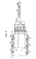
Images


Classifications
-
- H—ELECTRICITY
- H04—ELECTRIC COMMUNICATION TECHNIQUE
- H04N—PICTORIAL COMMUNICATION, e.g. TELEVISION
- H04N5/00—Details of television systems
- H04N5/14—Picture signal circuitry for video frequency region
- H04N5/21—Circuitry for suppressing or minimising disturbance, e.g. moiré or halo
Definitions
- the present invention relates to a circuit for reducing the noise contained in a video signal.
- An object of the present invention is to provide a noise reduction circuit for reducing the noise contained in video signals with suppressing the deterioration of the resolution as small as possible.
- a noise reduction circuit which comprises a plurality of delay circuits for delaying an output video signal for different delay times respectively, an average circuit for averaging the outputs of the delay circuits, a subtraction circuit for subtracting the output of the average circuit from an input video signal, an attenuation circuit for attenuating the output of subtraction circuit, an addition circuit for adding the output of the attenuation circuit to the input video signal, and an edge detection circuit for detecting the existence of the edge of a pattern in the input video signal, the attenuation factor of the attenuation circuit being controlled by the output of the edge detection circuit.
- Fig. 1 is a block diagram of a noise reduction circuit according to one embodiment of the present invention.
- Fig. 2, Fig. 4 and Fig. 5 are schematic illustrations for showing the positional relations of video signals in the picture.
- Fig. 3 is a graph showing the characteristics of the improvement of the signal-to-noise ratio against the attenuation factor.
- Fig. 6 is a block diagram of a noise reduction circuit according to another embodiment of the present invention considering the time delay in the signal processing.
- Fig. 7 is a block diagram of an example of edge detection circuit.
- Fig. 8 is a schematic illustration for showing the positional relation of video signals which are used for detecting an edge of pattern.
- Fig. 9 is a graph showing a relation between an attenuation factor of attenuation circuit and an output of the edge detection circuit.
- Fig. 1 shows the block diagram of one embodiment of the present invention.
- reference numeral 1 denotes an input terminal of video signal
- 2 denotes a subtraction circuit
- 3 denotes an attenuation circuit
- 4 denotes an addition circuit
- 5 and 6 denote delay circuits respectively
- 7 denotes an average circuit
- 8 denotes an edge detection circuit
- 9 denotes an output terminal of the video signal.
- Fig. 2 shows the positional relation in the picture between the video signal 11 taken from the input terminal of the video signal 1 and the past video signal 12 for the time 2S past and the past video signal 13. for the time H-S past from the signal 11.
- H denotes one horizontal scanning period and S designates one half of the one period of the color subcarrier.
- H is 63.565 u sec. and S is 0.140 p sec. in the NTSC system.
- Reference numerals 21 and 22 denote horizontal scanning lines and the arrow heads of the horizontal scanning lines 21 and 22 illustrate the directions of scan.
- the past video signal 12 and 13 correspond to the outputs of the delay circuits 5 and 6 shown in Fig. 1 respectively.
- the signal processing is carried out using the above mentioned three video signal 11, 12 and 13 simultaneously.
- the average circuit 7 generates the averaged signal of the output video signals 12 and 13 delayed for the time 2S and H-S respectively by the delay circuits 5 and 6.
- the difference signal between said averaged signal and the input video signal 11 is generated by the subtraction circuit 2.
- Said difference signal is multiplied by k (0 ⁇ k ⁇ 1) in the attenuation circuit 3 according to whether the edge of the pattern picked up into the video signal is detected or not between the input video signal 11 and the 2S past output video signal 12, and between the input video signal 11 and the H-S past output video signal 13.
- the difference signal is added to the input video signal 11 in the addition circuit 4 and the result of addition is taken out as the noise reduced video signal from the video signal output terminal 9.
- the above mentioned output video signal is also given to delay circuits 5 and 6 and the same performance mentioned above is repeated.
- the above mentioned output video signal is at the same position. as the above mentioned input video signal 11.
- Equation (1) the principle of the noise reduction circuit of this embodiment will be explained.
- x(t) be the input video signal given to the video signal input terminal 1 at the time t and y(t) be the output video signal taken out from the video signal output terminal 9, then equation (1) is satisfied.
- y(t-2S) and y(t-H+S) mean the 2S and H-S past output video signals respectively.
- Z s and Z H be delay operators delaying for 2S and H-S respectively and by taking the Z transform of both sides of equation (1) therefore the transfer function may be described as Although there is a relation between Z H and Z s such that they may be considered to be almost independent mutually.
- equation (5) since the video signal is described as the summation of the amplitudes of the coefficients of Z S -j Z H j-i where Now since noise is described as the summation of the power (the squares) of the coefficients of Z S -j Z H j-i , from equation (5) where the following relations are used.
- equation (11) represents the improvement factor of the signal-to-noise ratio.
- Fig. 3 shows the improvement factor of the noise reduction circuit of this embodiment against the value of the attenuation factor k where the abscissa represents the value of k and the ordinate represents the improvement factor of the signal-to-noise ratio calculated by equation (11).
- the noise reduction circuit of this embodiment because the distance in the picture between the 2S past output video signal 12 and the input video signal 11 is nearly equal to the distance in the picture between the H-S past output video signal 13 and the input video signal 11, it may be considered that the strength of the correlation between the 2S past output video signal 12 and the input video signal 11 are also nearly equal to the strength of the correlation between the H-S past video signal 13 and the input video signal 12.
- Fig. 7 is a block diagram showing an example of the edge detection circuit 8.
- reference numeral 1 denotes an input terminal of video signal
- 81 denotes a delay circuit for delaying the video signal for 1H (one horizontal scanning period)
- 82, 83, 84, 85 and 86 denote shift registers each of which delays the video signal for 1S (a half of the one period of the color subcarrier) respectively
- .87, 88, 89 and 90 denote average circuits each of which produces the average value of two signals applied thereto respectively
- 91 and 92 denote subtraction circuits each of which produces the difference value between two inputted signals respectively
- 93 denotes a comparison circuit for comparing two signals applied thereto and delivering the larger one
- 94 denotes a control circuit for generating a control signal to control the attenuation factor k of the attenuation circuit 3 (shown in Fig. 1) in accordance with the output of the comparison circuit 93.
- Fig. 8 shows the positional relation of the video signals on the displayed picture, these video signals being used for detecting the edge of pattern.
- reference numerals 21 and 22 designate horizontal scanning lines. Arrow heads of lines 21 and 22 show the directions of scan.
- the video signals 12', 13' and 14' are the past input signals for the time 2S, H-S and H+S past from the input video signal 11'.
- the outputs of the subtraction circuits 91 and 92 are These outputs (91) and (92) represent respectively the variation of video signal in the horizontal and the vertical directions on the picture.
- u be the output of the comparison circuit 93, then u may be described as and the attenuation factor k may be described as a function of u
- u and k The functional relation between u and k is illustrated in Fig. 9.
- the output u of the comparison circuit 93 is large, that is to say, the edge of pattern is detected between the signals 11' and 12' or between the signals 11' and 13', and attenuation factor k of the attenuation circuit 3 becomes zero.
- the control circuit 94 In order to change the attenuation factor k in accordance with the function of u shown in Fig. 9, the control circuit 94 generates, in response to the output u of the comparison circuit 93, a control signal for controlling the attenuation circuit 3.
- edge detection circuit Since the edge detection circuit has to discriminate the edge of pattern, namely the variation of video signal from the noise in video signal and to pick up only the variation of video signal, it is necessary for the edge detection circuit not to be affected by the noise in video signal.
- Four average circuits 87, 88, 89 and 90 in the edge detection circuit of Fig. 7 are used for reducing the influence of noise by smoothing the signal and noise.
- video signals for processing when only luminance signal is processed, video signals for processing can be selected arbitrarily from the neighboring points in the picture, but when the composite signal itself is processed, signals for processing must be selected for the phases of all of the subcarriers for color signals to be same. Therefore, in the embodiment, for the input video signal it is devised not to cancel the color signal by using for signal processing the H-S past output video signal 13 and the 2S past output video signal 12 whose phases of all the subcarriers for color signals are same. At this time, for the input video signal 11, by using the H+S past output video signal 14 shown in Fig. 4 instead of using the H-S past output video signal 13, the composite signal itself can be processed.
- the use of the H-S past output video signal 13 leads to be harder to generate noise resulting in bad picture showing such as tailing lines and good results are obtained.
- the attenuation factor is controlled adaptively to the edge part and the other flat part, the improvement of the picture quality by more than 6 dB correspondence can be attained with preserving the resolution almost completely and moreover surely reducing noise.
- the total circuit can be constructed in small size and inexpensively.
Landscapes
- Engineering & Computer Science (AREA)
- Multimedia (AREA)
- Signal Processing (AREA)
- Picture Signal Circuits (AREA)
- Processing Of Color Television Signals (AREA)
Applications Claiming Priority (2)
| Application Number | Priority Date | Filing Date | Title |
|---|---|---|---|
| JP196648/84 | 1984-09-21 | ||
| JP59196648A JPH0636602B2 (ja) | 1984-09-21 | 1984-09-21 | 雑音低減回路 |
Publications (2)
| Publication Number | Publication Date |
|---|---|
| EP0175367A2 true EP0175367A2 (de) | 1986-03-26 |
| EP0175367A3 EP0175367A3 (de) | 1987-03-18 |
Family
ID=16361267
Family Applications (1)
| Application Number | Title | Priority Date | Filing Date |
|---|---|---|---|
| EP85111866A Withdrawn EP0175367A3 (de) | 1984-09-21 | 1985-09-19 | Rauschreduzierungsschaltung |
Country Status (4)
| Country | Link |
|---|---|
| US (1) | US4636863A (de) |
| EP (1) | EP0175367A3 (de) |
| JP (1) | JPH0636602B2 (de) |
| CA (1) | CA1228671A (de) |
Cited By (1)
| Publication number | Priority date | Publication date | Assignee | Title |
|---|---|---|---|---|
| DE3927101A1 (de) * | 1989-08-17 | 1991-02-21 | Nokia Unterhaltungselektronik | Verfahren und schaltung zum bearbeiten von luminanzsignalen |
Families Citing this family (15)
| Publication number | Priority date | Publication date | Assignee | Title |
|---|---|---|---|---|
| US4833634A (en) * | 1982-11-26 | 1989-05-23 | Coblitz David B | Multipurpose adaptive filter |
| US4825295A (en) * | 1985-08-09 | 1989-04-25 | Canon Kabushiki Kaisha | Image reading apparatus |
| KR900009063B1 (ko) * | 1985-09-09 | 1990-12-17 | 니뽕 빅터 가부시끼가이샤 | 반송 색 신호 처리 회로 |
| US4853795A (en) * | 1987-07-24 | 1989-08-01 | Eastman Kodak Company | Forward look ahead techniques for tracking background and noise levels in scanned video images |
| US4982294A (en) * | 1987-07-24 | 1991-01-01 | Eastman Kodak Company | Apparatus for enhancing and thresholding scanned microfilm images and methods for use therein |
| US4833722A (en) * | 1987-07-24 | 1989-05-23 | Eastman Kodak Company | Apparatus and methods for locating edges and document boundaries in video scan lines |
| US4774569A (en) * | 1987-07-24 | 1988-09-27 | Eastman Kodak Company | Method for adaptively masking off a video window in an overscanned image |
| US5144434A (en) * | 1989-07-13 | 1992-09-01 | Canon Kabushiki Kaisha | Video signal processing device using look-up table |
| JPH0370372A (ja) * | 1989-08-10 | 1991-03-26 | Ikegami Tsushinki Co Ltd | 雑音抑圧回路 |
| JPH0372778A (ja) * | 1989-08-11 | 1991-03-27 | Fuji Xerox Co Ltd | 画像処理装置の領域識別方式 |
| US5204920A (en) * | 1990-01-12 | 1993-04-20 | U.S. Philips Corporation | Method and apparatus for region and texture coding |
| US5325203A (en) * | 1992-04-16 | 1994-06-28 | Sony Corporation | Adaptively controlled noise reduction device for producing a continuous output |
| JP3306671B2 (ja) * | 1992-09-24 | 2002-07-24 | 日本テキサス・インスツルメンツ株式会社 | ノイズ低減回路 |
| KR0181286B1 (ko) * | 1995-03-28 | 1999-05-01 | 김광호 | Ccd 카메라의 디펙트 보상회로 |
| JP3356201B2 (ja) * | 1996-04-12 | 2002-12-16 | ソニー株式会社 | ビデオカメラおよび輪郭強調装置 |
Family Cites Families (7)
| Publication number | Priority date | Publication date | Assignee | Title |
|---|---|---|---|---|
| GB1515551A (en) * | 1975-04-25 | 1978-06-28 | British Broadcasting Corp | Noise reduction in electrical signals |
| DE2962606D1 (en) * | 1978-04-03 | 1982-06-09 | British Broadcasting Corp | Noise reduction in electrical signals |
| JPS592227B2 (ja) * | 1978-08-21 | 1984-01-17 | 株式会社日立製作所 | 雑音除去方式 |
| JPS55179466U (de) * | 1979-06-11 | 1980-12-23 | ||
| JPS5827475A (ja) * | 1981-08-11 | 1983-02-18 | Hitachi Ltd | ゴ−スト除去装置 |
| DE3307687C3 (de) * | 1983-03-04 | 1994-04-28 | Broadcast Television Syst | System zur Verminderung des Rauschens in einem Fernsehsignal |
| DE3477536D1 (en) * | 1983-11-28 | 1989-05-03 | Victor Company Of Japan | Noise reduction circuit for a video signal |
-
1984
- 1984-09-21 JP JP59196648A patent/JPH0636602B2/ja not_active Expired - Lifetime
-
1985
- 1985-09-17 US US06/776,876 patent/US4636863A/en not_active Expired - Fee Related
- 1985-09-19 EP EP85111866A patent/EP0175367A3/de not_active Withdrawn
- 1985-09-23 CA CA000491347A patent/CA1228671A/en not_active Expired
Cited By (1)
| Publication number | Priority date | Publication date | Assignee | Title |
|---|---|---|---|---|
| DE3927101A1 (de) * | 1989-08-17 | 1991-02-21 | Nokia Unterhaltungselektronik | Verfahren und schaltung zum bearbeiten von luminanzsignalen |
Also Published As
| Publication number | Publication date |
|---|---|
| CA1228671A (en) | 1987-10-27 |
| JPH0636602B2 (ja) | 1994-05-11 |
| EP0175367A3 (de) | 1987-03-18 |
| JPS6175674A (ja) | 1986-04-18 |
| US4636863A (en) | 1987-01-13 |
Similar Documents
| Publication | Publication Date | Title |
|---|---|---|
| US4636863A (en) | Noise reduction circuit | |
| US4058836A (en) | Noise reduction in television signals | |
| US4524379A (en) | Double-scanning non-interlace television receiver with vertical aperture correction circuit | |
| US4241363A (en) | Comb filter circuit | |
| US4924305A (en) | Motion detecting circuit for video signal processing using correlation techniques | |
| EP0595663B1 (de) | Rauschverminderung für Videosignale | |
| EP0455434A2 (de) | Rauschverminderungsanordnungen | |
| EP0558017B1 (de) | Konturrekonstruktionsgerät | |
| US20040095476A1 (en) | Camera signal processing apparatus and camera signal processing method | |
| EP0556501B1 (de) | Videobewegungsdetektoren | |
| US4924315A (en) | Video signal processing system | |
| US5635990A (en) | Apparatus for cancelling noise and improving details of images | |
| US5225898A (en) | Noise reduction apparatus for television receiver | |
| US5225899A (en) | Correlation adaptive luminance and chrominance signal separating circuit | |
| US5715015A (en) | Method of enhancing details contained in a color signal and a circuit for implementing the same in a color video apparatus | |
| EP0196756A2 (de) | Interdimensionale Anordnung zur Reduktion des Chrominanzgeräusches | |
| EP0563877B1 (de) | Vorrichtung zum Abschneiden oder Begrenzen eines Farbsignals | |
| US5218438A (en) | Picture aperture correction circuit | |
| US6259480B1 (en) | Sequential scanning converter | |
| US4882628A (en) | Amplitude characteristics of TV vertical frequency signal | |
| EP0194759A2 (de) | Breitbandeinrichtung zur Reduktion des Chrominanzgeräusches | |
| EP0660595B1 (de) | Vorrichtung zur Rauschverminderung | |
| EP0426426B1 (de) | Filtervorrichtung | |
| JP3040251B2 (ja) | 動き検出回路 | |
| JP3350322B2 (ja) | 映像信号処理装置 |
Legal Events
| Date | Code | Title | Description |
|---|---|---|---|
| PUAI | Public reference made under article 153(3) epc to a published international application that has entered the european phase |
Free format text: ORIGINAL CODE: 0009012 |
|
| 17P | Request for examination filed |
Effective date: 19850919 |
|
| AK | Designated contracting states |
Kind code of ref document: A2 Designated state(s): DE GB |
|
| PUAL | Search report despatched |
Free format text: ORIGINAL CODE: 0009013 |
|
| AK | Designated contracting states |
Kind code of ref document: A3 Designated state(s): DE GB |
|
| 17Q | First examination report despatched |
Effective date: 19890726 |
|
| STAA | Information on the status of an ep patent application or granted ep patent |
Free format text: STATUS: THE APPLICATION HAS BEEN WITHDRAWN |
|
| 18W | Application withdrawn |
Withdrawal date: 19891102 |
|
| RIN1 | Information on inventor provided before grant (corrected) |
Inventor name: KUBOTA, SADAO Inventor name: KAIZAKI, KAZUHIROFUJIMI-RYO Inventor name: HARADA, HIROSHI Inventor name: MATSUURA, SHIGEO |