EP0173554B1 - Kathodenstrahlröhrensichtgerät - Google Patents
Kathodenstrahlröhrensichtgerät Download PDFInfo
- Publication number
- EP0173554B1 EP0173554B1 EP85306071A EP85306071A EP0173554B1 EP 0173554 B1 EP0173554 B1 EP 0173554B1 EP 85306071 A EP85306071 A EP 85306071A EP 85306071 A EP85306071 A EP 85306071A EP 0173554 B1 EP0173554 B1 EP 0173554B1
- Authority
- EP
- European Patent Office
- Prior art keywords
- horizontal
- mode
- circuit
- sensing
- display unit
- Prior art date
- Legal status (The legal status is an assumption and is not a legal conclusion. Google has not performed a legal analysis and makes no representation as to the accuracy of the status listed.)
- Expired - Lifetime
Links
- 239000003990 capacitor Substances 0.000 claims description 30
- 230000010355 oscillation Effects 0.000 claims description 9
- 239000002131 composite material Substances 0.000 claims description 4
- 230000002159 abnormal effect Effects 0.000 claims description 2
- 230000001419 dependent effect Effects 0.000 claims 1
- 238000010586 diagram Methods 0.000 description 10
- 239000013256 coordination polymer Substances 0.000 description 5
- 238000010276 construction Methods 0.000 description 4
- 238000007599 discharging Methods 0.000 description 4
- 238000000926 separation method Methods 0.000 description 4
- 230000003247 decreasing effect Effects 0.000 description 3
- 230000002265 prevention Effects 0.000 description 3
- 230000003321 amplification Effects 0.000 description 1
- 230000000903 blocking effect Effects 0.000 description 1
- 239000004403 ethyl p-hydroxybenzoate Substances 0.000 description 1
- 238000004519 manufacturing process Methods 0.000 description 1
- 238000001465 metallisation Methods 0.000 description 1
- 238000003199 nucleic acid amplification method Methods 0.000 description 1
- 239000004065 semiconductor Substances 0.000 description 1
Images
Classifications
-
- H—ELECTRICITY
- H04—ELECTRIC COMMUNICATION TECHNIQUE
- H04N—PICTORIAL COMMUNICATION, e.g. TELEVISION
- H04N5/00—Details of television systems
- H04N5/66—Transforming electric information into light information
- H04N5/68—Circuit details for cathode-ray display tubes
-
- H—ELECTRICITY
- H04—ELECTRIC COMMUNICATION TECHNIQUE
- H04N—PICTORIAL COMMUNICATION, e.g. TELEVISION
- H04N5/00—Details of television systems
- H04N5/44—Receiver circuitry for the reception of television signals according to analogue transmission standards
- H04N5/445—Receiver circuitry for the reception of television signals according to analogue transmission standards for displaying additional information
- H04N5/44504—Circuit details of the additional information generator, e.g. details of the character or graphics signal generator, overlay mixing circuits
-
- H—ELECTRICITY
- H04—ELECTRIC COMMUNICATION TECHNIQUE
- H04N—PICTORIAL COMMUNICATION, e.g. TELEVISION
- H04N3/00—Scanning details of television systems; Combination thereof with generation of supply voltages
- H04N3/10—Scanning details of television systems; Combination thereof with generation of supply voltages by means not exclusively optical-mechanical
- H04N3/16—Scanning details of television systems; Combination thereof with generation of supply voltages by means not exclusively optical-mechanical by deflecting electron beam in cathode-ray tube, e.g. scanning corrections
- H04N3/27—Circuits special to multi-standard receivers
Definitions
- the present invention relates to a CRT display unit. More particularly, the present invention relates to a CRT display unit which can be used in both of two modes, that is, a standard mode having 262.5 scanning lines for one field and a horizontal deflecting frequency of 15.754 kHz and a high-resolution mode having twice as many scanning lines as those of the standard mode and a horizontal deflecting frequency of approximately 25 kHz, this CRT display unit being utilizable as a display unit for a personal computer, a home video game set and the like.
- the vertical deflecting frequency cannot be much reduced because of the necessity of preventing flicker in the Braun tube.
- the vertical deflecting frequency can only be decreased to approximately 50 to 55 Hz.
- it is necessary to increase the horizontal deflecting frequency for example, to 24.85 kHz compared with the 15.75 kHz with 200 lines.
- Such vertical and horizontal deflecting frequencies differ greatly from those of an ordinary television set and, therefore, a high-resolution CRT display unit to be used exclusively for display is required.
- Display units of 400 lines meeting such a requirement, especially those for personal use, are in little demand and the manufacturing cost thereof tends to be high.
- a video reproducing device is disclosed in Patent Abstracts of Japan, Volume 8, No. 281 (E-286)(1718), which is adapted to select between a first mode for reproduction of T.V. signals having a first horizontal scanning frequency and a second mode for reproducing video signals from a personal computer having a second, different, horizontal scanning frequency.
- the desired mode is selected by switching circuits, but there is no disclosure in this document as to the basis on which the switching decision is made.
- selection is made between a standard mode and a "second T.V. system" mode, each having different horizontal synchronizing signals. The selection is made on the basis of the pulse width between the horizontal synchronizing signals.
- German Patent DE-C-3,331,007 discloses a television receiver operable in two modes having different respective synchronizing pulse frequencies. Mode selection is achieved by a manually operable selection switch or by remote control.
- US-A-3,994,019 discloses apparatus for discriminating between video signals from a broadcast television signal and signals from a home use video tape recorder. Discrimination is achieved by counting horizontal synchronizing pulses. In video signals from a home use video tape recorder additional pulses appear due to video head switching noises, resulting in a greater number of apparent horizontal synchronizing pulses being counted with video tape recorder signals than with broadcast television signals.
- U.S. Patent US-A-4,349,839 (McGinn) describes a television receiver adapted for reproducing video signals having one of two different numbers of lines in each frame.
- the first format has 525 lines per frame
- the second format has 625 lines per frame.
- a switch (66, see Figure 5) is used to preselect the desired mode, and, in one embodiment, this is constituted by a small strip of deposited metallisation which is present when the switch is to be closed and which is not present, i.e. is not deposited, when the switch is to be opened. Thus, whether this switch is open or closed would appear to be predetermined at the factory.
- horizontal synchronizing pulses are counted solely for the purpose of generating a vertical synchronizing signal after the appropriate number of horizontal pulses has been detected, and this appropriate number will depend upon which mode is desired.
- a CRT display unit capable of selecting between a standard mode and a high-resolution mode, characterised by the provision of: synchronizing signal separating means for separating a horizontal synchronizing signal and a vertical synchronizing signal from a composite video signal, counting means for counting said horizontal synchronizing signal, said counting means being adapted to be reset by said vertical synchronizing signal, mode sensing means for discriminating between said standard mode and said high-resolution mode of said composite video signal on the basis of the count output of said counting means, and horizontal output means for selecting between a first set and a second, different, set of values for three parameters, that is, a horizontal oscillating frequency, a horizontal amplitude and a horizontal flyback period in dependence on the mode sensed by said mode sensing means.
- a CRT display unit operable in a standard mode and in a high-resolution mode, characterised in that the unit has means for selecting the horizontal oscillation frequency, the horizontal amplitude and the horizontal flyback period for the CRT of the unit to have a first set of values appropriate for the standard mode or to have a second, different set of values appropriate for the high-resolution mode, the said means being adapted for making the said selection in dependence on a count of the number of horizontal synchronizing signals per vertical synchronizing signal in a video signal to be displayed by the unit.
- the present invention makes it possible to automatically discriminate between the respective modes and to select a horizontal oscillating frequency, a horizontal amplitude and a horizontal flyback period according to the served mode even if there is a considerable difference in the horizontal deflecting frequencies in the respective modes, which are for example, approximately 16 kHz (preferably 15.75 kHz) and approximately 25 kHz (preferably 24.85kHz).
- a time constant of the horizontal oscillating means included in the horizontal deflecting means is selected appropriately.
- switching is made to operate a time constant circuit for determining a flyback period, connected on the output side of a horizontal deflecting transistor driven by the horizontal drive means receiving the oscillation output of the horizontal oscillating means.
- the flyback period can be shortened.
- one end of a horizontal deflecting coil connected to the collector of the horizontal deflecting transistor through an S-letter correction capacitor is connected to a step-down transformer so that a horizontal amplitude according to the high-resolution mode is provided.
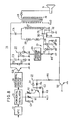
- Fig. 1 is a schematic block diagram showing the total construction of an embodiment of the present invention.
- Fig. 2 is a concrete block diagram of a line mode detecting circuit shown in Fig. 1.
- Figs. 3 and 4 are timing charts for explaining the operation of the line mode detecting circuit.
- Fig. 5 is a concrete block diagram of an erroneous operation preventing circuit shown in Fig. 1.
- Fig. 6 is a timing chart for explaining the operation of the erroneous operation preventing circuit.
- Fig. 7 is a detailed electric circuit diagram of the erroneous operation preventing circuit.
- Fig. 8 is an electric circuit diagram showing a horizontal oscillating circuit and a horizontal deflecting circuit.
- Fig. 1 is a schematic block diagram showing the total construction of a television set where an embodiment of the present invention is applied.
- An antenna 1 receives a radio wave from a broadcasting station and applies a television signal to an RF and IF amplifier 2.
- the television signal applied to the RF and IF amplifier 2 is provided to a detecting circuit 3.
- the output of the detecting circuit 3 is applied to an input selecting circuit 4.
- the input selecting circuit 4 makes selection between a television signal applied from an external apparatus such as a personal computer 5 and a television signal based on the radio wave applied through the antenna 1.
- a personal computer signal provided from the personal computer 5, as shown in the following table 1, has a line mode B or C with respect to the television signal A based on the radio wave.
- the television signal selected by the above stated input selecting circuit 4 is applied to the subsequent first video amplifier 6.
- the first video amplifier 6 amplifies the television signal to provide the video signal to a second video amplifier 7 and a synchronizing signal separation circuit 10.
- the second video amplifier 7 amplifies the video signal and applies the amplified signal to a CRT control circuit 8.
- the CRT control circuit 8 converts the video signal provided from the second video amplifier 7 from the serial signal to a parallel signal so as to enable the respective cathodes G, R and B of the CRT 9.
- the CRT control circuit 8 is adapted to enable the respective cathodes of the CRT 9 also by the respective signals RGB applied from the above stated personal computer 5.
- the synchronizing signal separation circuit 10 separates a vertical synchronizing signal F V and a horizontal synchronizing signal F H from the video signal.
- the vertical synchronizing signal F V is applied to a vertical deflecting circuit 11.
- the vertical deflecting circuit 11 drives the vertical deflecting coil of the CRT 9.
- the horizontal synchronizing signal F H is applied to a horizontal oscillating circuit 13 through an AFC 12.
- the horizontal oscillating circuit 13 provides a horizontal deflection control signal having a different oscillating frequency corresponding to the selected line mode in synchronism with the horizontal synchronizing signal F H .
- the horizonal deflection control signal provided from the horizontal oscillating circuit 13 is applied to the horizontal deflecting circuit 14.
- the horizontal deflecting circuit 14 enables the horizontal deflecting coil of the CRT 9 based on the horizontal deflection control signal.
- the television set comprises a line mode detecting circuit 17, a switching circuit 18 and an erroneous operation preventing circuit 19.
- the horizontal synchronizing signal F H and the vertical synchronizing signal F V are applied.
- the line mode detecting circuit 17 detects the respective modes.
- the switching circuit 18 selects a horizontal oscillating frequency for the horizontal oscillating circuit 13 according to the detected mode and also selects a horizontal flyback period and a horizontal amplitude for the horizontal deflecting circuit 14 according to the detected mode.
- the erroneous operation preventing circuit 19 prevents the switching circuit 18 from erroneously operating due to noise contained in the video signal.
- Fig. 2 is a specific block diagram of the line mode detecting circuit shown in Fig. 1 and Figs. 3 and 4 are timing charts for explaining the operation of the line mode detecting circuit.
- the line mode detecting circuit 17 comprises a counter 179, an AND circuit 180, a detector 181 and an integrator 182, as shown in Fig. 2.
- the counter 179 counts the number of pulses of the horizontal synchronizing signal F H provided from the above stated synchronizing separation circuit 10 and is set by the vertical synchronizing signal F V .
- This counter 179 comprises nine stages of binary counters 170 to 178.
- the AND circuit 180 has three input terminals to which are connected, respectively, the count output 2 5 of the counter 175 in the sixth stage, the count output 2 7 of the counter 177 in the eighth stage and the count output 2 8 of the counter 178 in the ninth stage, these three counters being included in the counter 179.
- the integrator 182 is connected through the detector 181.
- the integrator 182 is characterized by a short charging time and a long discharging time.
- the charging time is equal to an output period of the AND circuit 180, that is, a pulse period of the vertical synchronizing signal F V and a discharging time constant T is set to more than a half cycle T V /2 of the vertical synchronizing signal F V so as to prevent erroneous operation due to lowering of the output of the AND circuit 3.
- the output of the integrator 182 is applied to the above stated switching circuit 18.
- the switching circuit 18 comprises a semiconductor circuit, for example, a CMOS logic circuit with a threshold level set to approximately 1/2 of the supplied voltage, so that the output thereof falls to a low level in the case of the input thereof higher than a predetermined threshold level and rises to a high level in the case of the input thereof lower than the threshold level.
- a semiconductor circuit for example, a CMOS logic circuit with a threshold level set to approximately 1/2 of the supplied voltage, so that the output thereof falls to a low level in the case of the input thereof higher than a predetermined threshold level and rises to a high level in the case of the input thereof lower than the threshold level.
- the operation of the line mode detecting circuit 17 thus constructed will be described in the following.
- a personal computer signal having 448 lines for one frame as shown in Table 1C for example is applied from the personal computer 5
- the counter 179 counts each time a horizontal synchronizing signal F H is applied to the counter 179 from the personal computer 5.
- the counter 178 in the last stage namely, in the ninth stage, provides an output which attains the high level only after the receipt of the 256th horizontal synchronizing signal F H .
- the counter 178 is reset by the vertical synchronizing signal F V applied simultaneously with the 440th horizontal synchronizing signal F H , so that the output thereof returns to the low level.
- the output of the AND circuit 180 attains the high level so that the integrator 182 is charged.
- the output of the AND circuit 180 falls to the low level and all the outputs of the counters 175, 177 and 178 in the sixth, eighth and ninth stages respectively attain again the low level, so that the integrator 182 is discharged till the output of the AND circuit 180 rises to the high level.
- the discharging time constant of the integrator 182 is set to more than 1/2 of the vertical synchronizing cycle T V , charging operation is repeated in a period after the start of discharging of the integrator 182 before the lowering of the output level to 1/2 of the supplied voltage and consequently, the output of the integrator 182 is provided as a mode signal V M of a high level maintained higher than the threshold level of the switching circuit 18.
- the input selecting circuit 4 selects a television signal based on a radio wave instead of the above stated personal computer signal from the personal computer 5.
- the output of the counter 178 in the ninth stage is at the low level till the 255th horizontal synchronizing signal F H is received.
- the output of the counter 178 is at the high level till the vertical synchronizing signal F V is received simultaneously with the 258th horizontal synchronizing signal.
- the outputs of the counters 177 and 175 in the eighth and sixth stages respectively are changed to the low level in the period after the receipt of the 256th horizontal synchronizing signal till the receipt of the vertical synchronizing signal F V .
- the output level is provided as the mode signal V M of a low level lower than the threshold level of the switching circuit 18.
- the output of the switching circuit 18 is of a low value, so that the horizontal oscillating frequency and the oscillating frequency of the horizontal oscillating circuit 13 associated with the operation of the deflecting circuit are changed to correspond to the personal computer signal shown in Table 1C. Also in the horizontal deflecting circuit 14, the horizontal amplitude and the horizontal flyback period are changed. This changing operation will be described later in detail with reference to Fig. 8.
- Fig. 5 is a specific block diagram of the erroneous operation preventing circuit shown in Fig. 1;
- Fig. 6 is a timing chart for explaining the operation of the erroneous operation preventing circuit;
- Fig. 7 is a detailed electric circuit diagram of the erroneous operation preventing circuit.
- a pulse due to the noise could be mixed in the horizontal synchronizing signal F H provided from the synchronizing separation circuit 10, resulting in erroneous operation of the line mode detecting circuit 17 which counts the number of pulses of the horizontal synchronizing sighal F H .
- the apparent number of pulses of the horizontal synchronizing signal becomes considerably larger than the real number of pulses of the horizontal synchronizing signal and the counter 179 might count the number of pulses corresponding to a different line mode to cause error in determination of a line mode by the AND circuit 180.
- the personal computer signal in Table A is selected by the input selecting circuit 10
- the horizontal oscillator B and the horizontal deflecting circuit 14 might be switched by the switching circuit 18 to correspond to the line mode erroneously determined by that television signal.
- the erroneous operation preventing circuit 19 comprises a noise level detecting circuit 191 and an erroneous operation prevention signal providing circuit 194 as shown in Fig. 5.
- the noise level detecting circuit 191 comprises a noise amplifier 192 and a detector 193.
- the noise amplifier 192 receives from the second video amplifier 10, a video signal containing noise as shown in Fig. 6(a) and amplifies mainly the synchronizing signal by a bias approximate to the class B amplification.
- the detector 193 comprises, as shown in Fig. 7 for example, a diode detector and the like connected to the output of the noise amplifier 192 through a capacitor C for blocking direct current.
- the detector 193 receives the output of the noise amplifier 192 as shown in Fig. 6(b) and provides detected voltage as shown in Fig. 6(d).
- the output voltage of the detector 193 rises in synchronism with the rise of the horizontal synchronizing signal and the receipt of the noise and when this output voltage exceeds the voltage corresponding to the noise level which makes the apparent number of pulses of the horizontal synchronizing signal twice as large as the real number thereof for example, the erroneous operation prevention signal providing circuit 194 is caused to provide an erroneous operation prevention signal as shown in Fig. 6(e).
- the erroneous operation preventing circuit 19 makes it possible to completely prevent the erroneous operation, that is, the supply of an erroneous mode signal due to the wrong determination of a line mode caused by counting the apparent number of pulses of the horizontal synchronizing signal larger than the real number thereof in the case where a noise signal contained in a video signal is applied to the counter 179 of the line mode detecting circuit 17.
- Fig. 8 is an electric circuit diagram showing the horizontal oscillator and the horizontal deflecting circuit.
- a horizontal oscillating frequency selecting circuit 21 for selecting a horizontal oscillating frequency according to each mode is provided in association with the horizontal oscillator 13.
- the horizontal oscillator 13 is provided with resistors R1 and R2 and a capacitor C1 externally so that an oscillating frequency can be determined by the time constants thereof. More specifically, in the standard mode, the resistor R1 and the capacitor C1 are connected to make oscillation with the horizontal deflecting frequency f1 and the time constant is 1/R1 ⁇ C1.
- the transistor Q1 is rendered conductive and the resistors R1, R2 and the capacitor C1 are connected externally to oscillate with the horizontal deflecting frequency f2, the time constant being 1/[(R1//R2) ⁇ C1].
- the transistor Q1 is controlled so that it changes rapidly from the non-conducting state to the conducting state, that is, from the state of oscillation with the horizontal deflecting frequency f1 to the state of oscillation with the horizontal deflecting frequency f2 and changes slowly from the conducting state to the non-conducting state. More specifically, in order to change the time constant at the time of conducting and non-conducting states of the transistor Q1, the resistors R3, R4, R5, a capacitor C2 and a diode D1 are connected.
- the transistor Q1 is conductive when the transistor Q2 controlled by the switching control signal from the switching circuit 18 shown in Fig. 1 is conductive.
- the oscillation output of the horizontal oscillator 13 is applied to a horizontal drive circuit 20.
- a horizontal deflecting transistor Q3 is connected to the output of the horizontal drive circuit 20.
- a horizontal flyback period selecting circuit 22 is connected to the collector of the horizontal deflecting transistor Q3, and capacitors C3 and C4 are connected in series.
- a cathode of a bias diode D3 and an anode of a thyristor 24 are connected to the point of connection of the capacitors C3 and C4.
- an anode of the diode D3 and a cathode of the thyristor 24 are connected to the emitter of the horizontal deflecting output transistor Q3, an anode of the diode D3 and a cathode of the thyristor 24 are connected.
- the gate of the thyristor 24 is connected to a thyristor drive circuit 25.
- the thyristor 24 In response to a gate signal from the thyristor drive circuit 25, the thyristor 24 is conducted in the standard mode to bring the capacitor C4 into a short-circuited state. As a result, the capacitance for determining a horizontal flyback period is determined only by the capacity C3. On the other hand, the thyristor 24 is in the non-conductive state in the high-resolution mode and the horizontal flyback period is made shorter than that in the standard mode as the capacitance for determining the horizontal flyback period is set to C3 ⁇ C4/(C3 + C4).
- a flyback transformer 26 is connected and an end of a deflecting coil 28 and an end of a step-down transformer 27 are also connected through the S-letter correction capacitor C5.
- the other end of the step-down transformer 27 is grounded and an intermediate tap 29 thereof is connected to one contact of a relay 30.
- the other contact of the relay 30 is grounded and a common contact is connected to the other end of the deflecting coil 28.
- the relay 30 selects a horizontal amplitude in the standard mode and that in the high-resolution mode.
- An end of a coil 31 of the relay 30 is connected to a DC power source 32 and the other end thereof is connected to the collector of the above-stated transistor Q2. Further, a protection circuit 23 is connected to the common contact of the relay 30.
- the protection circuit 23 comprises diodes D4, D5, resistors R6, R7 and capacitors C6 and C7. The protection circuit 23 is temporarily opened at the time of switching the contact of the relay 30 and an abnormal pulse of high voltage generated at this time in the horizontal deflecting coil 28 is absorbed by the protection circuit 23.
- the diode D4 and the capacitor C6 included in the protection circuit 23 constitute a rectifier, which rectifies pulse voltage generated at the time of switching the contact of the relay 30 from the ground side to the side of the intermediate tap 29 of the step-down transformer 27, so as to apply DC voltage to the thyristor drive circuit 25.
- I CP V CC ⁇ T/L (1)
- V CC power source voltage
- T is a conduction period of the horizontal output transistor Q3
- L is a synthesized inductance
- T H is a horizontal cycle
- T R is a flyback period
- C is a synthesized capacitance of the capacitors C3 and C4.
- this order of selection can be established by arranging the horizontal oscillator and the horizontal output circuit as shown in Fig. 8.
- the horizontal oscillator 13 oscillates with the frequency f1 determined by the time constants of the external resistor R1 and capacitor C1.
- the transistor Q2 is conducted and as a result, the transistor Q1 is conducted, whereby the resistor R2 is connected in parallel with the resistor R1.
- the horizontal oscillator 13 oscillates with the frequency f2 corresponding to the high-resolution mode.
- the contact of the relay 30 is turned to the side of the intermediate tap 29 of the step-down transformer 27.
- the deflecting coil 28 is set to the horizontal amplitude stepped down by the step-down transformer 27. Since the contact of the relay 30 is turned to the side of the intermediate tap 29 of the step-down transformer 27, a pulse is provided at the common contact. This pulse is rectified and stabilized by the diode D4 and the capacitor C6 so that a predetermined gate voltage is generated by the thyristor drive circuit 25. The thyristor 4 is conducted by this gate voltage to bring the capacitor C4 into a short-circuited state. As a result, only the resonance capacitance of the capacitor C3 is connected between the collector and the emitter of the horizontal output transistor Q3. Accordingly, the horizontal flyback period corresponding to the standard mode is selected.
- the transistor Q2 is conducted.
- the transistor Q1 is also conducted and the horizontal oscillator 13 is connected in parallel with the externally provided resistors R1 and R2.
- the horizontal oscillator 13 oscillates with the frequency f2 corresponding to the high-resolution mode, with the time constants determined by the resistors R1 and R2 and the capacitor C1.
- conduction of the transistor Q2 causes electric current to flow in the coil 31 of the relay 30 so that the contact of the relay 30 is turned from the side of the intermediate tap 29 to the ground side.
- the deflecting coil 28 is not stepped down by the step-down transformer 27 so that the horizontal amplitude corresponds to the high-resolution mode.
- the thyristor 24 is brought into the non-conductive state. Then, the resonance capacitance of the capacitors C3 and C4 are caused to be connected between the collector and the emitter of the horizontal output transistor Q3, whereby the horizontal flyback period corresponding to the high resolution mode is selected.
- the line mode detecting circuit 17 detects the change from the high-resolution mode to the standard mode, the transistor Q2 becomes non-conductive. However, since the time constant circuit is provided to make the transistor Q1 change slowly from the conductive state to the non-conductive state, the transistor Q1 is not immediately brought into the non-conductive state although the transistor Q2 becomes non-conductive. As a result of the non-conductive state of the transistor Q2, electric current stops flowing in the coil 31 side of the intermediate tap 29 of the step-down transformer 27. Consequently, the horizontal amplitude corresponding to the standard mode is selected.
- the contact of the relay 30 being connected to the side of the intermediate tap 29 causes a pulse at the common contact.
- the pulse is rectified and stabilized by the diode D4 and the capacitor C6 and the thyristor 24 is rendered conductive by the gate voltage according to the DC voltage.
- the capacitor C4 is short-circuited and the resonance capacitance is formed only by the capacitor C3, whereby the horizontal flyback period corresponding to the standard mode is selected.
- the transistor Q1 for selecting the oscillating frequency of the horizontal oscillator 13 is rendered non-conducting, and the external resistor R2 is separated, so that the horizontal oscillator 13 oscillates with the frequency f1 corresponding to the standard mode, with the time constants determined by the external resistor R1 and capacitor C1.
- a change from the standard mode to the high-resolution mode is made according to the order of selection of the horizontal oscillating frequency, the horizontal amplitude and the resonance capacitance, and change from the high-resolution mode to the standard mode is made according to the order of selection of the horizontal amplitude, the resonance capacitance and the horizontal oscillating frequency.
Landscapes
- Engineering & Computer Science (AREA)
- Multimedia (AREA)
- Signal Processing (AREA)
- Computer Graphics (AREA)
- Details Of Television Scanning (AREA)
Claims (10)
- Kathodenstrahlröhren-Anzeigeeinheit mit Auswahlmöglichkeit zwischen einer Standardbetriebsart und einer hochauflösenden Betriebsart,
gekennzeichnet durch:- eine Synchronsignal-Abtrennschaltung (10) zum Abtrennen eines Horizontalsynchronsignals und eines Vertikalsynchronsignals aus einem zusammengesetzten Videosignal.- eine Zahleinrichtung (179) zum Zählen der Horizontalsynchronsignale, die durch das Vertikalsynchronsignal rückgesetzt wird.- einen Betriebsartsensor (180) zum Unterscheiden zwischen der Standardbetriebsart und der hochauflösenden Betriebsart des zusammengesetzten Videosignals auf Grund des von der Zähleinrichtung ausgegebenen Zählwerts, und- eine Horizontalausgabeeinrichtung (13 und 14), die abhängig von der durch den Betriebsartsensor festgestellten Betriebsart, eine Auswahl trifft zwischen einem ersten und einem zweiten unterschiedlichen Wertesatz für drei Parameter, nämlich einer Horizontalschwingungsfrequenz, einer Horizontalamplitude und einer Horizontalrücklaufperiode. - Kathodenstrahlröhren-Anzeigeeinheit nach Anspruch 1, bei der die Horizontalausgabeeinrichtung eine Einrichtung (21, 22 und 23) aufweist, zum Auswählen zunächst der Horizontalschwingungsfrequenz aus den drei Parametern, entsprechend der hochauflösenden Betriebsart, wenn der Betriebsartsensor eine Änderung von der Standardbetriebsart auf die hochauflösende Betriebsart feststellt, und zum Auswählen der Horizontalschwingungsfrequenz aus den drei Parametern, wenn der Betriebsartsensor eine Änderung von der hochauflösenden Betriebsart in die Standardbetriebsart feststellt.
- Kathodenstrahlröhren-Anzeigeeinheit nach Anspruch 1 oder Anspruch 2, bei der- die Horizontalausgabeeinrichtung folgende Baugruppen aufweist:-- einen Horizontaloszillator (13) zum Erzeugen eines Horizontalschwingungssignals und-- eine Einrichtung (21) zum Ändern der Schwingungsfrequenz des Horizontaloszillators bei Feststellung einer Änderung in die hochauflösende Betriebsart durch den Betriebsartsensor.
- Kathodenstrahlröhren-Anzeigeeinheit nach Anspruch 3, bei der- der Horizontaloszillator eine Zeitkonstantenschaltung (R1, R2 und C1) aufweist, und- die Einrichtung zum Ändern der Schwingungsfrequenz eine Schalteinrichtung (Q1) aufweist, die bei Feststellung der Änderung in die hochauflösende Betriebsart durch den Betriebsartsensor leitend geschaltet wird, wodurch die Zeitkonstanten der Zeitkonstantenschaltung ausgewählt werden.
- Kathodenstrahlröhren-Anzeigeeinheit nach Anspruch 3, bei der- die Horizontalausgabeeinrichtung folgendes aufweist:-- einen Horizontaltreiber (20), der das Ausgangssignal des Horizontaloszillators übernimmt,-- einen vom Horizontaltreiber gesteuerten Horizontalablenktransistor (Q3).-- eine Zeitkonstantenschaltung (C3 und C4), die mit dem Ausgang des Horizontalablenktransistors verbunden ist und die Horizontalrücklaufperiode bestimmt, und-- eine Einrichtung (24) zum Auswählen der Konstanten der Zeitkonstantenschaltung, wenn der Betriebsartsensor eine Änderung in die hochauflösende Betriebsart feststellt.
- Kathodenstrahlröhren-Anzeigeeinheit nach Anspruch 5, bei der- die Zeitkonstantenschaltung einen ersten Kondensator (C3) und einen zweiten Kondensator (C4) aufweist, die in Reihe zwischen den Kollektor und den Emitter des Horizontalablenktransistors geschaltet sind,- die Auswahleinrichtung folgendes aufweist:-- eine Diode (D3), deren Kathoden mit einem Verbindungspunkt zwischen dem ersten und dem zweiten Kondensator verbunden ist und deren Anode an den Emitter des Horizontalablenktransistors angeschlossen ist,-- einen Thyristor (24), dessen Anode mit einem Verbindungspunkt zwischen dem ersten und zweiten Kondensator verbunden ist und dessen Kathode an den Emitter des Horizontalablenktransistors angeschlossen ist, und-- eine Schaltung (25), die bei Feststellung Änderung in die hochauflösende Betriebsart durch den Betriebsartsensor das Gate des Thyristors mit einem Gatesignal beaufschlagt.
- Kathodenstrahlröhren-Anzeigeeinheit nach Anspruch 5 oder Anspruch 6, bei der- die Horizontalausgabeeinrichtung folgendes aufweist:-- einen Kondensator (C5) für S-Korrektur, angeschlossen an den Kollektor des Horizontalablenktransistors,-- eine Horizontalablenkspule (28), deren eines Ende mit dem anderen Ende des Kondensators für die S-Korrektur verbunden ist.-- eine Abwärtstransformator (27) mit einem Mittelabgriff (29), dessen eines Ende mit dem anderen Ende des Kondensators für die S-Korrekturverbunden ist, und-- eine Auswahleinrichtung (30) zum Auswählen der Horizontalamplitude durch Verbinden des anderen Endes der Horizontalablenkspule mit dem Mittelabgriff des Abwärtstransformators auf die Feststellung einer Änderung in die hochauflösende Betriebsart durch den Betriebsartsensor.
- Kathodenstrahlröhren-Anzeigeeinheit nach Anspruch 7, bei der- die Auswahleinrichtung ein Relais (31) mit einem Kontakt (30) aufweist, der zwischen das andere Ende der Horizontalablenkspule und den Abwärtstransformator geschaltet ist und der abhängig von der Betriebsart geschlossen ist, wie sie vom Betriebsartsensor festgestellt wird, und- eine Schutzschaltung (23) vorhanden ist, die mit dem anderen Ende der Horizontalablenkspule verbunden ist, um einen abnormalen Puls zu absorbieren, wie er beim Öffnen und Schließen des Relaiskontakts erzeugt wird.
- Kathodenstrahlröhren-Anzeigeeinheit nach einem der vorangehenden Ansprüche mit:- einem Rauschpegel-Detektor (191) zum Feststellen des Rauschpegels im Videosignal, und- eine Sperreinrichtung (194), welche die Auswahl der Horizontalablenkeinrichtung abhängig von der jeweiligen Betriebsart unterbindet, wenn der vom Rauschpegel-Detektor ermittelte Rauschpegel einen vorgegebenen Wert überschreitet.
- Kathodenstrahlröhren-Anzeigeeinheit, die in einer Standardbetriebsart und einer hochauflösenden Betriebsart betreibbar ist, gekennzeichnet durch einen Einrichtung (13, 14, 17) zum Auswählen der Horizontalschwingungsfrequenz, der Horizontalamplitude und der Horizontalrücklaufperiode für die Kathodenstrahlröhre, die einem ersten bzw. zweiten Satz von Werten zugeordnet sind, die für die Standardbetriebsart bzw. für die hochauflösende Betriebsart passend sind, wobei die Einrichtung (13, 14, 17) die Auswahl abhängig vom Zählwert der Anzahl von Horizontalsynchronsignalen pro Vertikalsynchronsignal eines von der Einheit darzustellenden Videosignals trifft.
Applications Claiming Priority (8)
| Application Number | Priority Date | Filing Date | Title |
|---|---|---|---|
| JP1984133023U JPS6147559U (ja) | 1984-08-31 | 1984-08-31 | 水平偏向回路 |
| JP133023/84U | 1984-08-31 | ||
| JP223477/84 | 1984-10-23 | ||
| JP59223477A JPS61101174A (ja) | 1984-10-23 | 1984-10-23 | 水平偏向回路 |
| JP224853/84 | 1984-10-24 | ||
| JP59224853A JPS61100791A (ja) | 1984-10-24 | 1984-10-24 | Crt表示装置 |
| JP200021/84U | 1984-12-25 | ||
| JP1984200021U JPS61111256U (de) | 1984-12-25 | 1984-12-25 |
Publications (3)
| Publication Number | Publication Date |
|---|---|
| EP0173554A2 EP0173554A2 (de) | 1986-03-05 |
| EP0173554A3 EP0173554A3 (en) | 1988-01-07 |
| EP0173554B1 true EP0173554B1 (de) | 1991-11-21 |
Family
ID=27471737
Family Applications (1)
| Application Number | Title | Priority Date | Filing Date |
|---|---|---|---|
| EP85306071A Expired - Lifetime EP0173554B1 (de) | 1984-08-31 | 1985-08-27 | Kathodenstrahlröhrensichtgerät |
Country Status (9)
| Country | Link |
|---|---|
| US (1) | US4684987A (de) |
| EP (1) | EP0173554B1 (de) |
| KR (1) | KR890004223B1 (de) |
| AU (1) | AU578194B2 (de) |
| BR (1) | BR8504215A (de) |
| CA (1) | CA1244932A (de) |
| DE (1) | DE3584704D1 (de) |
| ES (1) | ES8700767A1 (de) |
| PH (1) | PH23162A (de) |
Families Citing this family (12)
| Publication number | Priority date | Publication date | Assignee | Title |
|---|---|---|---|---|
| JPH0646783B2 (ja) * | 1984-10-15 | 1994-06-15 | ソニー株式会社 | マルチ走査形テレビジヨン受像機 |
| US4686698A (en) * | 1985-04-08 | 1987-08-11 | Datapoint Corporation | Workstation for interfacing with a video conferencing network |
| AU588372B2 (en) * | 1985-09-20 | 1989-09-14 | Aurotech N.L. | Precious metal extraction |
| US4991023A (en) * | 1989-05-22 | 1991-02-05 | Hewlett-Packard Company | Microprocessor controlled universal video monitor |
| US5742265A (en) * | 1990-12-17 | 1998-04-21 | Photonics Systems Corporation | AC plasma gas discharge gray scale graphic, including color and video display drive system |
| US5154171A (en) | 1991-06-15 | 1992-10-13 | Raul Chirife | Rate adaptive pacemaker controlled by ejection fraction |
| JPH0594146A (ja) * | 1991-10-02 | 1993-04-16 | Mitsubishi Electric Corp | 輝度制御回路 |
| US5767917A (en) * | 1996-04-30 | 1998-06-16 | U.S. Philips Corporation | Method and apparatus for multi-standard digital television synchronization |
| KR100223644B1 (ko) * | 1997-01-14 | 1999-10-15 | 윤종용 | 개인용 컴퓨터 모니터 겸용 멀티시스템 텔레비젼 수상기 |
| US6037994A (en) * | 1997-05-09 | 2000-03-14 | Lg Electronics, Inc. | Sync signal processing device for combined video appliance |
| US6894706B1 (en) * | 1998-09-18 | 2005-05-17 | Hewlett-Packard Development Company, L.P. | Automatic resolution detection |
| JP2009253539A (ja) * | 2008-04-03 | 2009-10-29 | Panasonic Corp | 垂直同期制御装置 |
Family Cites Families (10)
| Publication number | Priority date | Publication date | Assignee | Title |
|---|---|---|---|---|
| CA1017443A (en) * | 1973-11-26 | 1977-09-13 | Takayuki Sagishima | Vtr signal discriminating apparatus in a television receiver |
| NL7714397A (nl) * | 1977-12-27 | 1979-06-29 | Philips Nv | Omschakelbare synchroniseer-signaalgenerator geschikt voor meerdere televisiestandaarden. |
| US4316219A (en) * | 1980-07-17 | 1982-02-16 | Rca Corporation | Synchronizing circuit adaptable for various TV standards |
| US4414571A (en) * | 1980-10-09 | 1983-11-08 | Matsushita Electric Industrial Co., Ltd. | Television receiver |
| US4349839A (en) * | 1980-12-29 | 1982-09-14 | Motorola, Inc. | Vertical sync counter having multi modes of operation for different TV systems standards |
| US4616260A (en) * | 1983-02-28 | 1986-10-07 | Data General Corporation | Terminal having user selectable faster scanning |
| DE3331007C1 (de) * | 1983-08-27 | 1984-08-23 | Loewe Opta Gmbh, 8640 Kronach | Fernsehempfangsgerät in Verbindung mit einem Textdecoder, wie Bildschirmtext- oder Videotext-Decoder |
| GB2148652B (en) * | 1983-09-15 | 1987-09-09 | Sinclair Res Ltd | Television receivers |
| JPS60251777A (ja) * | 1984-05-29 | 1985-12-12 | Sony Corp | 垂直偏向信号の振幅検出回路 |
| US4727362A (en) * | 1984-07-16 | 1988-02-23 | International Business Machines Corporation | Digital display system |
-
1985
- 1985-07-18 AU AU45169/85A patent/AU578194B2/en not_active Expired
- 1985-07-25 CA CA000487521A patent/CA1244932A/en not_active Expired
- 1985-08-02 PH PH32601A patent/PH23162A/en unknown
- 1985-08-16 US US06/766,334 patent/US4684987A/en not_active Expired - Lifetime
- 1985-08-27 DE DE8585306071T patent/DE3584704D1/de not_active Expired - Lifetime
- 1985-08-27 EP EP85306071A patent/EP0173554B1/de not_active Expired - Lifetime
- 1985-08-30 KR KR1019850006321A patent/KR890004223B1/ko not_active Expired
- 1985-08-30 ES ES85546620A patent/ES8700767A1/es not_active Expired
- 1985-08-30 BR BR8504215A patent/BR8504215A/pt not_active IP Right Cessation
Also Published As
| Publication number | Publication date |
|---|---|
| PH23162A (en) | 1989-05-19 |
| AU578194B2 (en) | 1988-10-13 |
| AU4516985A (en) | 1986-03-06 |
| KR890004223B1 (ko) | 1989-10-27 |
| BR8504215A (pt) | 1986-07-01 |
| EP0173554A2 (de) | 1986-03-05 |
| CA1244932A (en) | 1988-11-15 |
| US4684987A (en) | 1987-08-04 |
| DE3584704D1 (de) | 1992-01-02 |
| ES546620A0 (es) | 1986-10-16 |
| ES8700767A1 (es) | 1986-10-16 |
| KR860002195A (ko) | 1986-03-26 |
| EP0173554A3 (en) | 1988-01-07 |
Similar Documents
| Publication | Publication Date | Title |
|---|---|---|
| EP0173554B1 (de) | Kathodenstrahlröhrensichtgerät | |
| US4679091A (en) | Multiple scanning type television receiver | |
| US4673984A (en) | Multiple scanning type television receiver | |
| US4588929A (en) | Power supply and deflection circuit providing multiple scan rates | |
| US3378775A (en) | Method and apparatus for controlling a television receiver | |
| EP0520312B1 (de) | Ausschaltung für einen Fernsehsynchronisator oder Phasendetektor | |
| JP2845879B2 (ja) | ビデオ装置 | |
| CA1064580A (en) | Automatic fine tuning circuit | |
| US3819955A (en) | Counter circuit using current source | |
| US4047078A (en) | Pulse differentiating high voltage shutdown circuit | |
| US4365270A (en) | Dual standard vertical deflection system | |
| US4435731A (en) | Television receiver disabling circuit | |
| US3629497A (en) | Stabilized power supply with dc voltage step-down for transistorized television receivers and the like | |
| US3584141A (en) | Automatic tuning device for television receiver | |
| EP0444781A2 (de) | Fernsehempfänger und Verfahren in diesem | |
| US4999707A (en) | Synchronizing signal separating circuit separating synchronizing signal from a composite video signal | |
| US4599673A (en) | Degaussing system arrangements | |
| KR100233892B1 (ko) | 멀티미디어 텔레비전 수상장치 | |
| US3893032A (en) | Channel selection device | |
| EP0024860A2 (de) | Vertikalablenkung für ein Zweinormenfernsehsystem | |
| JPH05211618A (ja) | 偏向回路 | |
| EP0390183B1 (de) | Synchronisationssignal-Abtrennschaltung | |
| US3715493A (en) | Service switch arrangement for improved interlace performance | |
| KR0137279B1 (ko) | 수직 편향 회로 | |
| JPS6151828B2 (de) |
Legal Events
| Date | Code | Title | Description |
|---|---|---|---|
| PUAI | Public reference made under article 153(3) epc to a published international application that has entered the european phase |
Free format text: ORIGINAL CODE: 0009012 |
|
| AK | Designated contracting states |
Kind code of ref document: A2 Designated state(s): DE FR GB |
|
| PUAL | Search report despatched |
Free format text: ORIGINAL CODE: 0009013 |
|
| AK | Designated contracting states |
Kind code of ref document: A3 Designated state(s): DE FR GB |
|
| 17P | Request for examination filed |
Effective date: 19880229 |
|
| 17Q | First examination report despatched |
Effective date: 19891213 |
|
| GRAA | (expected) grant |
Free format text: ORIGINAL CODE: 0009210 |
|
| AK | Designated contracting states |
Kind code of ref document: B1 Designated state(s): DE FR GB |
|
| REF | Corresponds to: |
Ref document number: 3584704 Country of ref document: DE Date of ref document: 19920102 |
|
| ET | Fr: translation filed | ||
| PLBI | Opposition filed |
Free format text: ORIGINAL CODE: 0009260 |
|
| 26 | Opposition filed |
Opponent name: INTERESSENGEMEINSCHAFT FUER RUNDFUNKSCHUTZRECHTE E Effective date: 19920820 |
|
| PGFP | Annual fee paid to national office [announced via postgrant information from national office to epo] |
Ref country code: FR Payment date: 19930805 Year of fee payment: 9 |
|
| PGFP | Annual fee paid to national office [announced via postgrant information from national office to epo] |
Ref country code: GB Payment date: 19930817 Year of fee payment: 9 |
|
| PGFP | Annual fee paid to national office [announced via postgrant information from national office to epo] |
Ref country code: DE Payment date: 19930823 Year of fee payment: 9 |
|
| RDAG | Patent revoked |
Free format text: ORIGINAL CODE: 0009271 |
|
| STAA | Information on the status of an ep patent application or granted ep patent |
Free format text: STATUS: PATENT REVOKED |
|
| 27W | Patent revoked |
Effective date: 19931025 |
|
| GBPR | Gb: patent revoked under art. 102 of the ep convention designating the uk as contracting state |
Free format text: 931025 |