EP0172425B1 - Circuit synthétiseur de fréquence - Google Patents
Circuit synthétiseur de fréquence Download PDFInfo
- Publication number
- EP0172425B1 EP0172425B1 EP19850109137 EP85109137A EP0172425B1 EP 0172425 B1 EP0172425 B1 EP 0172425B1 EP 19850109137 EP19850109137 EP 19850109137 EP 85109137 A EP85109137 A EP 85109137A EP 0172425 B1 EP0172425 B1 EP 0172425B1
- Authority
- EP
- European Patent Office
- Prior art keywords
- signal
- phase
- output
- signals
- frequency
- Prior art date
- Legal status (The legal status is an assumption and is not a legal conclusion. Google has not performed a legal analysis and makes no representation as to the accuracy of the status listed.)
- Expired
Links
- 230000000295 complement effect Effects 0.000 claims description 9
- 238000005070 sampling Methods 0.000 claims description 3
- 238000010586 diagram Methods 0.000 description 17
- 230000006870 function Effects 0.000 description 12
- 238000000034 method Methods 0.000 description 11
- 230000008901 benefit Effects 0.000 description 5
- 238000013461 design Methods 0.000 description 5
- 230000000694 effects Effects 0.000 description 5
- 230000009897 systematic effect Effects 0.000 description 5
- 238000012935 Averaging Methods 0.000 description 4
- 230000008859 change Effects 0.000 description 4
- 238000005259 measurement Methods 0.000 description 4
- 230000007704 transition Effects 0.000 description 4
- 230000000712 assembly Effects 0.000 description 3
- 238000000429 assembly Methods 0.000 description 3
- 230000002238 attenuated effect Effects 0.000 description 3
- 239000003990 capacitor Substances 0.000 description 3
- 238000002955 isolation Methods 0.000 description 2
- 238000012986 modification Methods 0.000 description 2
- 230000004048 modification Effects 0.000 description 2
- 230000010363 phase shift Effects 0.000 description 2
- 230000008569 process Effects 0.000 description 2
- 230000002441 reversible effect Effects 0.000 description 2
- 230000000630 rising effect Effects 0.000 description 2
- 230000001360 synchronised effect Effects 0.000 description 2
- 238000012360 testing method Methods 0.000 description 2
- 230000018199 S phase Effects 0.000 description 1
- 230000001276 controlling effect Effects 0.000 description 1
- 238000012937 correction Methods 0.000 description 1
- 230000008878 coupling Effects 0.000 description 1
- 238000010168 coupling process Methods 0.000 description 1
- 238000005859 coupling reaction Methods 0.000 description 1
- 239000013078 crystal Substances 0.000 description 1
- 230000001934 delay Effects 0.000 description 1
- 238000001514 detection method Methods 0.000 description 1
- 230000009977 dual effect Effects 0.000 description 1
- 238000001914 filtration Methods 0.000 description 1
- 238000010587 phase diagram Methods 0.000 description 1
- 230000001681 protective effect Effects 0.000 description 1
- 230000001172 regenerating effect Effects 0.000 description 1
- 230000001105 regulatory effect Effects 0.000 description 1
- 230000035945 sensitivity Effects 0.000 description 1
- 230000011664 signaling Effects 0.000 description 1
- 238000012144 step-by-step procedure Methods 0.000 description 1
- 238000010408 sweeping Methods 0.000 description 1
- 238000012546 transfer Methods 0.000 description 1
- 230000005428 wave function Effects 0.000 description 1
Images


Classifications
-
- H—ELECTRICITY
- H03—ELECTRONIC CIRCUITRY
- H03B—GENERATION OF OSCILLATIONS, DIRECTLY OR BY FREQUENCY-CHANGING, BY CIRCUITS EMPLOYING ACTIVE ELEMENTS WHICH OPERATE IN A NON-SWITCHING MANNER; GENERATION OF NOISE BY SUCH CIRCUITS
- H03B21/00—Generation of oscillations by combining unmodulated signals of different frequencies
- H03B21/01—Generation of oscillations by combining unmodulated signals of different frequencies by beating unmodulated signals of different frequencies
- H03B21/02—Generation of oscillations by combining unmodulated signals of different frequencies by beating unmodulated signals of different frequencies by plural beating, i.e. for frequency synthesis ; Beating in combination with multiplication or division of frequency
Definitions
- the invention relates to a signal synthesizer for providing output signals having predetermined relationship to each other with regard to phase or frequency.
- US-A-2920284 discloses a signal synthesizer for providing output signals having a selectable relationship to each other with regard to phase comprising a first signal source, a common reference signal source, and two mixers.
- phase locked generators have disadvantages with regard to the accuracy of the phase offset between the output signals and are limited in that they only permit the adjustment of a fixed phase offset for a single frequency.
- the synthesizer comprises two channels with each channel having a signal source and a mixer for combining the output signal of the signal source with a reference signal to derive a synthesized signal for each channel, whereby the output signal of the signal source of one channel can be supplied to the mixer of other channel.
- the reference signal of one channel can be adjusted such as to have a predetermined phase offset or frequency offset with regard to the reference signal of the other channel. Since the mixers in the two channels receive the same signal at one of their inputs, the phase or frequency relationship between the two synthesized signals is maintained even when the frequency of the synthesized signals is swept over a wide frequency range.
- the signal synthesizer according to the invention offers spectrally pure signals on each of the channels.
- operating modes of the synthesizer system there are provided four new operating modes which are two channel mode, two phase mode, two tone mode, and pulse mode. Within each of these modes, a variety of modulations and waveforms are provided.
- phase continuous sweeping is available in all modes.
- the two channel mode independent frequencies are available from the two output channels.
- the frequency output of both channels is the same with an alterable phase offset of one channel with respect to the other channel.
- different output frequencies are available from each channel with settable frequency offset.
- pulse mode a variable duty cycle square wave is output from one channel and its complement with respect to duty cycle is output from the other channel.
- the amplitudes of the output signals of the synthesizer can be adjusted.
- phase difference between the two channels can be measured very precisely.
- the phase detector need not be as accurate as the desired phase results, since most phase detector circuit errors are cancelled out by averaging the results of two measurements with reversed inputs.
- the synthesizer provides three new configurations for the phase calibration system which are internal calibration, external calibration, and multi phase calibration.
- the internal calibration results in phase of one channel with respect to the other channel being calibrated at the outputs on the front panel.
- Phase calibration is done in the two phase mode for sine or square function or in the pulse mode.
- the external calibration allows phase calibration at a point external to the system.
- the phase calibration is done for the two phase mode in square or sine function.
- the multi phase calibration allows phase calibration of both signals with a third, external signal at the same frequency. Using several instruments in this fashion, this has the effect of providing multi channel phase calibrated signals.
- the synthesizer system of the present invention has the following contributions: First, the synthesizer provides phase continuity of the output signals during frequency sweeps. Second, use of one oscillator as a variable frequency reference allows the channel frequency to maintain a precise frequency offset from the other channel with minimal phase noise. Also, this precision offset is maintained during a sweep of the other channel. Third, with two channels in one instrument and the addition of the phase calibration system, very good phase accuracy is maintained.
- the phase calibration technique according to claim 6 allows theoretically zero phase error for equal level sines and the phase accuracy is substantially independent of the frequency. Furthermore, the invention permits to use an attenuator switching technique to characterize and correct for phase errors introduced by difference between levels in the two channels.
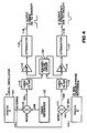
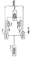
- each channel A or B has a fractional-N based local oscillator 101 or 102 which is tunable from 20 to 33 MHz which microhertz resolution.
- the respective local oscillator signals 103 and 104 are mixed with fixed 20 MHz signals 105 and 106 from a common frequency reference 107 to obtain the desired 0 to 13 MHz signals 108 and 109 by mixers 110 and 111.
- the mixer outputs 108 and 109 are respectively low pass filtered to reject the high frequency images 14 MHz and above by low pass filters 112 and 113, and then amplified by amplifiers 114 and 115.
- Step attenuators 116 and 117 are used to provide 80 dB dynamic range of output levels.
- output signals 118 and 119 are respectively independent to provide variable frequency, spectrally pure signals from 0 to 13 MHz with sufficient gains as two separate synthesizers.
- the signal synthesizer system in two phase mode is also shown as a system configuration.
- the A channel consists of the local oscillator 101, the frequency reference 107, the mixer 10, the low pass filter 112, the amplifier 114, and the attenuator 116 is configured exactly as in two channel mode shown in Figure 1.
- the reference 107 and the local oscillator signal 103 are switched before the mixer 111 by a common controller such that the A fractional-N base local oscillator is the local oscillator for the B channel as well, and the B fractional-N base local oscillator is set to 20 MHz and is used as a reference whose phase can be precisely changed relative to the fixed reference 107.
- the fixed reference 107 is used for the A channel.
- the signal synthesizer system in two tone mode is also shown as a system configuration.
- the local oscillator and reference switching is identical to the two phase mode shown in Figure 2.
- the B fractional-N base local oscillator 102 is used as a reference for the B channel.
- the B local oscillator 102 is set to a frequency at 20 MHz plus some offset which is less than 100 KHz. This results in signals at the outputs 118 and 119 of the channels A and B which are offset in frequency by up to 100 KHz.
- An important benefit of this configuration is that as the A channel changes in frequency, the B channel automatically tracks while maintaining the precise frequency offset relative to the A channel.
- the channels A and B can be combined on single output 121 by a combiner 120. Hence, different output frequencies are available from each channel. This leads the system to an another particular contribution that the use of the B oscillator 102 as a variable frequency reference allows the B channel frequency to maintain a precise frequency offset from the A channel with minimal phase noise between the channels A and B. Also this precision offset is maintained during a sweep of the A channel.
- the signal synthesizer system in pulse mode is also shown as a system configuration.
- the local oscillators 101 and 102, and the frequency reference 107 are switched exactly as in the two phase mode as shown in Figure 2 by the common controller.
- the distinction in Figure 4 is that before the output amplifiers 114 and 115, the sinewave signals 108 and 109 low pass filtered by the filters 112 and 113 are switched to a square/pulse circuit 122 which squares up and combines the signals in such a fashion as to yield a pulse waveform.
- the duty cycle reflects the phase difference between the A and B channels.
- the duty cycle is adjustable from 5% to 95%. This waveform is output on the A channel. For convenience, the complement of this waveform is available on the B channel.
- the signal outputs 118 and 119 are variable duty cycle square waves and are complementary to each other.
- the sweep capability of the fractional-N oscillators can be used.
- Arbitrary start and stop frequencies and sweep times can be specified.
- Sweeps are phase continuous. Means are provided for starting the sweep from an external trigger with minimum delay.
- Either square waves or sinewaves may be selected on each channel.
- the edges on the square wave coincide with the zero crossings of the sinewave.
- the outputs can be configured to generate only the DC offset level.
- either of the outputs can be turned off entirely via a relay. Regardless of the function selected, a nominal 50 ohm source impedance is seen, unless the high voltage option is enabled in which case a low impedance which is less than 2 ohms is seen.
- Amplitude can be controlled over a range from +23.97 dBm into 50 ohms, which is 10 volts peak to peak, to -56 dBm, which is 1 millivolt peak to peak.
- the combination of a selectable 10 dB attenuator before the output amplifier and a 0 dB to 70 dB step attenuator following the output amplifier allows the amplitude to be changed in 10 dB increments.
- the fine adjustment between 10 dB increments is provided by modulating the level of the 20 MHz reference signal before it gets into each mixer.
- a DC offset can be added on top of the AC signal from each channel. Normally, this offset is injected before the output amplifier, so its maximum level is determined by the level of the AC signal. The instantaneous maximum level of DC plus AC cannot exceed the ⁇ 5 volt limits of the output amplifier. Also, the DC signal is attenuated right along with the AC as it passes through the output attenuator. If the high voltage option is selected, the DC offset is injected right at the high voltage amplifier so a large DC offset can be obtained, even if the AC signal level is highly attenuated.
- the B channel output may be switched internally to become the level control for the A channel reference, thus allowing internal amplitude modulation on the A channel, or it can be switched into the phase control circuit of the A channel fractional-N oscillator, allowing internal phase modulation of the A channel. While internal modulation is enabled, the B channel output is disabled. Similarly, either channel A or B can be amplitude modulated, phase modulated, or both simultaneously from separate external inputs.
- the outputs of the A and B channels can be as combined together into one output by enabling the internal combiner 120 as explained in Figure 3. Since this is a broad-band resistive combiner, the level of each signal drops to one-half.
- the outputs of both channels A and B can be switched onto the calibrator circuit which is able to measure the amplitudes of either channel and relative phase between the two. Measurements taken are interpreted by the controller which in turn adjusts the level control or the fractional-N phase to correct for any error.
- the signals are switched off at the outputs of the instrument.
- An alternate configuration provided is to measure the signals present on the rear panel "external cal" inputs. This allows “remote sensing" for phase cal which lets the user eliminate the effects of loss and phase shift in his cabling to the device under test.
- the calibrator During either internal and external cal, the calibrator always measures phase of the "B" signal relative to "A” signal. The embodiment of this calibration system will be more precisely explained hereafter.
- An oven-stabilized 10 MHz frequency reference option can be installed in the instrument.
- the output of the oven goes directly to the rear panel and must be jumped across to the "external reference" input when it is used.
- An optional high voltage amplifier can be added to each channel. This amplifier following the attenuator gives four times the normal 50 ohm terminated level which is two times the normal open circuit level over a 0 Hz to 130 KHz range. The low impedance output of the high voltage amplifier is seen directly without any series backmatching resistance.
- the DC offset is injected into the input of the high voltage amplifier instead of before the output amplifier. This allows a large DC offset to be provided with a small AC signal which has come through the output attenuator.
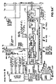
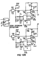
- a linear power supply 201 having seven separate outputs is provided as shown in Figure 5A. Plus and minus fifteen volt supplies are used throughout the instrument. In addition, three separate five volt supplies are available. The main five volt supply is a highly regulated and very clean supply. It is used by most of the circuit assemblies wherever the demand is fairly constant or special isolation is not required. A separate five volt supply is necessary for the keyboard assembly 202 to keep the display scan frequency components out of the main five volt supply. The third five volt supply is used to power the interface support circuitry 203 which is IEEE standard 488 interface. Finally, a +28 and -28 supply provide power for the high voltage option.
- the instrument enclosure is, of course, tied to earth ground via the line cord.
- the interface 203 ground is tied to the enclosure at a single point very close to the interface connector.
- the instrument ground is separate from earth ground. This includes all of the internal card nests, motherboard, cables, etc. RF path are provided from instrument ground to earth ground via multiple capacitors and a varistor ensures that no more than 50 volts potential appears between the two grounds.
- controller all functions of the instrument are controlled by the 6809 microprocessor on the controller board 204, operating from 56 Kbytes of ROM.
- the controller 204 accepts commands in the form of keyboard entry or via the interface and controls each of the hardware assemblies via the instrument bus.
- the instrument bus is buffered and disabled any time that instructions are not actually being written to hardware to keep processor clock frequency from coupling to sensitive circuits.
- the keyboard assembly 202 includes all switches and lights to interface with the operator. This includes 43 pushbutton switches, one rotary pulse generator (RPG), 49 individual LED's, 11 seven-segment digit displays, and 1 four-character alphanumeric display.
- the keyboard 202 is interfaced to the controller 204 via a bit-serial interface.
- the keyboard 202 holds the synchronous circuit to keep it isolated from the clean output signals.
- oven reference 205 option 1 provided for an overstabilized crystal reference 205 which is mounted below the power supply in the rear of the instrument 205.
- the output goes directly to the rear panel.
- To use the reference 205 it must be externally connected to the external reference input on the rear panel.
- the reference board generates all frequency references and clocks for the instrument. These include:
- One input is available on the rear panel which accepts an external reference signal. If this signal is at a sub-harmonic of 10 MHz, the reference will synchronize with it.
- the A and B local oscillators 101 and 102 are identical fractional-N based synthesized oscillators.
- the five separate printed circuit assemblies make up each local oscillator (LO).
- LO local oscillator
- Each fractional-N oscillator is controllable via the instrument bus over a frequency range of 19.9 MHz to 33.0 MHz with one microhertz resolution. Both fractional-N oscillators can be adjusted for phase by incrementing or decrementing in as little as 0.001 degree steps.
- the fractional-N circuits do not remember where they have been programmed in the past, so any absolute phase reference must be remembered in the controller memory after performing a phase calibration by using the calibrator assembly.
- Either fractional-N oscillator can be swept over any frequency in the 19.9 to 33.0 MHz range, either up or down, maintaining phase continuity during the sweep. Start and stop frequencies are settable to one microhertz resolution. During sweep, a "sweep limit flag" is available which signals when the fractional-N oscillator has passed a preprogrammed frequency within the frequency limits of the sweep.
- One output from the A LO 101 is permanently input to the A mixer LO port 206.
- the other A LO signal is input to the RF switch 207 where it is switched onto the B mixer LO port 208 for all operating modes other than two-channel.
- One B LO signals goes to the RF switch 207 where it is switched onto either the LO port of the B mixer 208 in case of the two channel mode, or onto the reference port of the B mixer 208 in case of the other three modes.
- the second B LO signal is made available as a 20 to 33 MHz output on the rear panel.
- the level/AM control assembly provides an audio frequency signal which either drives the A or B modulator 210 or 211 for sine operation, or drives the square wave circuit 212 for square or pulse operation. If no amplitude modulation signal is present, the output is a DC voltage proportional to the digital to analog converter (DAC) setting programmed by the controller 204. Separate digital to analog converters are provided for each of the two level outputs. If a modulation signal is persent, either internally from the channel B output, or externally from the rear panel inputs, the level outputs are proportional to both the DAC setting and the level of the modulating signal, subject to the 150 KHz bandwidth limit of the level control.
- DAC digital to analog converter
- Programmable switches are provided to allow the controller 204 to specifiy either internal or external modulation for each level control, and to direct the output of each level control to either the sinewave modulator 210 or 211 or square wave circuit 212 of the respective A and B channels.
- the modulator circuits 210 and 211 for each channel controls the level of the reference signal to the respective mixers 206 and 208 over a ten decibel range, thus controlling the level of the output signals from the instrument.
- Inputs to the A modulator 210 are the 20 MHz reference from the reference board 107 and the A level control signal from the level/AM board 209.
- the resulting level-controlled reference is band-pass filtered to eliminate harmonics of 20 MHz and limit noise outside a ⁇ 100 KHz bandwidth around 20 MHz.
- the resulting "AMPOUT" output is input to the A mixer 206.
- the modulator 211 operates in exactly the same fashion, except its 20 MHz input comes from the RF siwtch circuit 207.
- the A and B channels use identical double-balanced, active mixers to heterodyne the 20 to 33 MHz (nominal) LO signal with the 20 MHz (nominal) reference signal to generate suppressed-reference double side-band products.
- the high sideband (40 to 53 MHz) as well as the residual 20 MHz reference signals are filtered out, yielding a "pure" signal of interest between 0 and 13 MHz with all other spurious and harmonic signals suppressed.
- the lowpass filter is split between the mixer board and the pre-amp to minimize the effect of interference along the interconnect path.
- the active mixer design is optimized for low spurious and harmonic distortion.
- the pre-amplifier circuit 213 or 214 contains the latter half of the first low-pass filter for each channel.
- the signal After filtering, the signal is amplified by a fixed gain (X10) amplifier; then it goes through an additional low pass filter before being passed on.
- X10 fixed gain
- the output of the pre-amp is directed either directly to the output amplifier input, or to the square wave circuit using a controller programmed relay.
- the square wave circuit 212 has two functions. First, with the square wave function selected for either channel, that channel's signal is directed through the square circuit, which generates a crisp square wave output whose edges match the zero-crossings of the output of the pre-amp and whose amplitude is controlled by the level control from the level/ AM circuit 209. Either A or B or both may have square function selected.
- the A output of the square wave circuit is a pulse waveforms whose pulse width reflects the phase difference between the A and B pre-amp outputs.
- the B output of the square circuit 212 is the logical complement of the A waveform.
- the offset control circuit 215 generates a separate DC offset for each channel as determined by DAC's under processor control. Under normal operation, the offset signal is injected into the output amplifier summing node. If the high voltage option is enabled, the signal is injected into the summing node of the high voltage amplifier 218 or 219. A relay on the offset board directs it to one node or the other. Both channels have identical offset operation.
- the output amplifier 216 or 217 boost the signal to its maximum level of up to ⁇ 5 volts into 50 ohms ⁇ 10 volts open circuit).
- the AC circuit path from the pre-amplifier 213 or 214 can be switched through a 10 dB attenuator 220 or 221.
- this 10 dB pad is the first pad thrown in as amplitude is reduced.
- the benefits of having this first 10 dB before the amplifier include:
- the signal goes through an overload current sense circuit, and a 50 ohm backmatch resistor.
- the step attenuator 222 or 223 allows the amplitude of the output signal to be attenuated in 10 dB steps to as much as 70 dB, maintaining 50 ohm impedance throughout.
- this printed circuit board contains additional overload sensing and a cutout relay for the overloads.
- a relay is provided to divert the signal from the attenuator input to the calibrator board.
- Another relay re-directs the signal out of the attenuator 222 or 223 through the high voltage amplifier and back, when the option is selected.
- both the A and B signals are input to a summing network 224 on the A attenuator 225.
- the combined signal is output on the A channel, and the B output is terminated with 50 ohms to ground.
- This network on A is the only distinction between the A and B attenuator circuits 225 and 226.
- synchronous circuit (SYNC) 227 a small circuit which resides on the keyboard assembly taps off the output signal from the output amplifier 216 and generates a square wave whose edges are coincident with the zero-crossings of the waveform out of the amplifier. Because there may be some DC offset programmed, the SYNC circuit 227 also resquires a sample of the DC offset level to correct for this. The SYNC circuit 227 is available directly on the front panel after going through some protective circuitry.
- the final block in the instrument signal chain is the calibration 228 which is capable of measuring DC offset, and peak-to- peak amplitude on both A and B channels and can measure phase between the channels very precisely.
- the calibrator takes data points, swapping back and forth between channels and alternately engaging or disengaging the 10 dB pad 220 or 221 on the output amplifier 216 or 217 while changing the levels of the modulators 210 and 211.
- the combinations of measurements made allows most systematic errors to be corrected for yielding very precise phase comparison between A and B.
- the controller 204 iteratively changes the amplitude or phase parameter being calibrated to minimize error.
- phase calibration the controller "bumps" the phase of the fractional-N oscillator.
- amplitude calibration the controller changes the DAC settings on the level control circuit.
- offset calibration the controller changes the DAC settings on the offset control.
- the signals present at the two rear panel calibration inputs are assumed to be the A and B signals measured at the end of a cable, or after being modified by some device under test.
- the calibration process is the same as with internal calibration.
- the A calibration input is expected to be a signal from another source, and the B input is expected to be the A output of the system.
- the phase of A is bumped to align the A channel with the output of the other source.
- the other source must have its reference locked with the system in order to get a successful phase calibration.
- phase calibration system has an unique contribution to the signal synthesizer system such that with two channels in one instrument and the addition of the phase calibrator, very precise phase accuracy can be maintained.
- This phase calibration technique allows theoretically zero phase error for equal level sines, and utilizes a unique attenuator switching technique to characterize and correct for phase errors introduced by the difference between levels in the two channels.
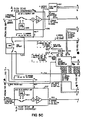
- phase calibration system as a subsystem of the signal synthesizer system is shown in a basically simplified system block diagram.
- the frequency reference 107 is connected to two sources 301 and 302 which are already discussed hereinabove as the A and B channels in Figure 1 through Figure 5.
- the two sources 301 and 302 are programmable in frequency, amplitude, and phase, by the controller 204, and are phase locked to the frequency reference 107 as explained above.
- Both outputs of the sources 301 and 302 are fed to inputs of a phase detector circuit 303 which gives an indication of when the phase between its inputs is 180 degrees.
- This phase detector circuit 303 consists of the decoder/calibrator 228 shown in Figure 5C.
- basic calibration scheme of the phase detector circuit 303 is as follows.
- the sources 301 and 302 are set up for frequency in which both sources are identical, as well as for amplitude.
- the phase of one source 301 and 302 is varied until the phase detector circuit 303 indicates 18 degrees by a signal 304.
- this point is defined as a 180 phase, and the desired phase offset is entered onto the sources 301 and 302 by the controller 204. Therefore, it is assumed that the phase of the sources 301 and 302 can be incremented very accurately, so that an accurate calibration to zero degrees will provide calibrated outputs from zero to 360 degrees.
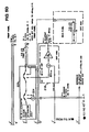
- phase detector circuit 303 of Figure 6 is described as a block diagram.
- the phase detector circuit 303 consists of five blocks which are a relay 310 to reverse inputs, two zero crossing detectors 311 and 312, a flip-flop phase detector 313, a low pass filter 314, and a comparator 315. Each function of this block diagram will be clearly explained in the following description.
- Function of the zero crossing detector 311 or 312 is to take an analog waveform and convert it to a digital waveform, transitions of which reflect the timing of the analog zero crossings.
- the zero crossing detectors 311 and 312 are optimized for speed, insensitivity to amplitude and DC offset of the input signals, as well as noise rejection. It is preferable to use integrated circuit comparators as a choice of design for the zero crossing detectors 311 and 312 which require very high speed, high gain, and low offset voltage at a good price/performance ratio.
- the zero crossing detectors 311 and 312 are precisely shown as a circuit diagram.
- the input signals Vin are capacitively coupled through a capacitor C i , to reject DC components, resis- tively divided through resistors R, and R 2 , and connected to a non-inverting input 411 of a comparator 412.
- Two feedback paths which are AC and DC feedback, are connected from comparator outputs 413 and 414 to its inputs 411 and 415.
- the AC feedback is differential, and consists of capacitors C 2 and C 3 . As the input signal 411 crosses the comparator threshold, the outputs 413 and 414 change state, and couple a signal back to the inputs 411 and 415 in a regenerative manner.
- the DC feedback path operates on the inverting input only, and consists of resistors R 3 and R 4 , and diodes D" D 2 and D 3 .
- the inverting output 414 When the input signal 411 is below the comparator threshold, the inverting output 414 is high, which forward biases the diodes D 2 and D 3 , and reverse biases the diode D l . Therefore, the inverting input 415 will be at ground potential. This sets the switching threshold to zero volts for signals crossing in the positive direction.
- the inverting output 414 goes down, which turns off the diodes D 2 and D 3 , and allows the diode D, to become forward biased.
- the voltage at the inverting input 415 now is set by voltage division between the resistor R 3 , the diode D l , and the resistor R 4 . This is then the threshold for signals crossing in the negative direction, which is designated to set to -50 mV.
- phase detector 313 In referring to the timing chart of Figure 9, the function of the phase detector 313 will be explained. Namely, two interconnected flip-flops form the phase detector 313, which is driven by the outputs of the two zero crossing detectors 311 and 312. An output Q and its complement Q of the phase detector 313 are both used by the following circuitry.
- One zero crossing detector 312 acts to set the phase detector 313, while the other zero crossing detector 311 acts to reset the phase detector 313.
- the outputs Q and Q of the phase detector 313 are then squarewaves whose duty cycle is determined by timing of the set and reset inputs S and R, which ultimately reflect the phase between the two original input signals A and B. An input phase difference of 180 degrees will produce a 50% duty cycle phase detector output.
- the timing chart shows these signals A and B for an arbitrary input phase; in this case the input B leads the input A by 90 degrees.
- a negative hysteresis voltage V, of the zerocrossing detector 311 or 312 is shown much exaggerated for the clarity of this discussion.
- this phase detector 313 preferably dictates the use of a dual Schottky TTL flip-flop for the design.
- both of the low pass filter 314 and the comparator 315 are functionally discussed in greater detail hereinbelow.
- the low pass filter 314 and the comparator 315 actually consist of two circuits respectively as shown in Figure 12A-C which shows the detailed circuit configuration of the calibration system for the design.
- the filter 314 and the comparator 315 signal the controller 214 when the phase of the input signals A and B passes through 180 degrees.
- the two filters and the two comparators are respectively identical except filter cutoff frequency.
- the low path filter 314 acts differentially on the true output Q and the complement output Q of the phase detector 313, removing their AC components and presenting their DC components to the input of the comparator 315.
- the true output Q of the phase detector 313 will vary from 0% duty cycle to 100%, hence its DC component will vary the TTL output level from low to high.
- the complement output Q will vary in the opposite manner for the same input phase change that the complement output Q will vary from 100% duty cycle to 0%, and that its DC component will vary the TTL output level from high to low.
- the two DC components will then cross each other when the input signal passes through 180 degrees, and the comparator output will change state, signalling the controller 204.
- the high gain of the comparator 315 enhances the resolution of the entire phase detection scheme, as the volts/degree at the phase detector output is rather small, i.e., 3.6 volts per 360 degrees or 10 mV per degree. This figure is closer to 500 volts/degree at the comparator output.
- the calibration system of the invention allows the controller based on a microprocessor to perform phase calibration and to measure and correct for the instrument's phase vs. amplitude chracteris- tic.
- the input reversing relay 310 is used to allow phase calibrations with the phase detector 313 hooked up normally or with its inputs reversed.
- phase detector circuit 303 indicates that the phase of the channel A with respect to the channel B is 180 degrees.
- real phase detector circuits are far from ideal in that errors will be introduced due to propagation delays, comparator offset voltages, electrical crosstalk, and many other factors as discussed as the systematic errors.
- the phase calibration system is designed to be as precise as possible, this result can be off by as much as several tenths of degrees at low frequencies, and as much as several tens of degrees at high frequencies.
- phase detector need not be accurate as the desired phase results, but it merely needs to have very good resolution and be repeatable in the short term.
- signals of differing amplitude can be phase calibrated, and correction factors are calculated from the known offset voltages.
Landscapes
- Stabilization Of Oscillater, Synchronisation, Frequency Synthesizers (AREA)
Claims (10)
Applications Claiming Priority (4)
| Application Number | Priority Date | Filing Date | Title |
|---|---|---|---|
| US06/635,312 US4630217A (en) | 1984-07-26 | 1984-07-26 | Signal synthesizer system |
| US635312 | 1984-07-26 | ||
| US06/635,949 US4648060A (en) | 1984-07-30 | 1984-07-30 | Dual channel frequency synthesizer system |
| US635949 | 1984-07-30 |
Publications (2)
| Publication Number | Publication Date |
|---|---|
| EP0172425A1 EP0172425A1 (fr) | 1986-02-26 |
| EP0172425B1 true EP0172425B1 (fr) | 1990-09-12 |
Family
ID=27092349
Family Applications (1)
| Application Number | Title | Priority Date | Filing Date |
|---|---|---|---|
| EP19850109137 Expired EP0172425B1 (fr) | 1984-07-26 | 1985-07-22 | Circuit synthétiseur de fréquence |
Country Status (2)
| Country | Link |
|---|---|
| EP (1) | EP0172425B1 (fr) |
| DE (1) | DE3579649D1 (fr) |
Families Citing this family (5)
| Publication number | Priority date | Publication date | Assignee | Title |
|---|---|---|---|---|
| GB2228840B (en) * | 1989-03-04 | 1993-02-10 | Racal Dana Instr Ltd | Frequency synthesisers |
| SE503069C2 (sv) * | 1994-07-06 | 1996-03-18 | Ericsson Telefon Ab L M | Förfarande och anordning för att fasvrida en signal |
| US6625435B1 (en) * | 2000-02-29 | 2003-09-23 | Ericsson Inc. | Frequency synthesis using a programmable offset synthesizer |
| RU2255413C1 (ru) * | 2003-12-02 | 2005-06-27 | Открытое акционерное общество "Научно-производственное объединение "Алмаз" имени академика А.А. Расплетина" | Многоканальный синтезатор сетки частот |
| CN115712080A (zh) * | 2022-11-14 | 2023-02-24 | 国网湖北省电力有限公司超高压公司 | 一种基于现场可编程门阵列的复合绝缘子核磁共振谱仪 |
Family Cites Families (4)
| Publication number | Priority date | Publication date | Assignee | Title |
|---|---|---|---|---|
| US2920284A (en) * | 1955-01-10 | 1960-01-05 | North American Aviation Inc | Signal generator having independent output frequency and phase adjustment means |
| US2864956A (en) * | 1957-12-17 | 1958-12-16 | Ca Nat Research Council | Stabilization system for tunable oscillator with reference to a pair of stable oscillators |
| US3854102A (en) * | 1973-08-09 | 1974-12-10 | Itt | Multiple frequency band frequency synthesizer |
| DE2828224A1 (de) * | 1978-06-28 | 1980-01-10 | Licentia Gmbh | Frequenzveraenderlicher schwingungserzeuger |
-
1985
- 1985-07-22 EP EP19850109137 patent/EP0172425B1/fr not_active Expired
- 1985-07-22 DE DE8585109137T patent/DE3579649D1/de not_active Expired - Lifetime
Also Published As
| Publication number | Publication date |
|---|---|
| DE3579649D1 (de) | 1990-10-18 |
| EP0172425A1 (fr) | 1986-02-26 |
Similar Documents
| Publication | Publication Date | Title |
|---|---|---|
| US4648060A (en) | Dual channel frequency synthesizer system | |
| CN100472941C (zh) | 正交调制器及其校准方法 | |
| US4630217A (en) | Signal synthesizer system | |
| US5952834A (en) | Low noise signal synthesizer and phase noise measurement system | |
| CN106257300B (zh) | 一种测试和测量仪器和用于确定补偿值的方法 | |
| US6480006B1 (en) | Method for measuring phase noise using a low noise synthesizer | |
| JPH01221904A (ja) | 位相同期ループ周波数シンセサイザ | |
| US11041884B2 (en) | Calibration for test and measurement instrument including asynchronous time-interleaved digitizer using harmonic mixing | |
| US5631553A (en) | High precision RF vector analysis system based on synchronous sampling | |
| EP0172425B1 (fr) | Circuit synthétiseur de fréquence | |
| US4149122A (en) | Wideband tracking generator for harmonic mixing receivers | |
| US6731917B1 (en) | Method and apparatus for minimizing image power in the output of a receiver circuit | |
| US4138645A (en) | Wideband signal calibration system | |
| US5974362A (en) | Signal generator for testing radio frequency components | |
| JPS58174861A (ja) | アナログ・デジタル変換器の特性測定装置 | |
| EP0420082A2 (fr) | Source de signal de balayage synchronisée numériquement | |
| US5023571A (en) | Digitally-synchronized sweep signal source | |
| JP3594812B2 (ja) | 信号受信装置 | |
| US4138646A (en) | Wideband absolute calibration system | |
| JP2000329806A (ja) | スペクトラムアナライザ | |
| SU1365059A1 (ru) | Широкополосна многозначна мера переменного напр жени | |
| Brindley | Modern electronic test equipment | |
| JP3096365B2 (ja) | Dtmf信号生成回路 | |
| SU1767453A1 (ru) | Калибратор амплитудной модул ции | |
| Instone | Advances in microwave measurements |
Legal Events
| Date | Code | Title | Description |
|---|---|---|---|
| PUAI | Public reference made under article 153(3) epc to a published international application that has entered the european phase |
Free format text: ORIGINAL CODE: 0009012 |
|
| AK | Designated contracting states |
Designated state(s): DE FR GB |
|
| 17P | Request for examination filed |
Effective date: 19860812 |
|
| 17Q | First examination report despatched |
Effective date: 19880906 |
|
| GRAA | (expected) grant |
Free format text: ORIGINAL CODE: 0009210 |
|
| AK | Designated contracting states |
Kind code of ref document: B1 Designated state(s): DE FR GB |
|
| REF | Corresponds to: |
Ref document number: 3579649 Country of ref document: DE Date of ref document: 19901018 |
|
| ET | Fr: translation filed | ||
| PLBE | No opposition filed within time limit |
Free format text: ORIGINAL CODE: 0009261 |
|
| STAA | Information on the status of an ep patent application or granted ep patent |
Free format text: STATUS: NO OPPOSITION FILED WITHIN TIME LIMIT |
|
| 26N | No opposition filed | ||
| PGFP | Annual fee paid to national office [announced via postgrant information from national office to epo] |
Ref country code: FR Payment date: 19930610 Year of fee payment: 9 |
|
| PGFP | Annual fee paid to national office [announced via postgrant information from national office to epo] |
Ref country code: DE Payment date: 19930618 Year of fee payment: 9 |
|
| PGFP | Annual fee paid to national office [announced via postgrant information from national office to epo] |
Ref country code: GB Payment date: 19930624 Year of fee payment: 9 |
|
| PG25 | Lapsed in a contracting state [announced via postgrant information from national office to epo] |
Ref country code: GB Effective date: 19940722 |
|
| GBPC | Gb: european patent ceased through non-payment of renewal fee |
Effective date: 19940722 |
|
| PG25 | Lapsed in a contracting state [announced via postgrant information from national office to epo] |
Ref country code: FR Effective date: 19950331 |
|
| PG25 | Lapsed in a contracting state [announced via postgrant information from national office to epo] |
Ref country code: DE Effective date: 19950401 |
|
| REG | Reference to a national code |
Ref country code: FR Ref legal event code: ST |