EP0171141B1 - Cash register and method of modifying programmes stored in said cash register - Google Patents
Cash register and method of modifying programmes stored in said cash register Download PDFInfo
- Publication number
- EP0171141B1 EP0171141B1 EP85303499A EP85303499A EP0171141B1 EP 0171141 B1 EP0171141 B1 EP 0171141B1 EP 85303499 A EP85303499 A EP 85303499A EP 85303499 A EP85303499 A EP 85303499A EP 0171141 B1 EP0171141 B1 EP 0171141B1
- Authority
- EP
- European Patent Office
- Prior art keywords
- programs
- memory
- memory means
- modified
- data
- Prior art date
- Legal status (The legal status is an assumption and is not a legal conclusion. Google has not performed a legal analysis and makes no representation as to the accuracy of the status listed.)
- Expired
Links
Images

Classifications
-
- G—PHYSICS
- G06—COMPUTING OR CALCULATING; COUNTING
- G06Q—INFORMATION AND COMMUNICATION TECHNOLOGY [ICT] SPECIALLY ADAPTED FOR ADMINISTRATIVE, COMMERCIAL, FINANCIAL, MANAGERIAL OR SUPERVISORY PURPOSES; SYSTEMS OR METHODS SPECIALLY ADAPTED FOR ADMINISTRATIVE, COMMERCIAL, FINANCIAL, MANAGERIAL OR SUPERVISORY PURPOSES, NOT OTHERWISE PROVIDED FOR
- G06Q30/00—Commerce
- G06Q30/04—Billing or invoicing
-
- G—PHYSICS
- G07—CHECKING-DEVICES
- G07G—REGISTERING THE RECEIPT OF CASH, VALUABLES, OR TOKENS
- G07G1/00—Cash registers
- G07G1/12—Cash registers electronically operated
Definitions
- the present invention relates to an electronic apparatus, such as an electronic cash register (hereinafter called ECR) that registers and processes a variety of trade data, or a "teller machine" normally used to process bank data.
- ECR electronic cash register
- the present invention relates more particularly to a method of modifying programs stored in an ECR.
- the system simply and easily implements required changes or modifications of programs related to the processing of a variety of trade data stored in a stationary memory.
- a low cost stationary mask ROM read-only memory
- the programs are unalterable once they have been written into the mask ROM.
- the inventors proposed a method of writing and storing a variety of specific data needed to modify programs stored in an ECR's mask ROM by using the following memory means: a second memory containing addresses identical to those in the mask ROM which serves primarily as the first memory; a third memory storing the data denoting addresses of the programs that require modification; a fourth memory storing modified programs; and a means for entering and processing a variety of trade data using the ECR's mode-select means of selecting a specific mode, without providing the means of writing programs independent of the ECR.
- the proposed system still had the disadvantages of requiring independent storage of data in the third and fourth memories and it involved complex operations for writing data including the data for the modified programs.
- the present invention aims at providing a new system which facilitates inputting of modified programs in electronic cash registers.
- an electronic cash register for registering and processing a variety of trading data an electronic cash register for registering and processing a variety of trading data comprising:
- electronic data processing apparatus having a first memory means which is a fixed memory means and in which programs for the operation of the apparatus are stored, and means to allow the apparatus to follow modified versions of the said progams comprising:
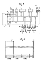
- Reference number 1 indicates the central processing unit (CPU) which is connected to the following device via data bus 13 and address bus 14, respectively.
- These devices include the first memory (mask ROM) 2 which permanently stores the various programs needed for processing trading data and for setting modified programs; the second memory (RAM) 3 which contains addresses identical to those of mask ROM 2 and stores such data, indicating against the address positions of mask ROM 2 whether or not the required program has already been modified; the third memory (RAM) 4 which stores the addresses of the modified program of mask ROM 2 and the next address of the same modified program, bank data denoting the data area storing the modified program, and the modified program itself; means (RAM) 6 for storing the registered and processed data; input means 7 for inputting a variety of trading data and selecting any of the mode data denoting registration, inspection, and precise calculation of accounts; display means 9 for displaying input/output data; printer means 8 for printing the input/output data onto receipts; and a drawer 10 that stores cash coming from registered transactions.
- first memory mask ROM
- RAM random access
- Reference number 11 indicates the decoder that decodes the address on the address bus 14 in order to select any of the component elements described above.
- Reference number 12 indicates a flip flop unit, which is activated by signal "1" from RAM 3 and outputs an interruption signal to the CPU 1 on a signal from the activated flip flop 12. Also, in response to the final step of the modified program stored in RAM 4, the activated flip flop 12 detects the position of a modified address in a reset program by a signal from the CPU 1.
- Reference number 15 indicates the key interface (key I/F), 16 the printer interface (P I/F), 17 the display interface (D I/F) and 18 the input interface (I/O I/F), respectively.
- the first memory mask ROM 2 related to the preferred embodiment of the present invention stores programs available for setting modified programs in area "a".
- Input means 7 is provided with a group of- function keys F including the mode selector M, the designated key "A" and a group of digital keys N.
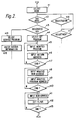
- the operator After selectively designating the required program by operating both the digital keys N and the function keys F, the operator then causes the third memory ROM 4 to store the required program (step n5).
- the third memory ROM 4 stores the required program (step n5).
- both the digital and function keys of input means 7 can be made available for designating specific commands for setting the desired programs. Since these keys can be operated in the same manner as any conventional computer capable of entering programs, explanations regarding them are omitted.
- the starting address of the modified program is first written into the designated position of the third memory RAM 4, and then sequentially written into the third memory RAM 4 are: address A of the program stored in the first memory mask ROM 2 and requiring change; the data of the memory bank storing the modified program of address A; the address of the program following the modified program stored in the first memory mask ROM 2; and the modified program in address A of the mask ROM 2.
- a command for executing a jump to the return address destined for the first memory mask ROM 2 is written into the third memory RAM 4.
- the operator sets flags into the second memory RAM 3 indicating the changes in the programs stored in the first memory ROM 2 (steps n11 through n13).
- the operator operates the mode selector M for- setting the desired position, for example, into the registration mode or the precise calculation mode, before executing the process program of the first memory mask ROM 2.
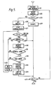
- the procedure needed for executing programs stored in the first memory mask ROM 2 is described below.
- the CPU 1 sequentially addresses the first memory mask ROM 2 (steps n21 and n22).
- programs stored in the first memory mask ROM 2 are sequentially accessed before the required program is eventually executed (step n24).
- the second memory RAM 3 is also addressed, as was done against the first memory mask ROM 2, and receives the address data from the CPU 1, the second memory RAM 3 is addressed synchronous with the first memory mask ROM 2, thus making it possible to read the address position correctly.
- the second memory RAM 3 stores code "0" while executing those program steps requiring no change or modification and code "1" while program steps requiring any change or modification are underway. While the second memory RAM 3 continues to output code "0", flip flop 12 remains reset, and, as a result, the CPU 1 causes the first memory mask ROM 2 to sequentially proceed through the program steps before the interruption signal from flip flop 12 arrives. When the address position of the first memory mask ROM 2 reaches the address position A at which the program should be changed, the second memory RAM 3 then outputs flag signal "1" so that flip flop 12 can be activated.
- flip flop 12 detects that the address position requiring the change of program has been reached by identifying the flag contents stored in the second memory RAM 3 (step n23), and, as a result, flip flop 12 outputs an interruption signal to the CPU 1 to execute an interruption (step n26).
- the CPU 1 identifies whether the data is FFFFH or not (step n28) by referring to the starting address of the third memory RAM 4 (step n27). If the data is FFFFH, the modified program is then terminated. If the data is identified as being other than FFFFH, the CPU 1 then identifies whether the data is OOOOH or not (step n29).
- step n28 the CPU 1 activates step n28 by referring to the next address (step n35).
- the CPU 1 temporarily memorizes the present address value A, and then, by referring to the address data stored in the third memory ROM 4, the CPU 1 detects the address position of ROM 4 that stores the modified program matching the temporarily memorized address value A (steps n30 and n31). If these addresses are different from each other, the CPU 1 then causes the operation mode to proceed to step n35. If these addresses correctly match, the CPU 1 then identifies the bank data (step n32). If the bank data are different from each other, the CPU 1 causes the operation mode to proceed to step n35. If these bank data correctly match, the CPU 1 then causes the operation mode to jump onto the position of the modified program before executing the modified program stored in address A of RAM 4 (step n33).
- the modified program stores a jump command at its final stage to cause the operation mode to again access the address value next to the changed address position of the first memory mask ROM 2.
- flip flop 12 is reset, and, at the same time, the operation mode jumps onto the first memory mask ROM 2 (step n34) so that the program of the first memory ROM 2 can be executed again.
- the CPU 1 causes the programs of the first memory mask ROM 2 to be sequentially executed.
- flip flop 12 is again activated to generate an interruption signal for delivery to the CPU 1 in order for the modified program correctly matching the address position of the third memory RAM 4 to be executed.
- the second memory RAM 3 is provided with a plurality of flags at a rate of 1 bit against 1 byte of the first memory ROM 2.
- the next address plays the role of linking data between a plurality of modified programs. Therefore, if it is necessary to add any other modified programs, these can easily be added as required by causing the operation mode to move from the starting address FFFFH to the ensuing addresses in accordance with the operation modes described above.
- the operation system described above provides the modified programs with bank data, allowing a comparison of the bank data in the running program with those bank data stored in the modified programs.
- ECR electronic cash register
- memory means for storing such data, memorizing whether any change or modification should be applied to programs in these addresses or not, memory means that stores the memory bank data memorizing addresses of the modified programs among those programs stored in the mask ROM and the modified programs themselves; and input means that inputs and processes a variety of trading data by causing the mode selector to select a specific mode without the need to use any program writer independent of the ECR.
Landscapes
- Business, Economics & Management (AREA)
- Physics & Mathematics (AREA)
- Development Economics (AREA)
- General Physics & Mathematics (AREA)
- Economics (AREA)
- Marketing (AREA)
- Strategic Management (AREA)
- Finance (AREA)
- General Business, Economics & Management (AREA)
- Accounting & Taxation (AREA)
- Engineering & Computer Science (AREA)
- Theoretical Computer Science (AREA)
- Cash Registers Or Receiving Machines (AREA)
- Record Information Processing For Printing (AREA)
Applications Claiming Priority (2)
| Application Number | Priority Date | Filing Date | Title |
|---|---|---|---|
| JP100207/84 | 1984-05-17 | ||
| JP59100207A JPS60243795A (ja) | 1984-05-17 | 1984-05-17 | 電子レジスタの変更プログラム設定装置 |
Publications (2)
| Publication Number | Publication Date |
|---|---|
| EP0171141A1 EP0171141A1 (en) | 1986-02-12 |
| EP0171141B1 true EP0171141B1 (en) | 1989-01-25 |
Family
ID=14267856
Family Applications (1)
| Application Number | Title | Priority Date | Filing Date |
|---|---|---|---|
| EP85303499A Expired EP0171141B1 (en) | 1984-05-17 | 1985-05-17 | Cash register and method of modifying programmes stored in said cash register |
Country Status (5)
| Country | Link |
|---|---|
| US (1) | US4811219A (enExample) |
| EP (1) | EP0171141B1 (enExample) |
| JP (1) | JPS60243795A (enExample) |
| CA (1) | CA1247242A (enExample) |
| DE (1) | DE3567979D1 (enExample) |
Families Citing this family (16)
| Publication number | Priority date | Publication date | Assignee | Title |
|---|---|---|---|---|
| US5549805A (en) * | 1984-03-29 | 1996-08-27 | The Board Of Regents Of The University Of Nebraska | Digital DNA typing |
| JPS6391796A (ja) * | 1986-10-06 | 1988-04-22 | シャープ株式会社 | 印字フオ−マツトの変更方式 |
| JPH01232447A (ja) * | 1988-03-11 | 1989-09-18 | Mitsubishi Electric Corp | シングル・チップ・マイクロコンピュータ |
| DE68925003T2 (de) * | 1988-07-14 | 1996-06-13 | Casio Computer Co Ltd | Belegdatenverarbeitungssystem. |
| US5369776A (en) * | 1988-07-14 | 1994-11-29 | Casio Computer Co., Ltd. | Apparatus for producing slips of variable length and having pre-stored word names, and wherein labels are added to word data thereon |
| JPH0253198A (ja) * | 1988-08-17 | 1990-02-22 | Omron Tateisi Electron Co | 取引処理装置 |
| GB2250838A (en) * | 1990-12-11 | 1992-06-17 | Honda Motor Co Ltd | Patching a program stored in ROM |
| WO1992012478A1 (en) * | 1991-01-09 | 1992-07-23 | Verifone, Inc. | Transaction automation system including novel memory architecture and management |
| US5263164A (en) | 1991-01-09 | 1993-11-16 | Verifone, Inc. | Method and structure for determining transaction system hardware and software configurations |
| JP2893989B2 (ja) * | 1991-04-05 | 1999-05-24 | 松下電器産業株式会社 | 電子レジスタ |
| US20030195846A1 (en) | 1996-06-05 | 2003-10-16 | David Felger | Method of billing a purchase made over a computer network |
| US8229844B2 (en) | 1996-06-05 | 2012-07-24 | Fraud Control Systems.Com Corporation | Method of billing a purchase made over a computer network |
| US7555458B1 (en) | 1996-06-05 | 2009-06-30 | Fraud Control System.Com Corporation | Method of billing a purchase made over a computer network |
| US6216224B1 (en) * | 1998-06-05 | 2001-04-10 | Micron Technology Inc. | Method for read only memory shadowing |
| US6330667B1 (en) | 1998-06-05 | 2001-12-11 | Micron Technology, Inc. | System for read only memory shadowing circuit for copying a quantity of rom data to the ram prior to initialization of the computer system |
| JP6601450B2 (ja) * | 2017-04-17 | 2019-11-06 | カシオ計算機株式会社 | 情報処理装置、情報更新システム及びプログラム |
Family Cites Families (13)
| Publication number | Priority date | Publication date | Assignee | Title |
|---|---|---|---|---|
| JPS52144940A (en) * | 1976-05-28 | 1977-12-02 | Tokyo Electric Co Ltd | Electronic cash register |
| DE2840982B2 (de) * | 1977-10-08 | 1980-07-03 | Tokyo Electric Co., Ltd., Tokio | Elektronische Registrierkasse mit einer Datenverarbeitungseinheit und elektronisches Registrierkassensystem |
| US4245311A (en) * | 1978-02-10 | 1981-01-13 | Casio Computer Co., Ltd. | Electronic cash register |
| JPS5582359A (en) * | 1978-12-18 | 1980-06-21 | Toshiba Corp | Microprogram test unit |
| GB2058424B (en) * | 1979-09-10 | 1983-06-08 | Casio Computer Co Ltd | Electronic cash register |
| JPS5840776B2 (ja) * | 1980-03-26 | 1983-09-07 | オムロン株式会社 | 電子式キヤツシユレジスタ |
| JPS5772301A (en) * | 1980-10-24 | 1982-05-06 | Tokyo Shibaura Electric Co | Water-cooled resistor |
| DE3175615D1 (en) * | 1980-12-24 | 1987-01-02 | Olivetti & Co Spa | Data recording machine |
| US4403303A (en) * | 1981-05-15 | 1983-09-06 | Beehive International | Terminal configuration manager |
| JPS57197642A (en) * | 1981-05-29 | 1982-12-03 | Sharp Corp | Information transmitting system |
| US4554630A (en) * | 1981-08-24 | 1985-11-19 | Genrad, Inc. | Control apparatus for back-driving computer memory and forcing execution of idle loop program in external memory |
| US4688173A (en) * | 1982-04-26 | 1987-08-18 | Sharp Kabushiki Kaisha | Program modification system in an electronic cash register |
| US4607332A (en) * | 1983-01-14 | 1986-08-19 | At&T Bell Laboratories | Dynamic alteration of firmware programs in Read-Only Memory based systems |
-
1984
- 1984-05-17 JP JP59100207A patent/JPS60243795A/ja active Granted
-
1985
- 1985-05-16 CA CA000481732A patent/CA1247242A/en not_active Expired
- 1985-05-17 EP EP85303499A patent/EP0171141B1/en not_active Expired
- 1985-05-17 DE DE8585303499T patent/DE3567979D1/de not_active Expired
-
1987
- 1987-11-03 US US07/117,907 patent/US4811219A/en not_active Expired - Fee Related
Also Published As
| Publication number | Publication date |
|---|---|
| JPS60243795A (ja) | 1985-12-03 |
| US4811219A (en) | 1989-03-07 |
| CA1247242A (en) | 1988-12-20 |
| JPS6355119B2 (enExample) | 1988-11-01 |
| EP0171141A1 (en) | 1986-02-12 |
| DE3567979D1 (en) | 1989-03-02 |
Similar Documents
| Publication | Publication Date | Title |
|---|---|---|
| EP0171141B1 (en) | Cash register and method of modifying programmes stored in said cash register | |
| US4445795A (en) | Method and apparatus for merge processing in a text processing system | |
| USRE43248E1 (en) | Interoperability with multiple instruction sets | |
| US5574269A (en) | Processing system for processing information in card having plurality of functions | |
| JPH02123468A (ja) | コンピユータ支援作図システムにおける作図方法 | |
| US4688173A (en) | Program modification system in an electronic cash register | |
| US4575816A (en) | Interactive transactions processor using sequence table pointers to access function table statements controlling execution of specific interactive functions | |
| US4408292A (en) | Data print control in an electronic cash register | |
| US4635196A (en) | Tax or exemption selecting electronic cash register | |
| US4636971A (en) | Data processing device with specifiable program order | |
| GB2128005A (en) | Key function presetting | |
| US5668936A (en) | Printer for exclusively selecting a host apparatus and a command system for use with the selected host apparatus | |
| JPS619790A (ja) | 電子式キヤツシユレジスタ | |
| US4727502A (en) | Programmable electronic calculator | |
| EP0315111B1 (en) | Data processing device | |
| US20030159023A1 (en) | Repeated instruction execution | |
| GB2075734A (en) | Voice data output apparatus | |
| US5564057A (en) | Microprocessor architecture which facilitates input/output utilizing pairs of registers which the same address | |
| US5675776A (en) | Data processor using FIFO memories for routing operations to parallel operational units | |
| JPS58186875A (ja) | 電子式キヤツシユレジスタ等のプログラム変更方式 | |
| JPS58195268A (ja) | 電子レジスタ | |
| JPH0115906B2 (enExample) | ||
| JPS59177649A (ja) | デ−タ処理装置 | |
| JPH0658711B2 (ja) | Posシステム | |
| JP2506591B2 (ja) | 補助処理装置 |
Legal Events
| Date | Code | Title | Description |
|---|---|---|---|
| PUAI | Public reference made under article 153(3) epc to a published international application that has entered the european phase |
Free format text: ORIGINAL CODE: 0009012 |
|
| AK | Designated contracting states |
Designated state(s): DE GB |
|
| 17P | Request for examination filed |
Effective date: 19860505 |
|
| 17Q | First examination report despatched |
Effective date: 19870916 |
|
| GRAA | (expected) grant |
Free format text: ORIGINAL CODE: 0009210 |
|
| AK | Designated contracting states |
Kind code of ref document: B1 Designated state(s): DE GB |
|
| REF | Corresponds to: |
Ref document number: 3567979 Country of ref document: DE Date of ref document: 19890302 |
|
| PLBE | No opposition filed within time limit |
Free format text: ORIGINAL CODE: 0009261 |
|
| STAA | Information on the status of an ep patent application or granted ep patent |
Free format text: STATUS: NO OPPOSITION FILED WITHIN TIME LIMIT |
|
| 26N | No opposition filed | ||
| PGFP | Annual fee paid to national office [announced via postgrant information from national office to epo] |
Ref country code: GB Payment date: 19980508 Year of fee payment: 14 |
|
| PGFP | Annual fee paid to national office [announced via postgrant information from national office to epo] |
Ref country code: DE Payment date: 19980522 Year of fee payment: 14 |
|
| PG25 | Lapsed in a contracting state [announced via postgrant information from national office to epo] |
Ref country code: GB Free format text: LAPSE BECAUSE OF NON-PAYMENT OF DUE FEES Effective date: 19990517 |
|
| GBPC | Gb: european patent ceased through non-payment of renewal fee |
Effective date: 19990517 |
|
| PG25 | Lapsed in a contracting state [announced via postgrant information from national office to epo] |
Ref country code: DE Free format text: LAPSE BECAUSE OF NON-PAYMENT OF DUE FEES Effective date: 20000301 |