EP0171027A2 - Optischer Sender - Google Patents
Optischer Sender Download PDFInfo
- Publication number
- EP0171027A2 EP0171027A2 EP85109595A EP85109595A EP0171027A2 EP 0171027 A2 EP0171027 A2 EP 0171027A2 EP 85109595 A EP85109595 A EP 85109595A EP 85109595 A EP85109595 A EP 85109595A EP 0171027 A2 EP0171027 A2 EP 0171027A2
- Authority
- EP
- European Patent Office
- Prior art keywords
- current
- lasing
- dfb
- threshold value
- laser
- Prior art date
- Legal status (The legal status is an assumption and is not a legal conclusion. Google has not performed a legal analysis and makes no representation as to the accuracy of the status listed.)
- Granted
Links
- 230000003287 optical effect Effects 0.000 title claims abstract description 17
- 238000002347 injection Methods 0.000 claims abstract description 19
- 239000007924 injection Substances 0.000 claims abstract description 19
- 239000004065 semiconductor Substances 0.000 claims abstract description 12
- 230000003247 decreasing effect Effects 0.000 claims abstract description 3
- 239000013307 optical fiber Substances 0.000 abstract description 13
- 238000004891 communication Methods 0.000 abstract description 8
- 238000001228 spectrum Methods 0.000 description 11
- 230000005540 biological transmission Effects 0.000 description 9
- 239000006185 dispersion Substances 0.000 description 7
- 230000008878 coupling Effects 0.000 description 5
- 238000010168 coupling process Methods 0.000 description 5
- 238000005859 coupling reaction Methods 0.000 description 5
- 230000008859 change Effects 0.000 description 3
- 239000000203 mixture Substances 0.000 description 3
- 230000010355 oscillation Effects 0.000 description 3
- 238000012360 testing method Methods 0.000 description 3
- 238000000098 azimuthal photoelectron diffraction Methods 0.000 description 2
- 239000003990 capacitor Substances 0.000 description 2
- 238000005253 cladding Methods 0.000 description 2
- 238000010586 diagram Methods 0.000 description 2
- 238000011156 evaluation Methods 0.000 description 2
- 238000004519 manufacturing process Methods 0.000 description 2
- 229910000530 Gallium indium arsenide Inorganic materials 0.000 description 1
- 230000008901 benefit Effects 0.000 description 1
- 230000000903 blocking effect Effects 0.000 description 1
- 238000010276 construction Methods 0.000 description 1
- 230000005611 electricity Effects 0.000 description 1
- 239000000835 fiber Substances 0.000 description 1
- 229910052732 germanium Inorganic materials 0.000 description 1
- GNPVGFCGXDBREM-UHFFFAOYSA-N germanium atom Chemical compound [Ge] GNPVGFCGXDBREM-UHFFFAOYSA-N 0.000 description 1
- 230000006872 improvement Effects 0.000 description 1
- 239000000463 material Substances 0.000 description 1
- 238000005259 measurement Methods 0.000 description 1
- 238000000034 method Methods 0.000 description 1
- 230000004044 response Effects 0.000 description 1
- 230000035945 sensitivity Effects 0.000 description 1
- 239000000758 substrate Substances 0.000 description 1
Images

Classifications
-
- H—ELECTRICITY
- H01—ELECTRIC ELEMENTS
- H01S—DEVICES USING THE PROCESS OF LIGHT AMPLIFICATION BY STIMULATED EMISSION OF RADIATION [LASER] TO AMPLIFY OR GENERATE LIGHT; DEVICES USING STIMULATED EMISSION OF ELECTROMAGNETIC RADIATION IN WAVE RANGES OTHER THAN OPTICAL
- H01S5/00—Semiconductor lasers
- H01S5/06—Arrangements for controlling the laser output parameters, e.g. by operating on the active medium
- H01S5/0601—Arrangements for controlling the laser output parameters, e.g. by operating on the active medium comprising an absorbing region
-
- H—ELECTRICITY
- H01—ELECTRIC ELEMENTS
- H01S—DEVICES USING THE PROCESS OF LIGHT AMPLIFICATION BY STIMULATED EMISSION OF RADIATION [LASER] TO AMPLIFY OR GENERATE LIGHT; DEVICES USING STIMULATED EMISSION OF ELECTROMAGNETIC RADIATION IN WAVE RANGES OTHER THAN OPTICAL
- H01S5/00—Semiconductor lasers
- H01S5/10—Construction or shape of the optical resonator, e.g. extended or external cavity, coupled cavities, bent-guide, varying width, thickness or composition of the active region
- H01S5/12—Construction or shape of the optical resonator, e.g. extended or external cavity, coupled cavities, bent-guide, varying width, thickness or composition of the active region the resonator having a periodic structure, e.g. in distributed feedback [DFB] lasers
-
- G—PHYSICS
- G02—OPTICS
- G02F—OPTICAL DEVICES OR ARRANGEMENTS FOR THE CONTROL OF LIGHT BY MODIFICATION OF THE OPTICAL PROPERTIES OF THE MEDIA OF THE ELEMENTS INVOLVED THEREIN; NON-LINEAR OPTICS; FREQUENCY-CHANGING OF LIGHT; OPTICAL LOGIC ELEMENTS; OPTICAL ANALOGUE/DIGITAL CONVERTERS
- G02F3/00—Optical logic elements; Optical bistable devices
- G02F3/02—Optical bistable devices
- G02F3/026—Optical bistable devices based on laser effects
-
- H—ELECTRICITY
- H01—ELECTRIC ELEMENTS
- H01S—DEVICES USING THE PROCESS OF LIGHT AMPLIFICATION BY STIMULATED EMISSION OF RADIATION [LASER] TO AMPLIFY OR GENERATE LIGHT; DEVICES USING STIMULATED EMISSION OF ELECTROMAGNETIC RADIATION IN WAVE RANGES OTHER THAN OPTICAL
- H01S5/00—Semiconductor lasers
- H01S5/06—Arrangements for controlling the laser output parameters, e.g. by operating on the active medium
- H01S5/0601—Arrangements for controlling the laser output parameters, e.g. by operating on the active medium comprising an absorbing region
- H01S5/0602—Arrangements for controlling the laser output parameters, e.g. by operating on the active medium comprising an absorbing region which is an umpumped part of the active layer
-
- H—ELECTRICITY
- H01—ELECTRIC ELEMENTS
- H01S—DEVICES USING THE PROCESS OF LIGHT AMPLIFICATION BY STIMULATED EMISSION OF RADIATION [LASER] TO AMPLIFY OR GENERATE LIGHT; DEVICES USING STIMULATED EMISSION OF ELECTROMAGNETIC RADIATION IN WAVE RANGES OTHER THAN OPTICAL
- H01S5/00—Semiconductor lasers
- H01S5/06—Arrangements for controlling the laser output parameters, e.g. by operating on the active medium
- H01S5/062—Arrangements for controlling the laser output parameters, e.g. by operating on the active medium by varying the potential of the electrodes
- H01S5/06209—Arrangements for controlling the laser output parameters, e.g. by operating on the active medium by varying the potential of the electrodes in single-section lasers
- H01S5/06216—Pulse modulation or generation
-
- H—ELECTRICITY
- H01—ELECTRIC ELEMENTS
- H01S—DEVICES USING THE PROCESS OF LIGHT AMPLIFICATION BY STIMULATED EMISSION OF RADIATION [LASER] TO AMPLIFY OR GENERATE LIGHT; DEVICES USING STIMULATED EMISSION OF ELECTROMAGNETIC RADIATION IN WAVE RANGES OTHER THAN OPTICAL
- H01S5/00—Semiconductor lasers
- H01S5/20—Structure or shape of the semiconductor body to guide the optical wave ; Confining structures perpendicular to the optical axis, e.g. index or gain guiding, stripe geometry, broad area lasers, gain tailoring, transverse or lateral reflectors, special cladding structures, MQW barrier reflection layers
- H01S5/22—Structure or shape of the semiconductor body to guide the optical wave ; Confining structures perpendicular to the optical axis, e.g. index or gain guiding, stripe geometry, broad area lasers, gain tailoring, transverse or lateral reflectors, special cladding structures, MQW barrier reflection layers having a ridge or stripe structure
- H01S5/227—Buried mesa structure ; Striped active layer
- H01S5/2275—Buried mesa structure ; Striped active layer mesa created by etching
Definitions
- the present invention relates to an optical transmitter for optical fiber communications.
- DFB LDs distributed feedback semiconductor lasers
- APDs high sensitivity light receiving elements
- optical fiber communications over a distance of more than 100 km has recently been brought to a practicable stage. Studies are presently under way for further increasing the transmission range or the transmission rate.
- wavelength dispersion of optical fibers One of major obstructions to longer range and higher rate lightwave communications is the wavelength dispersion of optical fibers. Specifically, while in the wavelength range of 1.5 - 1.6 ⁇ m the transmission loss of optical fibers is minimal and long-distance transmission is hopeful, the wavelength dispersion due mainly to material dispersion amounts to about -2 ps/km/A in that specific wavelength range., Hence, in order that transmission may be effected over a distance of the order of 100 km with a modulation rate of 2 Gb/s, a light source which naturally is operable in a single longitudinal mode is essential and, yet, the spread of its spectrum width has to be restricted to about 0.8 A.
- the carrier density of an active layer in the DFB LD is modulated and, therefore, the lasing wavelength is necessarily modulated ("wavelength chirping" as generally referred to), undesirably allowing the spectrum line width to expand to about 1-2 A.
- wavelength chirping as generally referred to
- the transmissible distance is limited by wavelength dispersion rather than by transmission loss.
- an optical transmitter including at least a bistable distributed feedback semiconductor laser having hysteresis which includes a first lasing threshold value associated with a case wherein an injection current is increased and a second lasing threshold value associated with a case wherein the injection current is decreased, a bias circuit for applying a bias current lower than the second lasing threshold value to the semiconductor laser, and a drive circuit for applying to the semiconductor laser a current pulse having a peak which is higher than the first lasing threshold value when the current pulse is superposed on the bias current.
- bistable DFB LD which constitutes an essential element of the present invention. Even with a DFB LD, a bistable mode operation is attainable by defining a non-injection region where no current is injected, as taught by Akiba et al in IEEE Journal of Quantum Electronics. Vol. QE-19, No. 6, page 1053, issued 1983.
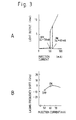
- the light output of the above- mentioned type of DFB LD showed a hysteresis characteristics responsive to injection current; the lasing threshold current I ON ,t h at the time of rise measured 60 mA and the lasing threshold current I OFF,th at the time of fall, 50 mA.
- the previously mentioned paper presented by Akiba et al teaches such a hysteresis characteristic but not a lasing spectrum and the like.
- a single mode operation with a lasing wavelength of 1,550 ⁇ m occurs in an injection current range of the order of 50 - 100 mA.
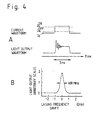
- a rectangular pulse current was applied to a bistable DFB LD having the above-described characteristic to evaluate its response.
- a dc bias current I b was set at 48 mA which was lower than I OFF,th and pulses having a peak value of 15 mA and a width of 5 ns were applied to the DFB LD.
- the resulting light output showed significant relaxation oscillation in its waveform at the time of rise.
- a semi- conductor laser under such significant relaxation oscillation shows a significant change in lasing frequency because the carrier density of its active layer is greatly modulated.
- the tested bistable DFB LD has a lasing spectrum line width of about 600 MHz in terms of half width as shown in FIG. 4B and, thus, the amount of fluctuation of lasing frequency is small.
- the reason is that, as shwon in FIG. 3B, when the DFB LD is caused to lase by increased injection currents, the fluctuation of the oscillation frequency remains insignificant at those current values with no regard to the fluctuation of the carrier density of the active layer and, hence, the lasing frequency little fluctuates despite substantial fluctuation of light output, i.e. substantial intensity modulation of light.
- bistable DFB LD Such a characteristic of a bistable DFB LD is applicable to optical fiber communications.
- an optical transmitter embodying the present invention is shown in a block diagram.
- the optical transmitter comprises a bias circuit 21 and a drive circuit 22 which in cooperation serve to activate a bistable DFB LD 20,. and a coupling resistor 23 and a coupling capacitor 24.
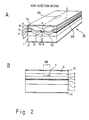
- the bistable DFB LD has a mesa stripe which includes an active layer 3, a waveguide layer 4 conjugate with the active layer 3 and provided with corrugation having a predetermined period, and a cladding layer 5 which holds the waveguide layer 4 between it and the active layer 3.
- the DFB LD includes an n-InP confining layer 7 provided on an intermediate portion of the mesa stripe, and a P-InP burying layer 8 and a cap layer 9.
- a voltage is applied across a positive electrode 10 and a negative electrode 11 to inject current into the active layer 3.
- the particular part of the active layer 3 located below the confining layer 7 defines a non-injection region where current injection does not occur, so that the light output shows a bistable characteristic.
- the procedure for manufacturing the DFB LD 20 will be described later in detail.
- the coupling resistor 23 had a resistance value of 50 2 and the coupling capacitor 24 a capacitance of 1 ⁇ F in order to suppress leakage of electricity between the bias circuit 21 and the drive circuit 22.
- An output signal of a 450 MHz pseudo-random pulse generator was used as an input signal for operating the light transmitter.
- the evaluation showed that the bistable DFB LD 20 generates optical signal pulses which follow the input signal, and that the optical pulses are each 7 mW high.
- the spectrum of the modulated light signal was found by evaluation to be similar to the spectrum shown in FIG. 4B and, in addition, optical signals modulated by random pulses also had a lasin g spectrum line width as narrow as about 600 MHz.
- Transmission tests were conducted by introducing optical signals provided by the optical transmitter of the present invention into single mode fibers having a core diameter of 10 ⁇ m through an optical lens arrangement and with a coupling loss of 2 dB.
- a receiver used for the tests was implemented with a Ge-APD having a light receiving diameter of 80 ⁇ m.
- the received power level of the receiver was -42 dBm for a bit error rate of 10 -10 S -1 .
- optical fibers which show an average transmission loss of 0.25 dB/km inclusive of splice losses of the optical fibers at the wavelength in the 1.55 ⁇ m band was used, the transmitter successfully transmitted signals over a distance of 160 km with a margin of 2 dBm.
- the bias current I b when the bias current I b was increased so as to modulate the bistable DFB LD 20 in such a manner as not to traverse the hysteresis region, that is, when the bias current I b was controlled to a value between I ON ,t h and I OFF,th and the pulse current was superposed on such a bias current I b for modulation, the spectrum line width measured about 3 GHz with the result that the transmissible range was limited to 100 km due to the influence of wavelength dispersion.
- the DFB LD 20 comprises a (001) n-InP substrate 1 on which are sequentially grown an n-InP buffer layer 2 (Sn-doped, carrier density of 5 x 10 17 cm- 3 , thickness of 3 ⁇ m), a non-doped InGaAsP active layer 3 (1.3 ⁇ m composition in terms of emission wavelength, thickness of 0.1 ⁇ m), and p-InGaAsP guide layer 4 (1.1 ⁇ m composition in terms of emission wavelength, Zn-doped, carrier density of 7 x 10 18 cm -3 , thickness of 0.2 ⁇ m).
- n-InP buffer layer 2 Sn-doped, carrier density of 5 x 10 17 cm- 3 , thickness of 3 ⁇ m
- a non-doped InGaAsP active layer 3 1.3 ⁇ m composition in terms of emission wavelength, thickness of 0.1 ⁇ m
- p-InGaAsP guide layer 4 1.1 ⁇ m composition in terms of emission wavelength, Zn-d
- the p-InGaAsP guide layer 4 is provided with a diffraction grating 200 having a period of 2000 A and a depth of 1000 A.
- a p-InP cladding layer 5 (Zn-doped, carrier density of 1 x 10 18 cm -3 , and thickness of 1 ⁇ m) is deposited on the surface of the wafer which has been provided with the diffraction grating 200.
- a p-InP blocking layer 6 Zn-doped, carrier density of 1 x 10 18 cm -3 , 0.5 ⁇ m thick in flat portion
- an n-InP confining layer.7 Te-doped, carrier density of 3 x 10 18 cm -3 , 0.5 ⁇ m thick in flat portion
- a p-InP burying layer 8 Zn-doped, carrier density of 1 x 10 18 cm -3 , 1.5 ⁇ m thick in flat portion
- a p-InGaAsP cap layer 9 1.2 ⁇ m thick composition in terms of emission wavelength, Z-doped, carrier density of 1 x 1 0 19 cm -3 , about 1 ⁇ m thick in a flat portion
- the n-InP confining layer 7 is laminated exclusively on that part of the mesa stripe 50 which lies in the non-injection region 100. To grown the confining layer 7 only in the limited region 100, the two channels 51 and 52 may each be narrowed in the specific region 100. In the non-injection region 100, the confining layer 7 serves to prevent a current from being injected into the InGaAsP active layer 3 which is located beneath the confining layer 7.
- bistable DFB LD While only basic structural elements are shown in the embodiment of Fig. 1, it will be noted that a temperature control unit for controlling the operation temperature of the bistable DFB LD to a predetermined value, a light isolator for reducing the influence of light returning to the DFB LD, and others may be incorporated, if desired. It should be born in mind that the bistable DFB LD structure and current values shown and described are merely typical examples and not restrictive in any way, that is, the present invention is applicable to any kind of DFB LDs.
- the present invention provides an optical transmitter which offers a remarkable improvement in transmissible distance over prior art transmitters.
- This advantage is derived from the fact that since the transmitter of the present invention is capable of generating signal pulses having a narrow lasing spectrum line width, it is free from the limitation due to wavelength dispersion of optical fibers when applied to an optical fiber communications system.
Landscapes
- Physics & Mathematics (AREA)
- Condensed Matter Physics & Semiconductors (AREA)
- General Physics & Mathematics (AREA)
- Electromagnetism (AREA)
- Optics & Photonics (AREA)
- Optical Communication System (AREA)
- Semiconductor Lasers (AREA)
Applications Claiming Priority (2)
| Application Number | Priority Date | Filing Date | Title |
|---|---|---|---|
| JP159823/84 | 1984-07-30 | ||
| JP15982384A JPS6139643A (ja) | 1984-07-30 | 1984-07-30 | 光送信装置 |
Publications (3)
| Publication Number | Publication Date |
|---|---|
| EP0171027A2 true EP0171027A2 (de) | 1986-02-12 |
| EP0171027A3 EP0171027A3 (en) | 1988-12-21 |
| EP0171027B1 EP0171027B1 (de) | 1991-12-04 |
Family
ID=15702027
Family Applications (1)
| Application Number | Title | Priority Date | Filing Date |
|---|---|---|---|
| EP85109595A Expired - Lifetime EP0171027B1 (de) | 1984-07-30 | 1985-07-30 | Optischer Sender |
Country Status (4)
| Country | Link |
|---|---|
| US (1) | US4947458A (de) |
| EP (1) | EP0171027B1 (de) |
| JP (1) | JPS6139643A (de) |
| DE (1) | DE3584801D1 (de) |
Cited By (1)
| Publication number | Priority date | Publication date | Assignee | Title |
|---|---|---|---|---|
| EP0193819A1 (de) * | 1985-03-04 | 1986-09-10 | Hitachi, Ltd. | Einrichtung zum Verstärken und Formen von optischen Impulsen |
Families Citing this family (2)
| Publication number | Priority date | Publication date | Assignee | Title |
|---|---|---|---|---|
| US20010048799A1 (en) * | 1998-05-21 | 2001-12-06 | F. David King | Optical communication system |
| US6944404B2 (en) * | 2000-12-11 | 2005-09-13 | Harris Corporation | Network transceiver for extending the bandwidth of optical fiber-based network infrastructure |
Family Cites Families (11)
| Publication number | Priority date | Publication date | Assignee | Title |
|---|---|---|---|---|
| US3680001A (en) * | 1971-05-13 | 1972-07-25 | Bell Telephone Labor Inc | Dynamic am control of the transverse modes of a self-pulsing semiconductor laser |
| JPS5967677A (ja) * | 1982-07-01 | 1984-04-17 | Semiconductor Res Found | 光集積回路 |
| JPS5992587A (ja) * | 1982-11-18 | 1984-05-28 | Nec Corp | 光増幅回路 |
| CA1206633A (en) * | 1982-11-29 | 1986-06-24 | Kunio Nagashima | Optical time-division switching system employing optical bistable devices |
| JPS59117285A (ja) * | 1982-12-24 | 1984-07-06 | Nec Corp | 光増幅回路 |
| JPS59182637A (ja) * | 1983-03-31 | 1984-10-17 | Matsushita Electric Ind Co Ltd | ビデオ信号光伝送装置 |
| US4558465A (en) * | 1983-09-19 | 1985-12-10 | Rca Corporation | Switched bias scheme for high speed laser transmitter |
| JPS6079788A (ja) * | 1983-10-06 | 1985-05-07 | Nec Corp | 光双安定素子 |
| JPS6079786A (ja) * | 1983-10-06 | 1985-05-07 | Nec Corp | 双安定レ−ザ |
| JPS60102789A (ja) * | 1983-11-09 | 1985-06-06 | Kokusai Denshin Denwa Co Ltd <Kdd> | 分布帰環形半導体レ−ザ |
| CA1210070A (en) * | 1984-10-26 | 1986-08-19 | Northern Telecom Limited | Laser transmitter |
-
1984
- 1984-07-30 JP JP15982384A patent/JPS6139643A/ja active Pending
-
1985
- 1985-07-30 US US06/760,560 patent/US4947458A/en not_active Expired - Fee Related
- 1985-07-30 EP EP85109595A patent/EP0171027B1/de not_active Expired - Lifetime
- 1985-07-30 DE DE8585109595T patent/DE3584801D1/de not_active Expired - Lifetime
Non-Patent Citations (4)
| Title |
|---|
| APPLIED PHYSICS LETTERS, vol. 40, no. 5, 1st March 1982, pages 369-371, American Institute of Physics, New York, US; K.Y. LAU et al.: "Interaction of a bistable injection laser with an external optical cavity" * |
| I.E.E. PROCEEDING SECTION A A I, vol. 129, no. 4, part I, August 1982, pages 141-148, Old Woking, Surrey, GB; H. KAWAGUCHI: "Optical bistable-switching operation in semiconductor lasers with inhomogeneous excitation" * |
| IEEE JOURNAL OF QUANTUM ELECTRONICS, vol. QE-18, no. 9, September 1982, pages 1351-1361, IEEE, New York, US; C. HARDER et al.: "Bistability and pulsations in semiconductor lasers with inhomogeneous current injection" * |
| IEEE JOURNAL OF QUANTUM ELECTRONICS, vol. QE-19, no. 6, June 1983, pages 1052-1056, IEEE, New York, US; S. AKIBA et al.: "Distributed feedback InGaAsP/InP lasers with window region emitting at 1.5 mum range" * |
Cited By (1)
| Publication number | Priority date | Publication date | Assignee | Title |
|---|---|---|---|---|
| EP0193819A1 (de) * | 1985-03-04 | 1986-09-10 | Hitachi, Ltd. | Einrichtung zum Verstärken und Formen von optischen Impulsen |
Also Published As
| Publication number | Publication date |
|---|---|
| EP0171027A3 (en) | 1988-12-21 |
| DE3584801D1 (de) | 1992-01-16 |
| US4947458A (en) | 1990-08-07 |
| JPS6139643A (ja) | 1986-02-25 |
| EP0171027B1 (de) | 1991-12-04 |
Similar Documents
| Publication | Publication Date | Title |
|---|---|---|
| US5590145A (en) | Light-emitting apparatus capable of selecting polarization direction, optical communication system, and polarization modulation control method | |
| US5764670A (en) | Semiconductor laser apparatus requiring no external modulator, method of driving semiconductor laser device, and optical communication system using the semiconductor laser apparatus | |
| Koyama et al. | 1.5-1.6 µm GaInAsP/InP dynamic-single-mode (DSM) lasers with distributed Bragg reflector | |
| Takeuchi et al. | Very high-speed light-source module up to 40 Gb/s containing an MQW electroabsorption modulator integrated with a DFB laser | |
| US9564733B2 (en) | Method of fabricating and operating an optical modulator | |
| JPH06216467A (ja) | 半導体光分散補償器 | |
| US5850408A (en) | Method of driving semiconductor laser with wide modulation band, optical communication method, semiconductor laser device, node, and optical communication system | |
| JPH06103778B2 (ja) | 半導体分布帰還形レーザを含む光学装置およびその駆動方法 | |
| US4947400A (en) | Laser-photodetector assemblage | |
| Suzuki et al. | lambda/4-shifted DFB laser/electroabsorption modulator integrated light source for multigigabit transmission | |
| EP0171027B1 (de) | Optischer Sender | |
| Iwashita et al. | Mode partition noise characteristics in high-speed modulated laser diodes | |
| EP0189252A2 (de) | Halbleiterlaseranordnung mit direkter Frequenz-Modulation | |
| JPH08248364A (ja) | 光強度変調素子及び光強度変調素子付き半導体レーザ | |
| Yasaka et al. | Finely tunable wavelength conversion of high bit-rate signals by using a superstructure-grating distributed Bragg reflector laser | |
| Tsang et al. | The heteroepitaxial ridge-overgrown distributed feedback laser | |
| JP2616206B2 (ja) | 集積化光源装置 | |
| Ishizaka et al. | Modulator integrated DFB lasers with more than 600-km transmission capability at 2.5 Gb/s | |
| US5317448A (en) | Method for driving a laser amplifier with minimized distortion | |
| JP2001290114A (ja) | 光送信モジュール | |
| Debrégeas-Sillard et al. | New WDM optimized integrated laser-electroabsorption modulator for 1000-km 2.5-Gb/s transmission over a wide range of operating conditions | |
| JP3450573B2 (ja) | 半導体レーザ装置、その駆動方法及びそれを用いた光通信システム | |
| JPS6281086A (ja) | 光送信装置 | |
| JP7147611B2 (ja) | 高出力直接変調型レーザ | |
| Sasaki et al. | Selective MOVPE growth and its application to semiconductor photonic integrated circuits |
Legal Events
| Date | Code | Title | Description |
|---|---|---|---|
| PUAI | Public reference made under article 153(3) epc to a published international application that has entered the european phase |
Free format text: ORIGINAL CODE: 0009012 |
|
| 17P | Request for examination filed |
Effective date: 19850730 |
|
| AK | Designated contracting states |
Designated state(s): DE FR GB |
|
| PUAL | Search report despatched |
Free format text: ORIGINAL CODE: 0009013 |
|
| AK | Designated contracting states |
Kind code of ref document: A3 Designated state(s): DE FR GB |
|
| 17Q | First examination report despatched |
Effective date: 19910308 |
|
| GRAA | (expected) grant |
Free format text: ORIGINAL CODE: 0009210 |
|
| AK | Designated contracting states |
Kind code of ref document: B1 Designated state(s): DE FR GB |
|
| REF | Corresponds to: |
Ref document number: 3584801 Country of ref document: DE Date of ref document: 19920116 |
|
| ET | Fr: translation filed | ||
| PLBE | No opposition filed within time limit |
Free format text: ORIGINAL CODE: 0009261 |
|
| STAA | Information on the status of an ep patent application or granted ep patent |
Free format text: STATUS: NO OPPOSITION FILED WITHIN TIME LIMIT |
|
| 26N | No opposition filed | ||
| PGFP | Annual fee paid to national office [announced via postgrant information from national office to epo] |
Ref country code: FR Payment date: 19960705 Year of fee payment: 12 |
|
| PGFP | Annual fee paid to national office [announced via postgrant information from national office to epo] |
Ref country code: GB Payment date: 19960729 Year of fee payment: 12 |
|
| PGFP | Annual fee paid to national office [announced via postgrant information from national office to epo] |
Ref country code: DE Payment date: 19960927 Year of fee payment: 12 |
|
| PG25 | Lapsed in a contracting state [announced via postgrant information from national office to epo] |
Ref country code: GB Free format text: LAPSE BECAUSE OF NON-PAYMENT OF DUE FEES Effective date: 19970730 |
|
| GBPC | Gb: european patent ceased through non-payment of renewal fee |
Effective date: 19970730 |
|
| PG25 | Lapsed in a contracting state [announced via postgrant information from national office to epo] |
Ref country code: FR Free format text: LAPSE BECAUSE OF NON-PAYMENT OF DUE FEES Effective date: 19980331 |
|
| PG25 | Lapsed in a contracting state [announced via postgrant information from national office to epo] |
Ref country code: DE Free format text: LAPSE BECAUSE OF NON-PAYMENT OF DUE FEES Effective date: 19980401 |
|
| REG | Reference to a national code |
Ref country code: FR Ref legal event code: ST |