EP0170021B1 - Data processing system with a plurality of processors accessing a common bus to interleaved storage - Google Patents
Data processing system with a plurality of processors accessing a common bus to interleaved storage Download PDFInfo
- Publication number
- EP0170021B1 EP0170021B1 EP85107437A EP85107437A EP0170021B1 EP 0170021 B1 EP0170021 B1 EP 0170021B1 EP 85107437 A EP85107437 A EP 85107437A EP 85107437 A EP85107437 A EP 85107437A EP 0170021 B1 EP0170021 B1 EP 0170021B1
- Authority
- EP
- European Patent Office
- Prior art keywords
- storage
- bus
- address
- processors
- processor
- Prior art date
- Legal status (The legal status is an assumption and is not a legal conclusion. Google has not performed a legal analysis and makes no representation as to the accuracy of the status listed.)
- Expired
Links
Images

Classifications
-
- G—PHYSICS
- G06—COMPUTING OR CALCULATING; COUNTING
- G06F—ELECTRIC DIGITAL DATA PROCESSING
- G06F13/00—Interconnection of, or transfer of information or other signals between, memories, input/output devices or central processing units
- G06F13/14—Handling requests for interconnection or transfer
- G06F13/16—Handling requests for interconnection or transfer for access to memory bus
- G06F13/1605—Handling requests for interconnection or transfer for access to memory bus based on arbitration
- G06F13/1647—Handling requests for interconnection or transfer for access to memory bus based on arbitration with interleaved bank access
-
- G—PHYSICS
- G06—COMPUTING OR CALCULATING; COUNTING
- G06F—ELECTRIC DIGITAL DATA PROCESSING
- G06F13/00—Interconnection of, or transfer of information or other signals between, memories, input/output devices or central processing units
- G06F13/38—Information transfer, e.g. on bus
- G06F13/42—Bus transfer protocol, e.g. handshake; Synchronisation
- G06F13/4204—Bus transfer protocol, e.g. handshake; Synchronisation on a parallel bus
- G06F13/4208—Bus transfer protocol, e.g. handshake; Synchronisation on a parallel bus being a system bus, e.g. VME bus, Futurebus, Multibus
- G06F13/4217—Bus transfer protocol, e.g. handshake; Synchronisation on a parallel bus being a system bus, e.g. VME bus, Futurebus, Multibus with synchronous protocol
Definitions
- the present invention relates to data processing systems having a common bus connecting a plurality of processing units, such as a central processing unit and peripheral equipment control processors, to interleaved storage units.
- processing units such as a central processing unit and peripheral equipment control processors
- the interleaved storage means complements the pipelined common bus. Because storage operations are generally slower than the processors addressing the memory, the pipelined common bus gave processors the capability of sending addresses and other commands to memory or storage at a rate greater than basic storage units could handle. This resulted in the development of interleaved storage units wherein the address sent to storage from processors over the common bus addressed a plurality of interleaved memory units in sequence. As a result of this interleaving, each storage unit experiences a delay between addresses to it based upon the number of intermediate sequential interleaved storage units. As a result, the storage system can handle the addresses at a rate equivalent to the rate in which processors can provide such addresses.
- the present invention provides a data processing system wherein efficiency in sequentially accessing interleaved storage units from a common bus is maximized even in systems having a high frequency of switching access to the bus between a plurality of processors.
- the present invention provides an improvement wherein at least one of the processors includes means for monitoring the common bus to determine the last storage unit addressed prior to switching, and means responsive to these monitoring means for addressing the next storage unit in sequence. This continues the sequence of addressing the interleaved storage units substantially without any interruption.
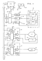
- Fig. 1 a generalized diagram of the apparatus which may be used in carrying out the present invention is shown.
- Common bus 10 is accessed by central processing unit 11, and by memory 12 which is connected to bus 10 via branch 13 as viii be hereinafter described in greater detail.
- processors 16 and 17 are connected with bus 10 through branches 18 and 19 respectively connected with controllers 14 and 15 in processors 16 and 17.
- Processors 16 and 17 are respectively connected with peripheral equipment such as display 20, keyboard 21 or I/O terminal 22, and act to control these I/O devices.
- Processors 16 and 17 are conventional as far as the control of the I/O equipment is concerned.
- Processors 16 and 17 may exchange data with CPU 11 via bus 10.
- the present invention is primarily concerned with the transmission of information between CPU 11 and interleaved memory 12, as well as between processors 16 and 17 and memory 12.
- CPU 11 may be any conventional processor using pipelining operations.
- the system is one having synchronized overlapped transactions on the common bus 10 under the control of clock 23 which produces on line 24 clock pulses (CLK) which are applied to CPU 11, storage controller 25, and processor controllers 14 and 15, respectively via lines 26, 27, 28 and 29.
- CLK clock pulses
- the pipelining is carried out in a conventional manner, e.g. in the manner described in U.S. patent 3,447,135. With such pipelining, transactions from the CPU or from peripheral devices via processors 16 and 17 to and from main memory 12 may be overlapped on common bus 10.
- common bus 10 need not be locked into a single transaction; when a transaction, from either the CPU 11 or processors 16 and 17 is initiated with respect to memory 12 over bus 10, the bus is not locked in until the transaction is completed, e.g., until read data is returned from memory.
- the present invention is primarily concerned with how memory 12, which consists of a pair of interleaved storage banks 1 and 2, is sequentially addressed as to maximize efficiency of addressing from CPU 11 and processors 16 and 17 to interleaved storage banks 1 and 2 via common bus 10.
- Any transaction involving information from either CPU 11 or processors 16 and 17 to memory 12 is connected from the respective processors to memory 12 via common bus 10 and branch 13, under the control of storage controller 25. If the particular processor is granted access to common bus 10 by the priority arrangement to be subsequently described then, if the data is an address, it proceeds through controller 25 to address buffer 32. If buffer 32 is not busy and can handle the address, an acknowledgement (ACK) is sent on line 33 from storage controller 25 and is respectively applied to CPU 11 and controllers 14 and 15 via lines 34, 35 and 36. Then, as will be hereinafter described in greater detail, the address from buffer 32 is applied either to storage buffer 37 of storage bank 1 or to storage buffer 38 of storage bank 2 in alternating sequence.
- ACK acknowledgement
- CPU 11 as well as processors 16 and 17 provide addresses to bus 10 during transfer intervals defined by clock 23 at a rate such that input of addresses to address buffer 32 is faster than the time required for completion of the transfer to either storage buffer 37 or storage buffer 38. Consequently, the need for two interleaved storage banks 1 and 2, i.e., while a first transfer to storage buffer 37 of storage bank 1 is being completed, a subsequent transfer from address register 32 to storage buffer 38 of storage bank 2 may be commenced and so on alternatively transferring addresses to storage buffers 37 and 38.
- the time required to complete an address transfer i.e., a transfer from a processor through address buffer 32 to either storage bank 1 or storage bank 2 represents only a portion of a storage read or write transaction. For example, if data is to be written into storage, it is transferred at some interval subsequent to the address interval from the source processor (11, 16 or 17) via bus 10, branch 13, controller 25 and data buffer 39. On the other hand, if data is to be read out of the addresss storage bank 1 or 2, then at some subsequent cycle it is read out via lines 40 and 41 and applied to output buffer 42 from which it is transferred to the respective requesting processor (11, 16 or 17) via line 43, controller 25, branch 13 and bus 10.
- the data to and from processors 16 and 17 relative to memory 12 is to be used by the I/O devices 20, 21 and 22.
- Data read from storage for these devices is respectively stored in input buffers 44 and 45, while data to be written into storage from these devices is respectively stored in output buffers 46 and 47 in processors 16 and 17.
- the key aspect of the present invention is how storage banks 1 and 2 are alternately addressed in sequence with addresses from the common bus 10 irrespective of the processor 11, 16 or 17 from which the address is transmitted on to bus 10.
- each of the processors has internal capability of transmitting a sequence of addresses onto bus 10 which alternately address bank 1 and then bank 2.
- the embodiment of the present invention relates to how this sequence is maintained when access to common bus 10 is switched from one of the processors 11, 16 or 17 to another.
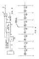
- Monitor latches 3 and 4 (Fig. 1) monitor common bus 10 in order to determine whether the last address transfer on the bus has been to storage bank 1 or storage bank 2. Further details are shown in Fig. 2.
- the monitor latch senses the common bus 10 through connector 49.
- a convenient arrangement is to have one bit in the address command sent on bus 10 representative of the storage bank. Thus, if the bit is up, the address has to be transferred to storage bank 1 and if the bit is down, the address is to be transferred to storage bank 2. Conveniently this can be the low order bit in the address.
- the monitor latch is a conventional latch which responds to the clock signal to latch the bit and thus save it until the clock signal in the next cycle.
- the saved bit is thus available and is provided to the odd/even control logic circuitry 50 which is a series of standard logic gates operating in accordance with the flow chart of Fig. 3 to control the operations described in Fig. 3.
- step 51 when a request for an address transfer to storage comes up in CPU 11, it makes a determination, decision step 51, that it has a request to address storage. Then, step 52, the CPU indulges in arbitration for the bus.
- the arbitration scheme may be any conventional scheme wherein the three processors, i.e., CPU 11, and processors 16 and 17 (Fig. 1) contend for access and control of common bus 10. These are many and varied in the prior art described hereinabove.
- the present system utilizes a rather simple straight forward daisy chain approach wherein a predetermined priority is established which in the present case is that processor 17 has priority over processor 16 which in turn has priority over CPU 11. In the case where there is no request for the bus (step 51, Fig.
- the arbitration step 52 will give the bus to CPU 11 until such time as CPU 11 loses control of the bus to a higher priority processor. Whether a higher priority processor, i.e., processor 16 or 17, has control of the bus is determined in decision step 53. So long as another processor does not take control of bus 10, CPU 11 will retain control and will send out a series of alternate addresses to storage banks 1 and 2 (Fig. 1). This is illustrated in Fig. 4 by the sequence of the four time periods t0 to t3.
- step t5 address A'1 in processor 17 will go to storage bank 1.
- This address is put out on the driver bus line 58 in the control logic 50 in Fig. 2 and applied to bus 10.
- Processor 17 is now ready to put out its next address A'2 alternatively to bank 2 (Fig. 4). In order to do so, it must again arbitrate for the bus, step 59 (Fig. 3). It does so by providing a signal from the odd/even control logic 50 on line 60 to OR-gate 61 and then the bus request line 62. If in decision step 63 a determination is made that processor 17 no longer has the bus, the operation is returned to step 59 wherein the processor 17 once again contends for the bus. After the determination is made, step 63, that the processor still has the bus, the operation proceeds to step 65, wherein an address with an even bit indicating a transfer to storage bank 2 is selected and transferred as previously described.
- step 66 a determination is made as to whether the previous address was the last address which processor 17 had to transfer to memory. If it is, then the system is returned to step 51. If there are still additional addresses to be transferred from processor 17, then, there is another arbitration for the bus, step 67. If by decision step 68, processor 17 still has access to the bus, the system is returned to step 57 and steps 57-66 are repetitively carried out to send alternating pairs of addresses sequentially to storage banks 1 and 2 until the point when processor 17 has no further addresses to send.
- Step 57 the last address from the CPU to the interleaved storage unit 12 had been to bank 1 instead of bank 2, then the "No" branch would have been taken and steps 77-88 would be carried out. Steps 77-88 are substantially equivalent to the steps 57-68, respectively, except that the initial address put out is an address with an even bit indicating a transfer to storage bank 2.
Landscapes
- Engineering & Computer Science (AREA)
- Theoretical Computer Science (AREA)
- Physics & Mathematics (AREA)
- General Engineering & Computer Science (AREA)
- General Physics & Mathematics (AREA)
- Multi Processors (AREA)
- Memory System (AREA)
- Bus Control (AREA)
Applications Claiming Priority (2)
| Application Number | Priority Date | Filing Date | Title |
|---|---|---|---|
| US06/636,188 US4669056A (en) | 1984-07-31 | 1984-07-31 | Data processing system with a plurality of processors accessing a common bus to interleaved storage |
| US636188 | 1984-07-31 |
Publications (3)
| Publication Number | Publication Date |
|---|---|
| EP0170021A2 EP0170021A2 (en) | 1986-02-05 |
| EP0170021A3 EP0170021A3 (en) | 1988-05-25 |
| EP0170021B1 true EP0170021B1 (en) | 1991-10-16 |
Family
ID=24550825
Family Applications (1)
| Application Number | Title | Priority Date | Filing Date |
|---|---|---|---|
| EP85107437A Expired EP0170021B1 (en) | 1984-07-31 | 1985-06-19 | Data processing system with a plurality of processors accessing a common bus to interleaved storage |
Country Status (5)
| Country | Link |
|---|---|
| US (1) | US4669056A (OSRAM) |
| EP (1) | EP0170021B1 (OSRAM) |
| JP (1) | JPS6142049A (OSRAM) |
| CA (1) | CA1225749A (OSRAM) |
| DE (1) | DE3584402D1 (OSRAM) |
Families Citing this family (26)
| Publication number | Priority date | Publication date | Assignee | Title |
|---|---|---|---|---|
| US4797815A (en) * | 1985-11-22 | 1989-01-10 | Paradyne Corporation | Interleaved synchronous bus access protocol for a shared memory multi-processor system |
| DE3785958D1 (de) * | 1986-04-02 | 1993-07-01 | Siemens Ag | Verfahren zum ansteuern eines gemeinsamen speichers eines aus einzelnen mikroprozessorsystemen bestehenden mehrprozessorsystems. |
| JPS6356754A (ja) * | 1986-08-28 | 1988-03-11 | Toshiba Corp | 入出力チヤネル |
| EP0261751A3 (en) * | 1986-09-25 | 1990-07-18 | Tektronix, Inc. | Concurrent memory access system |
| US5123100A (en) * | 1989-01-13 | 1992-06-16 | Nec Corporation | Timing control method in a common bus system having delay and phase correcting circuits for transferring data in synchronization and time division slot among a plurality of transferring units |
| US5283870A (en) * | 1991-10-04 | 1994-02-01 | Bull Hn Information Systems Inc. | Method and apparatus for avoiding processor deadly embrace in a multiprocessor system |
| US5412788A (en) * | 1992-04-16 | 1995-05-02 | Digital Equipment Corporation | Memory bank management and arbitration in multiprocessor computer system |
| US5404464A (en) * | 1993-02-11 | 1995-04-04 | Ast Research, Inc. | Bus control system and method that selectively generate an early address strobe |
| US5537555A (en) * | 1993-03-22 | 1996-07-16 | Compaq Computer Corporation | Fully pipelined and highly concurrent memory controller |
| US5630056A (en) * | 1994-09-20 | 1997-05-13 | Stratus Computer, Inc. | Digital data processing methods and apparatus for fault detection and fault tolerance |
| US5590299A (en) * | 1994-10-28 | 1996-12-31 | Ast Research, Inc. | Multiprocessor system bus protocol for optimized accessing of interleaved storage modules |
| US6446141B1 (en) | 1999-03-25 | 2002-09-03 | Dell Products, L.P. | Storage server system including ranking of data source |
| US6735715B1 (en) | 2000-04-13 | 2004-05-11 | Stratus Technologies Bermuda Ltd. | System and method for operating a SCSI bus with redundant SCSI adaptors |
| US6691257B1 (en) | 2000-04-13 | 2004-02-10 | Stratus Technologies Bermuda Ltd. | Fault-tolerant maintenance bus protocol and method for using the same |
| US6633996B1 (en) | 2000-04-13 | 2003-10-14 | Stratus Technologies Bermuda Ltd. | Fault-tolerant maintenance bus architecture |
| US6820213B1 (en) | 2000-04-13 | 2004-11-16 | Stratus Technologies Bermuda, Ltd. | Fault-tolerant computer system with voter delay buffer |
| US6708283B1 (en) | 2000-04-13 | 2004-03-16 | Stratus Technologies, Bermuda Ltd. | System and method for operating a system with redundant peripheral bus controllers |
| US6687851B1 (en) | 2000-04-13 | 2004-02-03 | Stratus Technologies Bermuda Ltd. | Method and system for upgrading fault-tolerant systems |
| US6948010B2 (en) | 2000-12-20 | 2005-09-20 | Stratus Technologies Bermuda Ltd. | Method and apparatus for efficiently moving portions of a memory block |
| US6766479B2 (en) | 2001-02-28 | 2004-07-20 | Stratus Technologies Bermuda, Ltd. | Apparatus and methods for identifying bus protocol violations |
| US7065672B2 (en) * | 2001-03-28 | 2006-06-20 | Stratus Technologies Bermuda Ltd. | Apparatus and methods for fault-tolerant computing using a switching fabric |
| US6996750B2 (en) * | 2001-05-31 | 2006-02-07 | Stratus Technologies Bermuda Ltd. | Methods and apparatus for computer bus error termination |
| JP2004355271A (ja) * | 2003-05-28 | 2004-12-16 | Toshiba Corp | データ転送システム |
| JP4765260B2 (ja) * | 2004-03-31 | 2011-09-07 | 日本電気株式会社 | データ処理装置およびその処理方法ならびにプログラムおよび携帯電話装置 |
| JP4416694B2 (ja) * | 2005-05-12 | 2010-02-17 | 株式会社ソニー・コンピュータエンタテインメント | データ転送調停装置およびデータ転送調停方法 |
| US8010764B2 (en) * | 2005-07-07 | 2011-08-30 | International Business Machines Corporation | Method and system for decreasing power consumption in memory arrays having usage-driven power management |
Family Cites Families (18)
| Publication number | Priority date | Publication date | Assignee | Title |
|---|---|---|---|---|
| US3447135A (en) * | 1966-08-18 | 1969-05-27 | Ibm | Peripheral data exchange |
| US4048623A (en) * | 1974-09-25 | 1977-09-13 | Data General Corporation | Data processing system |
| US3997896A (en) * | 1975-06-30 | 1976-12-14 | Honeywell Information Systems, Inc. | Data processing system providing split bus cycle operation |
| JPS5911980B2 (ja) * | 1975-12-23 | 1984-03-19 | 日本電気株式会社 | ランダムアクセスメモリソウチ |
| JPS52125243A (en) * | 1976-04-14 | 1977-10-20 | Fujitsu Ltd | Memory access control system |
| US4130885A (en) * | 1976-08-19 | 1978-12-19 | Massachusetts Institute Of Technology | Packet memory system for processing many independent memory transactions concurrently |
| US4128882A (en) * | 1976-08-19 | 1978-12-05 | Massachusetts Institute Of Technology | Packet memory system with hierarchical structure |
| US4228496A (en) * | 1976-09-07 | 1980-10-14 | Tandem Computers Incorporated | Multiprocessor system |
| JPS5417643A (en) * | 1977-07-08 | 1979-02-09 | Mitsubishi Electric Corp | Central processor |
| US4232366A (en) * | 1978-10-25 | 1980-11-04 | Digital Equipment Corporation | Bus for a data processing system with overlapped sequences |
| US4280176A (en) * | 1978-12-26 | 1981-07-21 | International Business Machines Corporation | Memory configuration, address interleaving, relocation and access control system |
| ES489424A0 (es) * | 1979-03-12 | 1981-02-16 | Digital Equipment Corp | Perfeccionamientos introducidos en un aparato de tratamien- to de datos de informacion. |
| JPS57121746A (en) * | 1981-01-22 | 1982-07-29 | Nec Corp | Information processing device |
| JPS57142441A (en) * | 1981-02-26 | 1982-09-03 | Isamu Iwase | Solar-heat collecting apparatus |
| JPS592135A (ja) * | 1982-06-28 | 1984-01-07 | Nec Corp | デ−タのブロツク転送方式 |
| US4564899A (en) * | 1982-09-28 | 1986-01-14 | Elxsi | I/O Channel bus |
| AU559558B2 (en) * | 1982-06-30 | 1987-03-12 | Elxsi | I/o channel bus |
| US4494192A (en) * | 1982-07-21 | 1985-01-15 | Sperry Corporation | High speed bus architecture |
-
1984
- 1984-07-31 US US06/636,188 patent/US4669056A/en not_active Expired - Lifetime
-
1985
- 1985-05-15 CA CA000481595A patent/CA1225749A/en not_active Expired
- 1985-05-17 JP JP10412485A patent/JPS6142049A/ja active Granted
- 1985-06-19 DE DE8585107437T patent/DE3584402D1/de not_active Expired - Lifetime
- 1985-06-19 EP EP85107437A patent/EP0170021B1/en not_active Expired
Also Published As
| Publication number | Publication date |
|---|---|
| EP0170021A2 (en) | 1986-02-05 |
| JPS6142049A (ja) | 1986-02-28 |
| US4669056A (en) | 1987-05-26 |
| DE3584402D1 (de) | 1991-11-21 |
| EP0170021A3 (en) | 1988-05-25 |
| JPH0449144B2 (OSRAM) | 1992-08-10 |
| CA1225749A (en) | 1987-08-18 |
Similar Documents
| Publication | Publication Date | Title |
|---|---|---|
| EP0170021B1 (en) | Data processing system with a plurality of processors accessing a common bus to interleaved storage | |
| EP0009678B1 (en) | Computer input/output apparatus | |
| US4050097A (en) | Synchronization technique for data transfers over an asynchronous common bus network coupling data processing apparatus | |
| US3993981A (en) | Apparatus for processing data transfer requests in a data processing system | |
| US4961140A (en) | Apparatus and method for extending a parallel synchronous data and message bus | |
| CA1184311A (en) | Peripheral interface adapter circuit for use in i/o controller card having multiple modes of operation | |
| US3995258A (en) | Data processing system having a data integrity technique | |
| US4519034A (en) | I/O Bus clock | |
| EP0476990B1 (en) | Dynamic bus arbitration | |
| US3940743A (en) | Interconnecting unit for independently operable data processing systems | |
| JP3645281B2 (ja) | 共用メモリを有するマルチプロセッサ・システム | |
| US4253147A (en) | Memory unit with pipelined cycle of operations | |
| US4185323A (en) | Dynamic memory system which includes apparatus for performing refresh operations in parallel with normal memory operations | |
| EP0451516B1 (en) | Improved SCSI device in a small computer system | |
| US4115854A (en) | Channel bus controller | |
| EP0321628B1 (en) | Shared memory interface for a data processing system | |
| JPS60186956A (ja) | デジタルデ−タ処理システムの入/出力部のためのバツフア装置 | |
| EP0288650B1 (en) | Protocol and apparatus for a control link between a control unit and several devices | |
| JPS58222363A (ja) | 共用メモリの割振装置 | |
| US5761728A (en) | Asynchronous access system controlling processing modules making requests to a shared system memory | |
| EP0309330B1 (en) | Access priority control system for main storage for computer | |
| CA2045063C (en) | Dual interleaved output queue | |
| EP0180299B1 (en) | Error detection system for a data processing apparatus | |
| US5671370A (en) | Alternating data valid control signals for high performance data transfer | |
| US4722052A (en) | Multiple unit adapter |
Legal Events
| Date | Code | Title | Description |
|---|---|---|---|
| PUAI | Public reference made under article 153(3) epc to a published international application that has entered the european phase |
Free format text: ORIGINAL CODE: 0009012 |
|
| AK | Designated contracting states |
Designated state(s): DE FR GB IT |
|
| 17P | Request for examination filed |
Effective date: 19860523 |
|
| PUAL | Search report despatched |
Free format text: ORIGINAL CODE: 0009013 |
|
| RHK1 | Main classification (correction) |
Ipc: G06F 13/18 |
|
| AK | Designated contracting states |
Kind code of ref document: A3 Designated state(s): DE FR GB IT |
|
| 17Q | First examination report despatched |
Effective date: 19890926 |
|
| GRAA | (expected) grant |
Free format text: ORIGINAL CODE: 0009210 |
|
| AK | Designated contracting states |
Kind code of ref document: B1 Designated state(s): DE FR GB IT |
|
| REF | Corresponds to: |
Ref document number: 3584402 Country of ref document: DE Date of ref document: 19911121 |
|
| ITF | It: translation for a ep patent filed | ||
| ET | Fr: translation filed | ||
| PLBE | No opposition filed within time limit |
Free format text: ORIGINAL CODE: 0009261 |
|
| STAA | Information on the status of an ep patent application or granted ep patent |
Free format text: STATUS: NO OPPOSITION FILED WITHIN TIME LIMIT |
|
| 26N | No opposition filed | ||
| PGFP | Annual fee paid to national office [announced via postgrant information from national office to epo] |
Ref country code: FR Payment date: 19960607 Year of fee payment: 12 |
|
| PGFP | Annual fee paid to national office [announced via postgrant information from national office to epo] |
Ref country code: DE Payment date: 19960628 Year of fee payment: 12 |
|
| PG25 | Lapsed in a contracting state [announced via postgrant information from national office to epo] |
Ref country code: FR Free format text: LAPSE BECAUSE OF NON-PAYMENT OF DUE FEES Effective date: 19980227 |
|
| PG25 | Lapsed in a contracting state [announced via postgrant information from national office to epo] |
Ref country code: DE Free format text: LAPSE BECAUSE OF NON-PAYMENT OF DUE FEES Effective date: 19980303 |
|
| REG | Reference to a national code |
Ref country code: FR Ref legal event code: ST |
|
| REG | Reference to a national code |
Ref country code: FR Ref legal event code: ST |
|
| PGFP | Annual fee paid to national office [announced via postgrant information from national office to epo] |
Ref country code: GB Payment date: 20010604 Year of fee payment: 17 |
|
| REG | Reference to a national code |
Ref country code: GB Ref legal event code: IF02 |
|
| PG25 | Lapsed in a contracting state [announced via postgrant information from national office to epo] |
Ref country code: GB Free format text: LAPSE BECAUSE OF NON-PAYMENT OF DUE FEES Effective date: 20020619 |
|
| GBPC | Gb: european patent ceased through non-payment of renewal fee |
Effective date: 20020619 |