EP0168633A2 - Schaltungsanordnung zur Matrixauswahl für Direktzugriffsspeicher - Google Patents
Schaltungsanordnung zur Matrixauswahl für Direktzugriffsspeicher Download PDFInfo
- Publication number
- EP0168633A2 EP0168633A2 EP85107230A EP85107230A EP0168633A2 EP 0168633 A2 EP0168633 A2 EP 0168633A2 EP 85107230 A EP85107230 A EP 85107230A EP 85107230 A EP85107230 A EP 85107230A EP 0168633 A2 EP0168633 A2 EP 0168633A2
- Authority
- EP
- European Patent Office
- Prior art keywords
- bit
- transistor
- circuit
- word
- collector
- Prior art date
- Legal status (The legal status is an assumption and is not a legal conclusion. Google has not performed a legal analysis and makes no representation as to the accuracy of the status listed.)
- Granted
Links
Images


Classifications
-
- G—PHYSICS
- G11—INFORMATION STORAGE
- G11C—STATIC STORES
- G11C11/00—Digital stores characterised by the use of particular electric or magnetic storage elements; Storage elements therefor
- G11C11/21—Digital stores characterised by the use of particular electric or magnetic storage elements; Storage elements therefor using electric elements
- G11C11/34—Digital stores characterised by the use of particular electric or magnetic storage elements; Storage elements therefor using electric elements using semiconductor devices
- G11C11/40—Digital stores characterised by the use of particular electric or magnetic storage elements; Storage elements therefor using electric elements using semiconductor devices using transistors
- G11C11/41—Digital stores characterised by the use of particular electric or magnetic storage elements; Storage elements therefor using electric elements using semiconductor devices using transistors forming static cells with positive feedback, i.e. cells not needing refreshing or charge regeneration, e.g. bistable multivibrator or Schmitt trigger
- G11C11/413—Auxiliary circuits, e.g. for addressing, decoding, driving, writing, sensing, timing or power reduction
- G11C11/414—Auxiliary circuits, e.g. for addressing, decoding, driving, writing, sensing, timing or power reduction for memory cells of the bipolar type
- G11C11/416—Read-write [R-W] circuits
-
- G—PHYSICS
- G11—INFORMATION STORAGE
- G11C—STATIC STORES
- G11C11/00—Digital stores characterised by the use of particular electric or magnetic storage elements; Storage elements therefor
- G11C11/21—Digital stores characterised by the use of particular electric or magnetic storage elements; Storage elements therefor using electric elements
- G11C11/34—Digital stores characterised by the use of particular electric or magnetic storage elements; Storage elements therefor using electric elements using semiconductor devices
- G11C11/40—Digital stores characterised by the use of particular electric or magnetic storage elements; Storage elements therefor using electric elements using semiconductor devices using transistors
- G11C11/41—Digital stores characterised by the use of particular electric or magnetic storage elements; Storage elements therefor using electric elements using semiconductor devices using transistors forming static cells with positive feedback, i.e. cells not needing refreshing or charge regeneration, e.g. bistable multivibrator or Schmitt trigger
- G11C11/413—Auxiliary circuits, e.g. for addressing, decoding, driving, writing, sensing, timing or power reduction
- G11C11/414—Auxiliary circuits, e.g. for addressing, decoding, driving, writing, sensing, timing or power reduction for memory cells of the bipolar type
- G11C11/415—Address circuits
Definitions
- the invention is directed to an improved random access memory (RAM). More particularly the invention is directed to improved selection circuitry for an array using CTS (Complementary Transistor Switch) memory cells.
- CTS Complementary Transistor Switch
- Random access memories employing CTS type memory cells are known to the art. See for the example, the Gersbach patent 3,863,229, the Dorler et al IBM TDB publication, and the Dorler et al IBM Journal of Research and Development Article, each fully identified hereinabove.
- bit decode transistor has to drive a number of bit columns across the chip. Due to long metal line and large fan out current, voltage drop along the bit decode line is high. The cells at the end of the bit decode line may have insufficient voltage across their "1" bit rail resistors to provide adequate gate currents into the cells. This may lead to potential data retention problems on the selected cells.
- both selection and deselection of the bit rails are slow due to the fact that the bit decode transistor has large fan-out loadings. Discharge speed of the bit rails is limited by the bit rail resistors.
- the bit selection scheme in accordance with the invention obviates the above recited short comings of known RAMs and in particular RAMs using CTS cells.
- the invention as claimed solves the problems of the slow speed of the word and bit line selection, the instability of the voltage along the word and bit lines and therefrom outcoming data retention problems of fully selected cells, and the long address set up time in "write" operation occurring in known RAMs, preferably in RAMs employing complementary transistor switch (CTS) cells.
- CTS complementary transistor switch
- the invention provides for an improved selection circuitry, whose word line selection part has a "voltage mode word selection scheme" for a RAM, in particular one using CTS (Complementary Transistor Switch) cells.
- the bit select circuitry includes interconnected first and second level matrix decoders, each memory column has a pair of bit lines, each pair of bit lines has connected thereto bit select circuit means, each of said bit select circuit means being connected to an output of said second level decoder, a bit up level clamp circuit connected to each of said bit select circuit means of each pair of bit lines, each of said bit select circuit means including first circuit means for increasing the speed of selection of the selected pair of bit lines, said bit up level clamp circuit cooperating with said bit select circuit means of said selected pair of bit lines for positively limiting the upper potential level of said selected pair of bit lines, and each of said bit select circuit means including second circuit means for increasing the speed of deselection of the selected pair of bit lines.
- the invention also includes voltage mode word selection means in a RAM preferably employing CTS type memory cells.
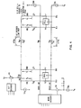
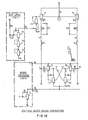
- Figure 2 shows a 1k x 4 RAM in accordance with the invention.
- This RAM has an array density of 4096 cells arranged in 64 words (rows) by 64 bit (columns). The 64 bit columns are further divided into 4 data groups, so that it will write 4 bits (therefore 4 data inputs) and read 4 bits (4 data outputs) at a time.
- the RAM has 6-bit word addresses (to select 1 out of 64 rows) and 4-bit bit addresses (to select 4 out of 64 bits). Read and write operations are controlled by the RW input.
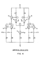
- the first level decode includes two groups of 4 address lines (BAO - BA3 and BA4 - BA7) formed from output emitter dotting of the four bit address receivers.
- the bit address receivers are current switch emitter follower circuits as shown in Figure 4. They convert the address inputs to true and complement signals. By means of emitter follower output dotting of the address receiver pairs, a partial decode of 1 out of 4 is formed from each group, hence, giving a total of two selected (low level) lines.
- the second level decode function is performed by the 16 bit decoders ( Figure 5), which have current switch inputs and high speed push-pull outputs.
- Input 1 of the bit decoder is connected to one of the 4 lines in BAO - BA3 address group, and input 2 is connected to one in the BA4 - BA7 group.
- Of the 16 BD output lines only one is decoded to a selected up level. Each BD line fans out to drive four bit columns (one from each data group), so that four cells are selected at a time for READ or WRITE operation.
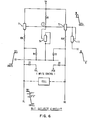
- Each bit column has a bit select circuit ( Figures 3 and 6) to perform bit line select and deselect functions.
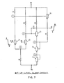
- the selected bit lines up level is set by a bit up level clamp circuit (Bit UPCL, Figure 7), so that the cells' read and write operating points can be readily adjusted by changing the up clamp (UC) level.
- the bit select circuit's modes of operation are described below.
- the BD line In an unselected state, the BD line is held low by its corresponding bit decoder to a voltage close to V N .
- Node 1 of the bit select circuit is clamped down by the base-collector diode T4.
- Bit lines BL and BR are also pulled negative to unselected levels by Schottk y diodes Dl and D2.
- resistor Rl provides a small DC current that conducts through T4 into the BD line. Since T4 conducts in saturation mode, it develops large diffusion capacitance (due to storage charge) across its B-C junction. The storage charge will be used to boot strap node 1 up rapidly when the BD line is selected high.
- both PDL and PDR lines are high (at around V P ), Schottky diodes D3 and D4 are OFF and will be out of the way.
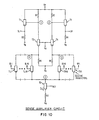
- Node 1's level is clamped by the transistor diode T3 to a voltage set by the UC line ( Figure 12).
- This READ reference level is generated by the bit up level clamp circuit in such a way that it will track with the selected cells' voltages to ensure proper READ currents (load current I L and gate current I G ).
- the read currents are supplied by T1 and T2 through resistors RBL and RBR into the cell.
- Typical READ currents are set at I L % 1.0 mA and IG ⁇ 0.2 mA. This results in a voltage differential of about 500-600 mV across the bit lines for READ sensing by the sense amplifier.
- the selected cell's read currents are sourced directly from Vp power supply and are distributed evenly across the array independent of BD line's voltage level.
- bit lines selection is similar to that of the READ mode as described above. The only difference here is that one of the WRITE control lines (either PDL or PDR, depending on the data to be written) is driven negative to a voltage close to V N by the write control circuit prior to bit line selection ( Figure 13).
- the lowered PDL or PDR line will clamp down BL or BR through Schottky diode D3 or D4 respectively, so that when the bit column is selected, only one side of the bit lines will go high to drive write current I w into the cell. The other side will stay at negative down level in order to shut off the bit line current that normally flows into the cell.
- This mode of write operation is denoted "Differential Mode Write" hereinafter.
- node l's up level is also clamped by diode T3 to a voltage set by the UC line.
- the write reference voltage is typically 600-800 mV above the READ reference voltage, so that sufficient write current is always guaranteed to ensure fast write performance.
- the write current is also sourced directly from V through Tl and T2. The write performance is therefore not affected by the BD line's level variations.
- bit column When a bit column is not selected, its corresponding bit decoder output falls to a low level. Node 1 of the bit select circuit is pulled negative by diode T4 to turn OFF Tl and T2. The bit lines, at the same time, are also pulled down actively by Schottky diodes Dl and D2 and will discharge into the BD line. After the bit lines are fully discharged to unselected down level, Dl and D2 will stop conducting. The bit column is said to be in an unselected state.
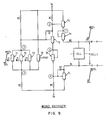
- the disclosed bit select scheme has particular utility in arrays using CTS (Complementary Transistor Switch, Figure 1A) cells. With this scheme, at least the following two advantages have been achieved over the known designs.
- the improved bit selection circuit means in accordance with the invention includes the following elements:
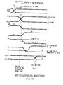
- the first level decode includes three groups of 4 address lines (WAO - WA3, WA4 - WA7, and WAS - WAll) formed from output emitter dotting of the 6 word address receivers.
- the word address receivers are current switch emitter follower circuits ( Figure 4). They convert the address inputs to true and complement signals. By means of emitter follower output dotting of the address receiver pairs, a partial decode of 1 out of 4 is obtained from each group, hence giving a total of three selected (low level) lines.
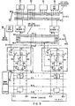
- the second level decode function is performed by the 64 word decoders ( Figure 9).
- Each word decoder has three current switch inputs (IN1 - IN3) and two high speed high power push-pull outputs (WL and DL).
- IN1 of the word decoders is connected to one of the four lines in WAO - WA3 address group.
- IN2 is connected to one in the second group (WA4 - WA7), and
- IN3 is connected to one in the third group (WA8 - WAll). All these three inputs have to be low in order to select a row line.
- the two outputs of the word decoder are connected to the word line (WL) and drain line (DL) of the memory cells as shown.
- An unselected word decoder will have at least one of its three inputs high.
- Decoding transistors T1, T2 or T3 are turned ON to pull down node 1.
- Transistors T5 and T6 form a dual phase level shifter, so that node 4 is also pulled negative to a voltage close to V and node 3 is pulled positive to Vp. With node 4 being down, the open collector transistor TL is shut off, allowing the word line WL and drain line DL to move up to their unselected (high) levels. In this state, the cells' stand-by current, as well as word and drain line voltages are defined by the current sources I SBH and I SBL .
- transistors T5 and T6 are never shut OFF but kept in slight conduction.
- the active pull up devices (T 7 and T H ) are OFF when the word line reaches its full unselected DC level (about one and half V BE below V P ).
- Transistors T1, T2 and T3 are OFF.
- Node 1 goes high to turn ON T5 and T6 hard.
- Node 3 is pulled down by T5's collector to keep T 7 - T H OFF, so that WL and DL are allowed to move down to their selected levels.
- node 4 is driven high to turn ON TL. It is this high power open collector pull down action on the drain line that enables the cells to be selected fast. While the drain line is being driven low, the word line follows it at the same rate with a voltage offset defined by the cells.
- T 7 - T H are OFF and TL is maintained ON to sink the large READ/WRITE currents conducting from the selected cells.
- the word and drain line voltages are defined by following two equations:
- a deselecting word decoder will have at least one of its inputs go positive.
- Decoding transistors Tl, T2 or T3 are turned ON again, driving node 1 down to shut OFF the open collector transistor T L .
- node 4 is pulled positive to Vp, driving the emitter follower devices T 7 - T H transiently ON to pull up word line WL until it reaches its unselected DC level.
- drain line DL follows it up at the same rate with a voltage offset defined by the cells.
- T 7 - T H and T L are all OFF. The row line is now said to be in an unselected state.
- a cell is selected for the READ operation when its row lines (WL, DL) and bit lines (BL, BR) are both selected ( Figure 12).
- the row lines are selected by the voltage mode word selection scheme as previously described.
- the bit lines are selected by the bit selection scheme explained earlier ( Figure 3).
- I L and I G are fed into its bit rail Schottky SL and SR, which then couple the cell's internal voltage ("0" and "1") on to the bit lines for READ sensing.
- I L and I G currents have to be controlled within a chosen operating range. This is accomplished by a READ reference level applied to the bit rail driving transistors (T 1 and T 2 of Figure 12) from the UC line.
- the READ reference is generated by a bit up level clamp circuit (Bit UPCL, Figure 7) which tracks fully with the selected cells, so that sufficient voltage potentials (V"0" and V"l") are always ensured across bit rail resistors RBL and RBR to define I L and I G currents.
- Bit up level clamp circuit Bit UPCL, Figure 7
- the magnitude of write current I W is also controlled by a WRITE reference level applied to the bit rail driving transistors T1 and T2 through the UC line. This write current can readily be adjusted by changing the bit up level clamp WRITE reference level.
- the key advantage of this write scheme is that since the drain line is selected to a fixed voltage offset from V N , when write current is injected into the cell, the level of this line will not move up but remain stable.
- the chasing effect with the deselecting cells as exists in "current mode" word selection scheme used by prior art designs is hence eliminated.
- the write pulse can now come in sooner (as soon as the selecting and deselecting drain lines cross over) without waiting for the deselecting cells to get out of the way. This minimizes address set up time required prior to write. Due to faster word selection and shorter address set up time, write performance is therefore greatly improved.
- the selected drain line is solidly held to a voltage level, and the deselected one is actively pulled up quickly to its unselected level, no "write through” (i.e., writing into the deselecting as well as the stand-by cells) problems exist.
- bit up level clamp circuit to define a selected cells' operating levels. This is particularly important for the READ operation.
- a read reference voltage is generated by the bit up level clamp to track with the selected cells in temperature, power supply (V N ) and device ( V BE and V FSBD ) variations, so that proper read currents (I G and I L ) are always guaranteed under all conditions to ensure cell stability.
- the bit up level clamp circuit ( Figure 7) represented in Figures 3 and 3A by the block labelled "BIT UPCL" will now be explained with particular reference to Figures 8, 12 and 13.
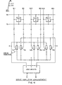
- sensing circuitry The operation of circuitry represented in Figure 3 by the block labelled “sensing circuitry" will now be explained with particular reference to Figures 10 and 11.
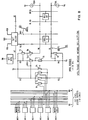
- FIG 3A illustrates the sensing scheme employed for the RAM shown in Figure 2.
- the 64 bit columns of this RAM is divided into four data groups of 16 bits.
- Each data group contains a sense amplifier ( Figure 10) for READ sensing.
- the state of the sense amplifier is determined by the selected cell within its data group.
- Data read by the sense amplifier is output off chip through an off chip driver (OCD) circuit.
- OCD off chip driver
- FIG 11 illustrates the sense amplifier arrangement for a data group.
- each bit column has a pair of sensing transistors (TL and TR) attached to its bit lines for voltage sensing.
- TL and TR sensing transistors
- Figure 10 illustrates a high speed sense amplifier circuit designed for the above sensing scheme.
- the circuit uses current steering technique to enable very fast switching performance. Its sensing speed is independent of the number of bit columns in the data group.
- the thirty-two sensing transistors T11 to TL16 and TR1 to TR16 form a big current switch input for the sense amplifier.
- the bases of these transistors are connected to the sixteen bit columns in the data group.
- Transistors Tl and T2 are emitter followers providing dual-phase outputs to drive the off chip driver.
- Transistors T3 and T4 are set to be ON all the time to define a fixed voltage at nodes A and B, so that switching of these two devices is done in current mode.
- bit-left or bit-right of a selected bit column is up at a high voltage level.
- the higher voltage bit line turns on its corresponding sensing transistor.
- the sense current IS from the current source T5 is then steered by the ON sensing transistor through either T3 or T4, pulling node 1 or 2 down accordingly.
Landscapes
- Engineering & Computer Science (AREA)
- Microelectronics & Electronic Packaging (AREA)
- Computer Hardware Design (AREA)
- Static Random-Access Memory (AREA)
Applications Claiming Priority (2)
| Application Number | Priority Date | Filing Date | Title |
|---|---|---|---|
| US624486 | 1984-06-25 | ||
| US06/624,486 US4578779A (en) | 1984-06-25 | 1984-06-25 | Voltage mode operation scheme for bipolar arrays |
Publications (3)
| Publication Number | Publication Date |
|---|---|
| EP0168633A2 true EP0168633A2 (de) | 1986-01-22 |
| EP0168633A3 EP0168633A3 (en) | 1989-02-01 |
| EP0168633B1 EP0168633B1 (de) | 1992-01-29 |
Family
ID=24502192
Family Applications (1)
| Application Number | Title | Priority Date | Filing Date |
|---|---|---|---|
| EP85107230A Expired EP0168633B1 (de) | 1984-06-25 | 1985-06-13 | Schaltungsanordnung zur Matrixauswahl für Direktzugriffsspeicher |
Country Status (4)
| Country | Link |
|---|---|
| US (1) | US4578779A (de) |
| EP (1) | EP0168633B1 (de) |
| JP (1) | JPH07107794B2 (de) |
| DE (1) | DE3585304D1 (de) |
Families Citing this family (6)
| Publication number | Priority date | Publication date | Assignee | Title |
|---|---|---|---|---|
| US4752913A (en) * | 1986-04-30 | 1988-06-21 | International Business Machines Corporation | Random access memory employing complementary transistor switch (CTS) memory cells |
| DE69023456T2 (de) * | 1989-10-30 | 1996-06-20 | Ibm | Bitdekodierungsschema für Speichermatrizen. |
| US5022010A (en) * | 1989-10-30 | 1991-06-04 | International Business Machines Corporation | Word decoder for a memory array |
| CA2042432A1 (en) * | 1990-05-31 | 1991-12-01 | Robert M. Reinschmidt | Memory selection circuit |
| US5276363A (en) * | 1992-08-13 | 1994-01-04 | International Business Machines Corporation | Zero power decoder/driver |
| DE10047251C2 (de) * | 2000-09-23 | 2002-10-17 | Infineon Technologies Ag | 1-aus-N-Decodierschaltung |
Family Cites Families (32)
| Publication number | Priority date | Publication date | Assignee | Title |
|---|---|---|---|---|
| US3423737A (en) * | 1965-06-21 | 1969-01-21 | Ibm | Nondestructive read transistor memory cell |
| US3525084A (en) * | 1967-12-14 | 1970-08-18 | Ibm | Memory sense system with fast recovery |
| US3582911A (en) * | 1968-12-04 | 1971-06-01 | Ferroxcube Corp | Core memory selection matrix |
| DE2129166B2 (de) * | 1970-06-12 | 1974-03-28 | Hitachi Ltd., Tokio | Halbleiterspeicher |
| US3753008A (en) * | 1970-06-20 | 1973-08-14 | Honeywell Inf Systems | Memory pre-driver circuit |
| US3623033A (en) * | 1970-06-29 | 1971-11-23 | Electronic Memories & Magnetic | Cross-coupled bridge core memory addressing system |
| US3636377A (en) * | 1970-07-21 | 1972-01-18 | Semi Conductor Electronic Memo | Bipolar semiconductor random access memory |
| US3736574A (en) * | 1971-12-30 | 1973-05-29 | Ibm | Pseudo-hierarchy memory system |
| US3786442A (en) * | 1972-02-24 | 1974-01-15 | Cogar Corp | Rapid recovery circuit for capacitively loaded bit lines |
| US3789243A (en) * | 1972-07-05 | 1974-01-29 | Ibm | Monolithic memory sense amplifier/bit driver having active bit/sense line pull-up |
| US3771147A (en) * | 1972-12-04 | 1973-11-06 | Bell Telephone Labor Inc | Igfet memory system |
| US3843954A (en) * | 1972-12-29 | 1974-10-22 | Ibm | High-voltage integrated driver circuit and memory embodying same |
| US3863229A (en) * | 1973-06-25 | 1975-01-28 | Ibm | Scr (or scs) memory array with internal and external load resistors |
| US3919566A (en) * | 1973-12-26 | 1975-11-11 | Motorola Inc | Sense-write circuit for bipolar integrated circuit ram |
| US3942160A (en) * | 1974-06-03 | 1976-03-02 | Motorola, Inc. | Bit sense line speed-up circuit for MOS RAM |
| FR2304991A1 (fr) * | 1975-03-15 | 1976-10-15 | Ibm | Agencement de circuits pour memoire semi-conductrice et son procede de fonctionnement |
| US4007451A (en) * | 1975-05-30 | 1977-02-08 | International Business Machines Corporation | Method and circuit arrangement for operating a highly integrated monolithic information store |
| US4078261A (en) * | 1976-01-02 | 1978-03-07 | Motorola, Inc. | Sense/write circuits for bipolar random access memory |
| US4090254A (en) * | 1976-03-01 | 1978-05-16 | International Business Machines Corporation | Charge injector transistor memory |
| US4042915A (en) * | 1976-04-15 | 1977-08-16 | National Semiconductor Corporation | MOS dynamic random access memory having an improved address decoder circuit |
| US4104735A (en) * | 1976-09-15 | 1978-08-01 | Siemens Aktiengesellschaft | Arrangement for addressing a MOS store |
| US4174541A (en) * | 1976-12-01 | 1979-11-13 | Raytheon Company | Bipolar monolithic integrated circuit memory with standby power enable |
| DE2657561B1 (de) * | 1976-12-18 | 1978-04-13 | Ibm Deutschland | Nachlade-Referenzschaltungsanordnung fuer einen Halbleiterspeicher |
| US4194130A (en) * | 1977-11-21 | 1980-03-18 | Motorola, Inc. | Digital predecoding system |
| US4242605A (en) * | 1978-05-22 | 1980-12-30 | Motorola, Inc. | Transient array drive for bipolar ROM/PROM |
| US4172291A (en) * | 1978-08-07 | 1979-10-23 | Fairchild Camera And Instrument Corp. | Preset circuit for information storage devices |
| US4264828A (en) * | 1978-11-27 | 1981-04-28 | Intel Corporation | MOS Static decoding circuit |
| DE2926050C2 (de) * | 1979-06-28 | 1981-10-01 | Ibm Deutschland Gmbh, 7000 Stuttgart | Verfahren und Schaltungsanordnung zum Lesen Und/oder Schreiben eines integrierten Halbleiterspeichers mit Speicherzellen in MTL-Technik |
| US4308595A (en) * | 1979-12-19 | 1981-12-29 | International Business Machines Corporation | Array driver |
| US4287575A (en) * | 1979-12-28 | 1981-09-01 | International Business Machines Corporation | High speed high density, multi-port random access memory cell |
| US4323986A (en) * | 1980-06-30 | 1982-04-06 | International Business Machines Corporation | Electronic storage array having DC stable conductivity modulated storage cells |
| JPS57138197U (de) * | 1981-02-23 | 1982-08-28 |
-
1984
- 1984-06-25 US US06/624,486 patent/US4578779A/en not_active Expired - Fee Related
-
1985
- 1985-05-15 JP JP60101698A patent/JPH07107794B2/ja not_active Expired - Lifetime
- 1985-06-13 EP EP85107230A patent/EP0168633B1/de not_active Expired
- 1985-06-13 DE DE8585107230T patent/DE3585304D1/de not_active Expired - Lifetime
Also Published As
| Publication number | Publication date |
|---|---|
| US4578779A (en) | 1986-03-25 |
| EP0168633B1 (de) | 1992-01-29 |
| EP0168633A3 (en) | 1989-02-01 |
| JPS619896A (ja) | 1986-01-17 |
| DE3585304D1 (de) | 1992-03-12 |
| JPH07107794B2 (ja) | 1995-11-15 |
Similar Documents
| Publication | Publication Date | Title |
|---|---|---|
| US4598390A (en) | Random access memory RAM employing complementary transistor switch (CTS) memory cells | |
| US5371713A (en) | Semiconductor integrated circuit | |
| US6574161B2 (en) | Semiconductor integrated circuit device having a hierarchical power source configuration | |
| US5058067A (en) | Individual bit line recovery circuits | |
| US3938109A (en) | High speed ECL compatible MOS-Ram | |
| US4338679A (en) | Row driver circuit for semiconductor memory | |
| US4596002A (en) | Random access memory RAM employing complementary transistor switch (CTS) memory cells | |
| US5229967A (en) | BICMOS sense circuit for sensing data during a read cycle of a memory | |
| EP0247324B1 (de) | RAM-Speicher mit Komplementärtransistor-Schalterspeicherzellen | |
| EP0168633B1 (de) | Schaltungsanordnung zur Matrixauswahl für Direktzugriffsspeicher | |
| US4330853A (en) | Method of and circuit arrangement for reading and/or writing an integrated semiconductor storage with storage cells in MTL (I2 L) technology | |
| US4122548A (en) | Memory storage array with restore circuit | |
| US5287314A (en) | BICMOS sense amplifier with reverse bias protection | |
| EP0469834B1 (de) | BICMOS-logische Schaltung mit Immunität gegen Eigenanhebung und Verfahren dafür | |
| US5155703A (en) | Bicmos bit line load for a memory with improved reliability | |
| US4986666A (en) | Semiconductor memory device | |
| US4404662A (en) | Method and circuit for accessing an integrated semiconductor memory | |
| US4319344A (en) | Method and circuit arrangement for discharging bit line capacitances of an integrated semiconductor memory | |
| US5475635A (en) | Memory with a combined global data line load and multiplexer | |
| US4302823A (en) | Differential charge sensing system | |
| US5173877A (en) | BICMOS combined bit line load and write gate for a memory | |
| US5197032A (en) | BICMOS bit line load for a memory with improved reliability and a method therefor | |
| JPS6124092A (ja) | 半導体記憶装置 | |
| JP2531674B2 (ja) | Mos・バイポ−ラ複合マルチプレクサ回路を備えた半導体メモリ装置 | |
| KR0148580B1 (ko) | 반도체 메모리 및 반도체 메모리셀 |
Legal Events
| Date | Code | Title | Description |
|---|---|---|---|
| PUAI | Public reference made under article 153(3) epc to a published international application that has entered the european phase |
Free format text: ORIGINAL CODE: 0009012 |
|
| AK | Designated contracting states |
Designated state(s): DE FR GB |
|
| 17P | Request for examination filed |
Effective date: 19860424 |
|
| PUAL | Search report despatched |
Free format text: ORIGINAL CODE: 0009013 |
|
| AK | Designated contracting states |
Kind code of ref document: A3 Designated state(s): DE FR GB |
|
| 17Q | First examination report despatched |
Effective date: 19900516 |
|
| GRAA | (expected) grant |
Free format text: ORIGINAL CODE: 0009210 |
|
| AK | Designated contracting states |
Kind code of ref document: B1 Designated state(s): DE FR GB |
|
| REF | Corresponds to: |
Ref document number: 3585304 Country of ref document: DE Date of ref document: 19920312 |
|
| ET | Fr: translation filed | ||
| PGFP | Annual fee paid to national office [announced via postgrant information from national office to epo] |
Ref country code: GB Payment date: 19920506 Year of fee payment: 8 |
|
| PGFP | Annual fee paid to national office [announced via postgrant information from national office to epo] |
Ref country code: FR Payment date: 19920601 Year of fee payment: 8 |
|
| PGFP | Annual fee paid to national office [announced via postgrant information from national office to epo] |
Ref country code: DE Payment date: 19920619 Year of fee payment: 8 |
|
| PLBE | No opposition filed within time limit |
Free format text: ORIGINAL CODE: 0009261 |
|
| STAA | Information on the status of an ep patent application or granted ep patent |
Free format text: STATUS: NO OPPOSITION FILED WITHIN TIME LIMIT |
|
| 26N | No opposition filed | ||
| PG25 | Lapsed in a contracting state [announced via postgrant information from national office to epo] |
Ref country code: GB Effective date: 19930613 |
|
| GBPC | Gb: european patent ceased through non-payment of renewal fee |
Effective date: 19930613 |
|
| PG25 | Lapsed in a contracting state [announced via postgrant information from national office to epo] |
Ref country code: FR Effective date: 19940228 |
|
| PG25 | Lapsed in a contracting state [announced via postgrant information from national office to epo] |
Ref country code: DE Effective date: 19940301 |
|
| REG | Reference to a national code |
Ref country code: FR Ref legal event code: ST |