EP0168232B1 - Gerät zur Erzeugung digitaler Taktimpulsfunktionen - Google Patents
Gerät zur Erzeugung digitaler Taktimpulsfunktionen Download PDFInfo
- Publication number
- EP0168232B1 EP0168232B1 EP85304842A EP85304842A EP0168232B1 EP 0168232 B1 EP0168232 B1 EP 0168232B1 EP 85304842 A EP85304842 A EP 85304842A EP 85304842 A EP85304842 A EP 85304842A EP 0168232 B1 EP0168232 B1 EP 0168232B1
- Authority
- EP
- European Patent Office
- Prior art keywords
- signal
- address
- word
- output
- circuit according
- Prior art date
- Legal status (The legal status is an assumption and is not a legal conclusion. Google has not performed a legal analysis and makes no representation as to the accuracy of the status listed.)
- Expired - Lifetime
Links
Images
Classifications
-
- G—PHYSICS
- G06—COMPUTING OR CALCULATING; COUNTING
- G06F—ELECTRIC DIGITAL DATA PROCESSING
- G06F1/00—Details not covered by groups G06F3/00 - G06F13/00 and G06F21/00
- G06F1/04—Generating or distributing clock signals or signals derived directly therefrom
-
- G—PHYSICS
- G06—COMPUTING OR CALCULATING; COUNTING
- G06F—ELECTRIC DIGITAL DATA PROCESSING
- G06F1/00—Details not covered by groups G06F3/00 - G06F13/00 and G06F21/00
- G06F1/04—Generating or distributing clock signals or signals derived directly therefrom
- G06F1/06—Clock generators producing several clock signals
Definitions
- the present invention relates generally to apparatus for generating digital timing waveforms and, preferably, to general purpose timing signal generators for generating complex digital timing waveforms.
- Timing waveforms or signals are used in a wide variety of digital systems to control the processing of data.
- computer memory systems typically have components such as a memory, bus buffer, error detection and correction unit, and memory timing controller, which must utilise precise timing waveforms to read, write and correct the data accurately.
- One computer memory system may require different timing waveforms than another computer memory stem depending, for example, on the particular applications or uses of each.
- a prior device that has been used to produce timing waveforms is known as a delay line.
- the delay line has a plurality of output taps spaced in series along the line.
- an input signal is conducted through the delay line and at each tap an output timing signal may be taken.
- Each output timing signal is synchronized to the input signal, but delayed relative to the time at which the input signal is received.
- delay line is a relatively expensive device to manufacture, resulting in part from the need to adjust manually the taps to provide the precise delay.
- Timing signals can be synthesized by coupling the signals outputted from the taps of the delay line to a combinatory logic circuit which then logically combines these output signals to generate the desired synthesized timing signals.
- combinatory logic circuit adds to the cost of the overall timing signal generator and undesirably reduces the speed by which the synthesized timing signals are outputted relative to the time at which the intput signal is received by the delay line.
- French Patent Specifications 2450006 and 2417892 describe particular forms of apparatus for generating digital timing waveforms in response to a triggering signal.
- the present invention provides a circuit for generating at an output a sequence of digital timing waveforms T each of which is in the form of a binary data word DW, in response to a triggering signal TRIG, comprising: storage means for storing the data words in respective addresses; output means for outputting the data words as the timing waveforms from that storage means to said output; address means for addressing a stored data word in that storage means to be transferred to that output means; starting means responsive to an externally applied address for selecting in that storage means with a starting address word SAW a first data word to occur in said sequence; and control means which is responsive to said trigger signal and an external clock signal to provide start and stop signals for the output of said sequence, and to control the output of said sequence from that output means; characterised in that; said storage means is arranged to store an address word NAW of the next data word in said sequence distinct from but in association with the content of the digital waveform at each said respective address therein, and selection means is provided to supply initially said starting address and subsequently said address of the next data word in
- the present invention by storing and controlling the output of the data words, a large number of different and complex timing waveforms can be synthesized to provide the timing required for a given digital system.
- the timing waveforms may be synchronized to the triggering signal, the former need not resemble the latter.
- the apparatus of the present invention may be used to replace a delay line or a delay line coupled to a combinatory logic circuit to produce the digital timing waveforms.
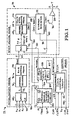
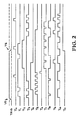
- Fig. 1 shows an apparatus 10 for generating a plurality of digital timing waveforms indicated generally as T on a plurality of output lines shown generally at 12. These timing waveforms T are generated in response to a triggering signal TRIG on an input line 14. As indicated in Fig. 2, the present invention will be described based on producing twelve timing waveforms T0-T11 on twelve parallel output lines 12 respectively; however, the principles of the present invention may be used to generate any number of timing waveforms T on any number of lines 12, in parallel or in series. Furthermore, Fig. 2 shows only one example of the many different timing waveforms T0-T11 that may be generated by the apparatus 10, as will be further described below.
- Fig. 2 shows in solid lines one polarity of the signal TRIG and in dotted lines another polarity of the signal TRIG. For each polarity of the signal TRIG there is a leading edge LE and a trailing edge TE. As will be described below, the apparatus 10 may respond to either polarity of the signal TRIG, with the leading edge LE commencing the generation of the timing waveforms T0-T11. In addition, Fig. 2 shows the timing waveforms T0-T11 as continuing to be generated subsequent to the occurrence of the trailing edge TE; however, the apparatus 10 may respond to the latter to inhibit further generation of the timing waveforms T0-T11.
- the apparatus 10 is a programmable event generator 16 in which each pulse of the timing waveforms T0-T11 corresponds to an event that should occur in an overall system (not shown) in which the generator 16 might be used.
- the generator 16 includes state machine means shown generally at 18 for outputting the timing waveforms T0-T11 on line 12, together with control means shown generally at 20 for controlling the state machine means 18 in response to the signal TRIG on line 14 to output the timing waveforms T0-T11.
- the programmable event generator 16 also includes initialization means shown generally at 22 and coupled to the state machine means 18 for initializing the outputting of the timing waveforms T0-T11.
- the state machine means 18 has an addressable memory 24, such as a programmable read only memory (PROM) 26, for storing a plurality of words W.
- the PROM 26 may store thirty-two words W, each of 18-bit length.
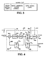
- Fig. 3 shows the content of each word W, which includes a data word DW of twelve bits, a next address word NAW of five bits and a stop word SW of one bit.
- the twelve bits of the data word DW correspond, respectively, to the twelve timing waveforms T0-T11 produced on the parallel output lines 12.
- the next address word NAW defines an address to any other of the words W that is stored in the PROM 26.
- the stop word SW if at one logic level, e.g., logic 1, is used to stop or inhibit the generation of the timing waveforms T0-T11, as will be further described.
- the trailing edge TE of the signal TRIG may be used to so inhibit the timing waveforms T0-T11.
- each data word DW and next address word NAW are read from the PROM 26 on output lines 28, while the stop word SW is read from the PROM 26 on an output line 30.
- a storage register 32 is coupled to the lines 28 to receive and temporarily store the data word DW and next address word NAW of any one word W stored in the PROM 26.
- the storage register 32 is clocked by an internal clock ICLK on a line 34 to output the data word DW on twelve parallel lines 36 that are coupled to the lines 12 via a similar number of output drivers 38, respectively.
- the storage register 32 also outputs the next address word NAW on lines 40 to address another of the words W stored in the PROM 26.
- One reason for using the storage register 32 is to provide registered or "glitch-free" outputs on lines 36 and lines 40. However, if such glitch-free outputs are not necessary, the storage register 32 need not be used, with each data word DW being clocked directly from the PROM 26 onto lines 36 along with each next address word NAW onto lines 40.
- the state machine means 18 also includes a multiplexer 42 having an address input coupled to the lines 40 to receive the next address word NAW, another address input coupled to lines 44 to receive a starting address word SAW from the initialization means 22, and an output coupled to lines 46 which are coupled to an address decoder 48.
- the multiplexer 42 also has a select input coupled to a line 50 carrying a signal MUXSEL.
- the multiplexer 42 responds to the signal MUXSEL to couple either lines 40 or lines 44 to lines 46, whereby lines 46 carry either a starting address word SAW or a next address word NAW, as will be further described.
- the address decoder 48 decodes the starting address word SAW or the next address word NAW on lines 46 to access a word W stored in PROM 26, which is then read onto lines 28 and line 30.
- the multiplexer 42 will first couple lines 44 to lines 46, whereby address decoder 48 will decode a "start address" defined by the SAW to access a first or starting word W in the PROM 26. Then, as the storage register 32 is clocked by a pulse of the internal clock ICLK on line 34, the next address word NAW and the data word DW are temporarily stored in the storage register 32 via lines 28, with the stop word SW being outputted on line 30. Thus, the data word DW of this first word W is outputted onto lines 36 and driven onto lines 12, whereby respective pulses of the timing waveforms T0-T11 are produced in accordance with the logic 1 or logic 0 state of the twelve bits of the data word DW.
- next address word NAW is fed back over lines 40 to the multiplexer 42, which has now been set with the signal MUXSEL on line 50 to couple lines 40 to lines 46. Therefore, the address decoder 48 now decodes the next address word NAW to access another word W stored in the PROM 26. Then, upon the next clock pulse of the internal clock ICLK, this other word W is read from the PROM 26, so that the corresponding next address word NAW and data word DW are temporarily stored in the storage register 36 while the stop word SW is provided on line 30. Consequently, for this next pulse of the internal clock ICLK, pulses of the timing waveforms T0-T11 are produced on lines 12 via drivers 38 in accordance with the logic 1 or logic 0 of the bits of the data word DW.
- next address word NAW is fed back via lines 40 and coupled through the multiplexer 42 onto lines 46 to repeat the process by accessing another word W. This process continues, until the stop word SW of, for example, a logic 1 is produced on line 30, or until the trailing edge TE of the signal TRIG is provided on line 14, as will be further described.
- the control means 20 includes a programmable trigger polarity circuit 52 which receives the signal TRIG on line 14 and, in response, produces any one of several control signals on an output line 54.
- the circuit 52 has a polarity fuse F1 and a stop-trig fuse F2. If not "blown", the fuse F1 will enable the circuit to respond to the leading edge LE of one polarity of the signal TRIG, while if blown or programmed, the fuse F1 will enable the circuit 52 to respond to the leading edge LE of the other polarity of the signal TRIG.
- the stop-trig fuse F2 if blown, will enable the circuit 52 to respond to the trailing edge TE of the signal TRIG to inhibit the generation of the timing waveforms T0-T11; otherwise, the trailing edge TE has no effect.
- the circuit 52 in response to the leading edge LE of the signal TRIG, also produces a latch enable signal on an output line 56 for use as will be described below.
- the control means 20 also includes a control logic circuit 58 having an input coupled to the line 30 carrying the stop word SW, an input coupled to the line 34 carrying the internal clock ICLK, and an input coupled to the line 54 carrying the control signals produced by the trigger polarity circuit 52.
- the control logic circuit 58 is used to generate the signal MUXSEL on the line 50 and a signal START/STOP on a line 60.
- the control logic circuit 58 has a flip-flop FF1 which responds to the control signals on line 54 or the stop word SW on line 30 to produce the signal START/STOP on line 60, while another flip-flop FF2 is clocked by the internal clock ICLK on line 34 to produce a logic 1 signal MUXSEL on line 50, as will be further described.
- a programmable clock control circuit 62 is controlled by the signal START/STOP on line 60 to produce the internal clock ICLK on line 34.
- the clock control circuit 62 has two inputs coupled to respective lines CLK/X1 and X2 for receiving either an external reference clock CLK on line CLK/X1 or on external reference clock from a crystal (not shown) coupled across lines CLK/X1, and X2, from which the internal clock ICLK is produced.
- the programmable clock control circuit 62 is coupled to an external capacitor over a line 64 and may output a system clock CLKOUT on an output line 66 to provide system timing for an overall system (not shown) in which the programmable event generator 16 might be used.
- the programmable trigger polarity circuit 52 in response to the leading edge LE of the signal TRIG, produces a control signal on line 54 and the latch enable signal on line 56.
- the flip-flop FF1 of the control logic circuit 58 will produce the signal START/STOP, e.g., a logic 1, on line 60, whereby the programmable clock control circuit 62 will then be enabled to provide the internal clock ICLK on line 34, as well as the signal CLKOUT on line 66.
- the flip-flop FF2 of the control logic circuit 58 will clock in a logic 1 to produce a logic 1 signal MUXSEL on line 50.
- the flip-flop FF1 of the control logic circuit 58 will produce the signal START/STOP, e.g., logic 0, on line 60 to stop the generation of the internal clock ICLK in response to the logic 1 stop word SW on line 30.
- the programmable trigger polarity circuit 52 will respond to the trailing edge TE of the signal TRIG to produce a control signal on line 54, whereby the flip-flip FF1 will respond to produce the signal START/STOP of logic 0 to inhibit the internal clock ICLK.
- the initialization means 22 has a latch 68 for latching an externally received address of, for example, three bit length A0-A2 over three respective lines 70.
- the latch 68 latches the external address A0-A2 in response to the latch enable signal on line 56 and outputs this latched address over three lines 72 to an address decoder 74.
- An addressable memory 76 such as a mapping programmable read only memory or PROM 78, is used for storing a number of starting address words SAW that may be read onto the lines 44.
- the mapping PROM 76 may be an 8 x 5 mapping PROM 78 for storing eight starting address words SAW each of 5-bit length.
- the latch 68 In the operation generally of the initialization means 22, when a given external address A0-A2 is received on the lines 70, the latch 68 outputs this address A0-A2 onto lines 72. Consequently, the address decoder 74 decodes this address A0-A2 to access a specified starting address word SAW in the PROM 76, whereby this SAW is then read onto lines 44.
- the state machine PROM 26 has been programmed with up to thirty-two words W
- the mapping PROM 78 has been programmed with up to eight starting address words SAW
- the programmable trigger polarity circuit 52 has been programmed to respond to the leading edge LE of the signal TRIG of the desired polarity, but has not been programmed to respond to the trailing edge TE of the signal TRIG to inhibit the generation of the timing waveforms T0-T11.
- the programmable clock control circuit 62 has been programmed to produce an internal clock ICLK of, for example, 100 MHz or a 10 ns period in response to the external clock CLK on line CLK/X1.
- the programmable event generator 16 has been reset, so that the signal MUXSEL is a logic 0, whereby the multiplexer 42 is coupling lines 44 to lines 46.
- the external address A0-A2 is supplied on the lines 70 to latch 68, whereby the address decoder 74 decodes this address A0-A2 to access a desired starting address word SAW in the mapping PROM 78. Accordingly, this starting address word SAW is read onto lines 44 and, via multiplexer 42, onto lines 46, so that address decoder 48 at this time decodes this SAW to access one of the thirty-two words W stored in the PROM 26.
- the signal TRIG is supplied to the programmable trigger polarity circuit 52.
- the latch enable signal on line 56 is produced to latch the external address A0-A2 in latch 68. This latching stabilizes the stored address A0-A2, so that a stabilized starting address word SAW is read from the PROM 78, resulting in a stabilized word W being read from the PROM 26.
- the programmable trigger polarity circuit 52 produces a control signal on line 54 that is stored in the flip-flop FF1, resulting in a logic 1 signal START/STOP on line 60 being generated.
- the programmable clock control circuit 62 In response to the logic 1 signal START/STOP, the programmable clock control circuit 62 produces the internal clock ICLK on the line 34, which then clocks the storage register 32, whereby the timing waveforms T0-T11 begin to be generated pursuant to the data word DW currently stored in the register 32.
- the internal clock ICLK also is fed back to the control logic circuit 58 to clock the logic 1 into the flip-flop FF2, so that the logic 1 signal MUXSEL is produced on the line 50 to set the multiplexer 42. Therefore, now the multiplexer 42 couples the next address word NAW on the lines 40 to the lines 46.
- the programmable trigger polarity circuit 52 if so programmed, the occurrence of the trailing edge TE of the signal TRIG results in a control signal on line 54 being generated, whereby in response the flip-flop FF1 produces the logic 0 signal START/STOP to inhibit the internal clock ICLK.
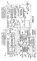
- Fig. 4 shows a more detailed block diagram of one embodiment of the programmable clock control circuit 62.
- This circuit 62 includes a portion of a phase locked loop 80 that responds to, for example, the externally applied clock CLK on line CLK/X1 to produce a frequency signal on a line 82.
- the phase locked loop 80 has a voltage controlled oscillator 84 producing the frequency signal on line 82 and which is, for example, designed to run at a nominal frequency of 100 MHz.
- the phase locked loop 80 also has, for example, a programmable multiplication factor of 5 or 10 which is provided by programming a feedback divider 86 to divide by 5 or 10.
- the divider 86 will be programmed to divide the 100 MHz signal on line 82 by 10, to output on a line 88 a 10 MHz signal that is phase compared with the 10 MHz signal on line CLK/X1 by a phase comparator 90 in accordance with conventional phase locked loop principles. If the external clock CLK is at 20 MHz, the divider 86 will be programmed to divide the 100 MHz signal on line 82 by 5, to output on line 88 a 20 MHz signal for phase comparison purposes.
- the divider 86 may be programmed by providing a fuse F3 which is blown or not blown, depending on the desired multiplication factor.
- the programmable clock control circuit 62 also has a programmable divider 92 which divides the 100 MHz signal on line 82 to produce the internal clock ICLK on the line 34.
- the programmable divider 88 can have two fuses F4 and F5 which, if blown or not, will cause the divider 88 to divide the 100 MHz signal on line 82 by 1 of 4 values.
- the programmable clock control circuit 62 has a programmable divider 94 for dividing the 100 MHz signal on line 82 to produce the signal CLKOUT on line 66.
- the divider 94 has a fuse F6 to divide the 100 MHz signal on line 82 by 5 or 10. If the fuse F6 is not blown, the divider 94 will, for example, divide by 5 to output on the line 66 the signal CLKOUT of 20 MHz, whereas, if the fuse F6 is blown, the divider 94 will divide by 10 to produce the signal CLKOUT of 10 MHz.
- a portion of the phase locked loop 80 is externally coupled over the line 64 to drive the VCO 84 via a filter 96.
- the reason for this external connection of the capacitor C is that the overall programmable event generator 16 can be implemented as an integrated circuit, but for conventional reasons it is possible, but not advantageous, to include the capacitor C as part of the integrated circuit.
- the programmable event generator 16 typically may be manufactured and sold to a user in an unprogrammed state. That is, the PROM 26 and the PROM 78 will not be programmed with the words W and starting address words SAW, nor will the fuses F1-F6 be blown. The user may then program the PROM 26 and the PROM 78, as well as selectively blow the fuses F1-F6 to configure the programmable event generator 16 and generate the timing waveforms T0-T11, as desired.
- Fig. 5 shows the same programmable event generator 16 as in Fig. 1, except that the generator 16 also may be manufactured and sold with a test PROM 26' and associated address decoder 48', coupled to lines 28, 30 and lines 46 as shown, bypassing the PROM 26 and address decoder 48.
- the generator 16 also then has a test mapping PROM 78' and corresponding address decoder 74' coupled to lines 44 and lines 72 as shown, bypassing the mapping PROM 78 and address decoder 74.
- the purpose of providing these additional components is to test the programmable event generator 16 by simulating, prior to programming, the operation of the generator 16 as if it had been programmed as described above. Two tests that may be performed are a functional test of the overall programmable event generator 16 and a high-frequency test of the phase-locked loop 80, as will now be described.
- the test PROM 26' may, for example, be programmed with six test words W' (not shown) each of 18-bit length having a 12-bit data word DW', a 5-bit next address word NAW' and a 1-bit stop word SW', in which one stop word SW' has a logic 1.
- the test mapping PROM 78' may, for example, be programmed with two starting address words SAW' (not shown) each of 3-bit length.
- a relatively slow clock is used on line CLK/X1 to bypass the phase-locked loop 80 (see Fig. 4) and, thereby, provide a slow internal clock ICLK on line 34.
- one bit of the external address A0-A2, e.g, bit A0, is provided on lined 70 at a very high voltage to drive off the address decoder 74 and mapping PROM 78, while bits A1-A2 are in their normal voltage state to address the test mapping PROM 78' via the address decoder 74'.
- test timing waveforms T'0-T'11 (not shown) can be detected.
- the logic 1 stop word SW' is produced on line 30, this operation of the programmable event generator 16 will stop.
- phase-locked loop operates at a high frequency, e.g., 100 MHz. Therefore, to test this high-frequency operation, a crystal (not shown) of appropriate frequency is coupled to lines CLK/X1 and X2. Then, the signal CLKOUT may be detected to determine if proper frequency multiplication is being performed by the phase-locked loop 80.
- overall high-frequency operation of the programmable event generator 16 can be tested by again supplying the external address A0-A2 on lines 70 with bit A0 at a very high voltage and supplying the signal TRIG to line 14, whereby the test timing waveforms T'0-T'11 outputted on lines 12 can be detected.
Landscapes
- Engineering & Computer Science (AREA)
- Theoretical Computer Science (AREA)
- Physics & Mathematics (AREA)
- General Engineering & Computer Science (AREA)
- General Physics & Mathematics (AREA)
- Tests Of Electronic Circuits (AREA)
- Test And Diagnosis Of Digital Computers (AREA)
- Pulse Circuits (AREA)
- Manipulation Of Pulses (AREA)
- Magnetic Resonance Imaging Apparatus (AREA)
- Electrophonic Musical Instruments (AREA)
- Read Only Memory (AREA)
- Details Of Television Scanning (AREA)
- Stabilization Of Oscillater, Synchronisation, Frequency Synthesizers (AREA)
- Signal Processing For Digital Recording And Reproducing (AREA)
Claims (16)
- Schaltung zum Erzeugen einer Folge digitaler Zeitsteuerungswellenformen (T), von denen jede in Form eines binären Datenwortes (DW) vorliegt, an einem Ausgang (12) als Antwort auf ein Triggersignal (TRIG), mit:
einer Speichereinrichtung (24) zum Speichern der Datenwörter in jeweiligen Adressen;
einer Ausgabeeinrichtung (32) zum Ausgeben der Datenwörter als Zeitsteuerungswellenformen (T) von der Speichereinrichtung an den Ausgang;
einer Adressiereinrichtung (48) zum Adressieren eines an die Ausgabeeinrichtung zu übertragenden gespeicherten Datenwortes in der Speichereinrichtung;
einer Starteinrichtung (22), die so auf eine extern zugeführte Adresse reagiert, daß sie mit einem Startadreßwort (SAW) ein erstes Datenwort in der Folge zum Erscheinen in der Speichereinrichtung wählt; und
einer Steuereinrichtung (20), die so auf das Triggersignal und ein externes Taktsignal (CLK/X) reagiert, daß sie Start- und Stoppsignale für die Ausgabe der Folge erzeugt, und daß sie die Ausgabe der Folge aus der Ausgabeeinrichtung steuert;
dadurch gekennzeichnet,
daß die Speichereinrichtung so ausgelegt ist, daß sie ein Adreßwort (NAW) des nächsten Datenwortes in der Folge getrennt von, jedoch in Assoziation mit dem Inhalt (DW) der digitalen Wellenform an jeder der jeweiligen Adressen speichert, und daß eine Selektionseinrichtung (42) vorgesehen ist, die als Antwort auf ein Selektionssteuersignal (MUXSEL) von der Steuereinrichtung der Adressiereinrichtung anfangs die Startadresse und anschließend die Adresse des nächsten Datenwortes in der Folge zuführt. - Schaltung nach Anspruch 1, dadurch gekennzeichnet, daß die Ausgabeeinrichtung ein Speicherregister aufweist, das so ausgelegt ist, daß es ein Datenwort und die zugehörige Adresse des nächsten Wortes in der Folge von der Speichereinrichtung empfängt, und das Datenwort dem Ausgang sowie die Adresse der Selektionseinrichtung zuführt.
- Schaltung nach Anspruch 1 oder 2, dadurch gekennzeichnet, daß die digitalen Zeitsteuerungswellenformen (T) in Synchronisation mit dem Triggersignal (TRIG) erzeugt werden.
- Schaltung nach Anspruch 1, 2 oder 3, dadurch gekennzeichnet, daß das Triggersignal (TRIG) eine bestimmte Wellenform hat und die digitalen Zeitsteuerungswellenformen (T) nicht notwendigerweise der Wellenform des Triggersignals (TRIG) ähnlich sind.
- Schaltung nach einem der vorhergehenden Ansprüche, dadurch gekennzeichnet, daß die Speichereinrichtung (24) einen programmierbaren Nurlesespeicher (26) aufweist.
- Schaltung nach einem der vorhergehenden Ansprüche, dadurch gekennzeichnet, daß die Starteinrichtung (22) aufweist:
einen adressierbaren Speicher (78) zum Speichern und Ausgeben eines Wortes von der Vielzahl derartiger Startadreßwörter (SAW), und
eine Einrichtung (74) zum Empfangen und Dekodieren eines extern zugeführten Adreßwortes (A₀,A₁,A₂) zum Zugreifen auf den adressierbaren Speicher, um ein Wort der Vielzahl von Startadreßwörtern an die Selektionseinrichtung auszugeben. - Schaltung nach einem der vorhergehenden Ansprüche, dadurch gekennzeichnet, daß die Steuereinrichtung (20) aufweist:
eine Einrichtung (58) zum Erzeugen eines Startsignals als Antwort auf das Triggersignal (TRIG); und
eine Einrichtung (62) zum Erzeugen eines Taktsignals (ICLK) zum Takten der Speicher- und der Ausgabeeinrichtung (24,32) als Antwort auf das Startsignal. - Schaltung nach einem der Ansprüche 1 bis 6, dadurch gekennzeichnet, daß das Triggersignal (TRIG) eine Vorderflanke und eine Hinterflanke hat und daß die Steuereinrichtung (20) aufweist:
eine Einrichtung (58), die das Startsignal als Antwort auf die Vorderflanke und das Stoppsignal als Antwort auf die Hinterflanke erzeugt; und
eine Einrichtung (62), die zum Takten der Speicher- und der Ausgabeeinrichtung (24,32) ein Taktsignal (ICLK) als Antwort auf das Startsignal erzeugt, und die das Taktsignal (ICLK) als Antwort auf das Stoppsignal verhindert. - Schaltung nach einem der vorhergehenden Ansprüche, dadurch gekennzeichnet, daß mindestens ein Stoppwort (SW) als letztes Datenwort in der Folge an einer Adresse in der Speichereinrichtung gespeichert wird, und daß die Speichereinrichtung (20) die Speicher- und die Ausgabeeinrichtung (24,32) als Antwort auf das Stoppwort (SW) so steuert, daß diese die Zufuhr von Datenwörtern an den Ausgang verhindern.
- Schaltung nach einem der vorhergehenden Ansprüche, dadurch gekennzeichnet, daß die Steuereinrichtung (20) eine programmierbare Einrichtung (62) aufweist, die zum Takten der Speicher- und der Ausgabeeinrichtung (24,32) ein Taktsignal (ICLK) mit einer Selektionsfrequenz erzeugt.
- Schaltung nach Anspruch 10, sofern abhängig von Anspruch 8, dadurch gekennzeichnet, daß die programmierbare Einrichtung auf das Startsignal hin das Taktsignal aktiviert und auf das Stoppsignal hin das Taktsignal verhindert.
- Schaltung nach einem der vorhergehenden Ansprüche, gekennzeichnet durch eine Halteeinrichtung (68) zum zeitweiligen Halten der Startadresse.
- Schaltung nach Anspruch 12, dadurch gekennzeichnet, daß die Halteeinrichtung eine Latch-Schaltung aufweist.
- Schaltung nach Anspruch 12 oder 13, dadurch gekennzeichnet, daß die Steuereinrichtung enthält:
eine auf die Vorderflanke des Triggersignals (TRIG) reagierende Triggerschaltungseinrichtung (52) zum Erzeugen eines ersten Signals zur Aktivierung der Halteeinrichtung (68) und zum Erzeugen eines zweiten Signals; und
eine Steuerlogikschalteinrichtung (58) zum Erzeugen des Selektionssteuersignals und des Startsignals als Antwort auf das zweite Signal. - Schaltung nach Anspruch 14, dadurch gekennzeichnet, daß die Triggerschaltungseinrichtung (52) programmierbar ist zum Erzeugen eines dritten Signals als Antwort auf die Hinterflanke des Triggersignals, und daß die Steuerlogikschalteinrichtung (58) das Stoppsignal als Antwort auf das dritte Signal erzeugt.
- Schaltung nach einem der Ansprüche 14 oder 15, dadurch gekennzeichnet, daß das Triggersignal (TRIG) die eine oder eine andere Polarität hat, und daß die Triggerschaltungseinrichtung programmierbar ist zum Reagieren auf jede der beiden Polaritäten des Triggersignals.
Priority Applications (1)
| Application Number | Priority Date | Filing Date | Title |
|---|---|---|---|
| AT85304842T ATE69658T1 (de) | 1984-07-09 | 1985-07-08 | Geraet zur erzeugung digitaler taktimpulsfunktionen. |
Applications Claiming Priority (2)
| Application Number | Priority Date | Filing Date | Title |
|---|---|---|---|
| US628707 | 1984-07-09 | ||
| US06/628,707 US4719593A (en) | 1984-07-09 | 1984-07-09 | Apparatus for generating digital timing waveforms |
Publications (3)
| Publication Number | Publication Date |
|---|---|
| EP0168232A2 EP0168232A2 (de) | 1986-01-15 |
| EP0168232A3 EP0168232A3 (en) | 1988-05-25 |
| EP0168232B1 true EP0168232B1 (de) | 1991-11-21 |
Family
ID=24519985
Family Applications (1)
| Application Number | Title | Priority Date | Filing Date |
|---|---|---|---|
| EP85304842A Expired - Lifetime EP0168232B1 (de) | 1984-07-09 | 1985-07-08 | Gerät zur Erzeugung digitaler Taktimpulsfunktionen |
Country Status (5)
| Country | Link |
|---|---|
| US (1) | US4719593A (de) |
| EP (1) | EP0168232B1 (de) |
| JP (1) | JPS6145625A (de) |
| AT (1) | ATE69658T1 (de) |
| DE (1) | DE3584696D1 (de) |
Families Citing this family (54)
| Publication number | Priority date | Publication date | Assignee | Title |
|---|---|---|---|---|
| GB2196450B (en) * | 1986-10-20 | 1991-02-13 | Mars Inc | Data-storing tokens |
| JPS63131616A (ja) * | 1986-11-20 | 1988-06-03 | Mitsubishi Electric Corp | プログラマブルクロツク分周器 |
| US5133064A (en) * | 1987-04-27 | 1992-07-21 | Hitachi, Ltd. | Data processing system generating clock signal from an input clock, phase locked to the input clock and used for clocking logic devices |
| US4958277A (en) * | 1987-07-24 | 1990-09-18 | Motorola, Inc. | Queued serial peripheral interface for use in a data processing system |
| US5349544A (en) * | 1988-06-15 | 1994-09-20 | Advanced Micro Devices, Inc. | Programmable system synchronizer |
| US5185880A (en) * | 1989-06-05 | 1993-02-09 | Matsushita Electric Industrial Co., Ltd. | Stored instructions executing type timing signal generating system |
| US4956798A (en) * | 1989-08-03 | 1990-09-11 | Tektronix, Inc. | Arbitrary waveform generator with adjustable spacing |
| GB2252432B (en) * | 1991-02-01 | 1994-09-28 | Intel Corp | Method and apparatus for operating a computer bus using selectable clock frequencies |
| WO1993025954A2 (en) * | 1992-06-11 | 1993-12-23 | Sierra Semiconductor Corporation | A universal programming interface for clock generators |
| US5734877A (en) * | 1992-09-09 | 1998-03-31 | Silicon Graphics, Inc. | Processor chip having on-chip circuitry for generating a programmable external clock signal and for controlling data patterns |
| JP2907033B2 (ja) * | 1994-11-24 | 1999-06-21 | 横河電機株式会社 | タイミング信号発生装置 |
| US5744991A (en) | 1995-10-16 | 1998-04-28 | Altera Corporation | System for distributing clocks using a delay lock loop in a programmable logic circuit |
| EP0825506B1 (de) * | 1996-08-20 | 2013-03-06 | Invensys Systems, Inc. | Verfahren und Gerät zur Fernprozesssteuerung |
| US7441254B1 (en) | 1997-07-09 | 2008-10-21 | International Business Machines Corporation | Simulation of memory-mapped I/O |
| WO1999059247A1 (de) * | 1998-05-11 | 1999-11-18 | Infineon Technologies Ag | Zeitgabevorrichtung und zeitgabeverfahren |
| US6691183B1 (en) | 1998-05-20 | 2004-02-10 | Invensys Systems, Inc. | Second transfer logic causing a first transfer logic to check a data ready bit prior to each of multibit transfer of a continous transfer operation |
| US6346827B1 (en) | 1998-09-09 | 2002-02-12 | Altera Corporation | Programmable logic device input/output circuit configurable as reference voltage input circuit |
| US6483886B1 (en) | 1999-01-08 | 2002-11-19 | Altera Corporation | Phase-locked loop circuitry for programmable logic devices |
| US6252419B1 (en) | 1999-01-08 | 2001-06-26 | Altera Corporation | LVDS interface incorporating phase-locked loop circuitry for use in programmable logic device |
| US6218876B1 (en) | 1999-01-08 | 2001-04-17 | Altera Corporation | Phase-locked loop circuitry for programmable logic devices |
| US6177844B1 (en) | 1999-01-08 | 2001-01-23 | Altera Corporation | Phase-locked loop or delay-locked loop circuitry for programmable logic devices |
| JP3352080B2 (ja) * | 1999-01-08 | 2002-12-03 | 株式会社アドバンテスト | 波形発生装置 |
| US6472903B1 (en) | 1999-01-08 | 2002-10-29 | Altera Corporation | Programmable logic device input/output architecture with power bus segmentation for multiple I/O standards |
| US7089530B1 (en) * | 1999-05-17 | 2006-08-08 | Invensys Systems, Inc. | Process control configuration system with connection validation and configuration |
| US7272815B1 (en) | 1999-05-17 | 2007-09-18 | Invensys Systems, Inc. | Methods and apparatus for control configuration with versioning, security, composite blocks, edit selection, object swapping, formulaic values and other aspects |
| WO2000070417A1 (en) * | 1999-05-17 | 2000-11-23 | The Foxboro Company | Process control configuration system with parameterized objects |
| US7096465B1 (en) | 1999-05-17 | 2006-08-22 | Invensys Systems, Inc. | Process control configuration system with parameterized objects |
| US6754885B1 (en) | 1999-05-17 | 2004-06-22 | Invensys Systems, Inc. | Methods and apparatus for controlling object appearance in a process control configuration system |
| US6501995B1 (en) | 1999-06-30 | 2002-12-31 | The Foxboro Company | Process control system and method with improved distribution, installation and validation of components |
| US6788980B1 (en) | 1999-06-11 | 2004-09-07 | Invensys Systems, Inc. | Methods and apparatus for control using control devices that provide a virtual machine environment and that communicate via an IP network |
| US6510352B1 (en) | 1999-07-29 | 2003-01-21 | The Foxboro Company | Methods and apparatus for object-based process control |
| US6564334B1 (en) | 1999-12-01 | 2003-05-13 | Zilog, Inc. | Programmable output generator |
| US6473660B1 (en) | 1999-12-03 | 2002-10-29 | The Foxboro Company | Process control system and method with automatic fault avoidance |
| US6779128B1 (en) | 2000-02-18 | 2004-08-17 | Invensys Systems, Inc. | Fault-tolerant data transfer |
| ES2169670B1 (es) * | 2000-05-30 | 2003-09-01 | Univ Pais Vasco | Generador digital programable de señales. |
| US7242991B2 (en) * | 2002-04-15 | 2007-07-10 | Invensys Systems, Inc. | Workflow control configurator for use with process, factory-floor, environmental, computer aided manufacturing-based or other control system |
| US6832173B1 (en) | 2002-07-30 | 2004-12-14 | Altera Corporation | Testing circuit and method for phase-locked loop |
| US7010376B2 (en) * | 2002-10-25 | 2006-03-07 | Pulp And Paper Research Institute Of Canada | Diagnostic for poorly tuned control loops |
| ES2211353B1 (es) * | 2002-12-20 | 2005-09-16 | Universidad De Sevilla | Procedimiento para la induccion de valores en los registros de un circuito digital emulado mediante un circuito integrado de emulacion hardware. |
| US6867616B1 (en) | 2003-06-04 | 2005-03-15 | Altera Corporation | Programmable logic device serial interface having dual-use phase-locked loop circuitry |
| US7019570B2 (en) * | 2003-09-05 | 2006-03-28 | Altera Corporation | Dual-gain loop circuitry for programmable logic device |
| US6924678B2 (en) * | 2003-10-21 | 2005-08-02 | Altera Corporation | Programmable phase-locked loop circuitry for programmable logic device |
| US7091760B1 (en) | 2004-02-25 | 2006-08-15 | Altera Corporation | DLL with adjustable phase shift using processed control signal |
| US7073629B2 (en) * | 2004-02-26 | 2006-07-11 | The Boeing Company | Ladder support apparatus and methods |
| US7761923B2 (en) * | 2004-03-01 | 2010-07-20 | Invensys Systems, Inc. | Process control methods and apparatus for intrusion detection, protection and network hardening |
| US7075365B1 (en) | 2004-04-22 | 2006-07-11 | Altera Corporation | Configurable clock network for programmable logic device |
| US7230495B2 (en) | 2004-04-28 | 2007-06-12 | Micron Technology, Inc. | Phase-locked loop circuits with reduced lock time |
| US7436228B1 (en) | 2005-12-22 | 2008-10-14 | Altera Corporation | Variable-bandwidth loop filter methods and apparatus |
| WO2007123753A2 (en) | 2006-03-30 | 2007-11-01 | Invensys Systems, Inc. | Digital data processing apparatus and methods for improving plant performance |
| US7728674B1 (en) | 2006-05-19 | 2010-06-01 | Altera Corporation | Voltage-controlled oscillator methods and apparatus |
| CN104407518B (zh) | 2008-06-20 | 2017-05-31 | 因文西斯系统公司 | 对用于过程控制的实际和仿真设施进行交互的系统和方法 |
| US8463964B2 (en) * | 2009-05-29 | 2013-06-11 | Invensys Systems, Inc. | Methods and apparatus for control configuration with enhanced change-tracking |
| US8127060B2 (en) * | 2009-05-29 | 2012-02-28 | Invensys Systems, Inc | Methods and apparatus for control configuration with control objects that are fieldbus protocol-aware |
| JP5637871B2 (ja) | 2011-01-13 | 2014-12-10 | 株式会社椿本チエイン | コンベヤチェーン |
Family Cites Families (14)
| Publication number | Priority date | Publication date | Assignee | Title |
|---|---|---|---|---|
| US3689914A (en) * | 1971-08-09 | 1972-09-05 | Rca Corp | Waveform generator |
| US3763364A (en) * | 1971-11-26 | 1973-10-02 | North American Rockwell | Apparatus for storing and reading out periodic waveforms |
| DE2524759A1 (de) * | 1975-06-04 | 1976-12-16 | Anker Werke Ag | Einrichtung zur erzeugung unterschiedlicher taktbilder |
| DE2738352A1 (de) * | 1977-08-23 | 1979-03-01 | Siemens Ag | Funktionsgenerator mit speichermatrix |
| US4168527A (en) * | 1978-02-17 | 1979-09-18 | Winkler Dean A | Analog and digital circuit tester |
| FR2417892A1 (fr) * | 1978-02-21 | 1979-09-14 | Materiel Telephonique | Multigenerateur de sequences a evolutions modifiables par programmation |
| US4198683A (en) * | 1978-05-01 | 1980-04-15 | Tektronix, Inc. | Multiple waveform storage system |
| US4222108A (en) * | 1978-12-01 | 1980-09-09 | Braaten Norman J | Digitally-programmed arbitrary waveform generator |
| FR2450006A1 (fr) * | 1979-02-22 | 1980-09-19 | Materiel Telephonique | Dispositif generateur sequentiel de signaux numeriques conditionnel et programmable |
| JPS55134898A (en) * | 1979-04-05 | 1980-10-21 | Sony Corp | Digital waveform gneration circuit |
| US4404644A (en) * | 1980-05-22 | 1983-09-13 | Barr & Stroud Limited | Waveform generator |
| EP0054159A3 (de) * | 1980-12-15 | 1982-07-28 | BURROUGHS CORPORATION (a Michigan corporation) | Programmierbarer Zeitsteuerungsimpulsgeber |
| US4456890A (en) * | 1982-04-05 | 1984-06-26 | Computer Peripherals Inc. | Data tracking clock recovery system using digitally controlled oscillator |
| US4513387A (en) * | 1982-07-13 | 1985-04-23 | Lgz Landis & Gyr Zug Ag | Method and an apparatus for generating periodic digital time function signals |
-
1984
- 1984-07-09 US US06/628,707 patent/US4719593A/en not_active Expired - Lifetime
-
1985
- 1985-07-08 JP JP60151195A patent/JPS6145625A/ja active Granted
- 1985-07-08 AT AT85304842T patent/ATE69658T1/de not_active IP Right Cessation
- 1985-07-08 EP EP85304842A patent/EP0168232B1/de not_active Expired - Lifetime
- 1985-07-08 DE DE8585304842T patent/DE3584696D1/de not_active Expired - Lifetime
Also Published As
| Publication number | Publication date |
|---|---|
| JPH0535925B2 (de) | 1993-05-27 |
| EP0168232A2 (de) | 1986-01-15 |
| DE3584696D1 (de) | 1992-01-02 |
| EP0168232A3 (en) | 1988-05-25 |
| ATE69658T1 (de) | 1991-12-15 |
| US4719593A (en) | 1988-01-12 |
| JPS6145625A (ja) | 1986-03-05 |
Similar Documents
| Publication | Publication Date | Title |
|---|---|---|
| EP0168232B1 (de) | Gerät zur Erzeugung digitaler Taktimpulsfunktionen | |
| US5109506A (en) | Microcomputer system including a microprocessor reset circuit | |
| US7629822B2 (en) | Delay locked loop in semiconductor memory device and method for generating divided clock therein | |
| US5991888A (en) | Test clock modes | |
| US6920080B2 (en) | Methods for generating output control signals in synchronous semiconductor memory devices and related semiconductor memory devices | |
| US7030674B2 (en) | Multiphase clock generators | |
| JP4480471B2 (ja) | レジスタ制御遅延固定ループ | |
| US5990715A (en) | Semiconductor integrated circuit using a synchronized control signal | |
| US6917660B2 (en) | Adaptive de-skew clock generation | |
| US7154311B2 (en) | Delay locked loop in semiconductor memory device and locking method thereof | |
| US6330197B1 (en) | System for linearizing a programmable delay circuit | |
| US6472913B2 (en) | Method and apparatus for data sampling | |
| US4737792A (en) | Counter-based simulated target generator | |
| JPH023210B2 (de) | ||
| JPH0650338B2 (ja) | テスト装置 | |
| WO1993025954A2 (en) | A universal programming interface for clock generators | |
| US4553100A (en) | Counter-address memory for multi-channel timing signals | |
| JP2000132265A (ja) | クロックを変えて動作できるマイクロプロセッサ | |
| JP3479389B2 (ja) | データ処理システム及び半導体集積回路 | |
| US5621705A (en) | Programmable timing unit for generating multiple coherent timing signals | |
| US5577238A (en) | Multistage timing circuit having multiple counters in each timer for generating programmable duration output signals without any delay | |
| US4726025A (en) | Generation and diagnostic verification of complex timing cycles | |
| US6392404B1 (en) | Triggered integrated circuit tester | |
| US5023822A (en) | Pulse ratio system | |
| US6535457B1 (en) | Semiconductor memory device having clock generator for controlling memory and method of generating clock signal |
Legal Events
| Date | Code | Title | Description |
|---|---|---|---|
| PUAI | Public reference made under article 153(3) epc to a published international application that has entered the european phase |
Free format text: ORIGINAL CODE: 0009012 |
|
| AK | Designated contracting states |
Designated state(s): AT BE CH DE FR GB IT LI LU NL SE |
|
| PUAL | Search report despatched |
Free format text: ORIGINAL CODE: 0009013 |
|
| AK | Designated contracting states |
Kind code of ref document: A3 Designated state(s): AT BE CH DE FR GB IT LI LU NL SE |
|
| 17P | Request for examination filed |
Effective date: 19880518 |
|
| 17Q | First examination report despatched |
Effective date: 19891127 |
|
| PGFP | Annual fee paid to national office [announced via postgrant information from national office to epo] |
Ref country code: LU Payment date: 19910607 Year of fee payment: 7 |
|
| GRAA | (expected) grant |
Free format text: ORIGINAL CODE: 0009210 |
|
| AK | Designated contracting states |
Kind code of ref document: B1 Designated state(s): AT BE CH DE FR GB IT LI LU NL SE |
|
| PG25 | Lapsed in a contracting state [announced via postgrant information from national office to epo] |
Ref country code: SE Effective date: 19911121 Ref country code: NL Effective date: 19911121 Ref country code: LI Effective date: 19911121 Ref country code: CH Effective date: 19911121 Ref country code: BE Effective date: 19911121 Ref country code: AT Effective date: 19911121 |
|
| REF | Corresponds to: |
Ref document number: 69658 Country of ref document: AT Date of ref document: 19911215 Kind code of ref document: T |
|
| ITF | It: translation for a ep patent filed | ||
| REF | Corresponds to: |
Ref document number: 3584696 Country of ref document: DE Date of ref document: 19920102 |
|
| EPTA | Lu: last paid annual fee | ||
| REG | Reference to a national code |
Ref country code: CH Ref legal event code: PL |
|
| ET | Fr: translation filed | ||
| NLV1 | Nl: lapsed or annulled due to failure to fulfill the requirements of art. 29p and 29m of the patents act | ||
| PG25 | Lapsed in a contracting state [announced via postgrant information from national office to epo] |
Ref country code: LU Free format text: LAPSE BECAUSE OF NON-PAYMENT OF DUE FEES Effective date: 19920731 |
|
| PLBE | No opposition filed within time limit |
Free format text: ORIGINAL CODE: 0009261 |
|
| STAA | Information on the status of an ep patent application or granted ep patent |
Free format text: STATUS: NO OPPOSITION FILED WITHIN TIME LIMIT |
|
| 26N | No opposition filed | ||
| REG | Reference to a national code |
Ref country code: GB Ref legal event code: IF02 |
|
| PGFP | Annual fee paid to national office [announced via postgrant information from national office to epo] |
Ref country code: GB Payment date: 20020613 Year of fee payment: 18 |
|
| PGFP | Annual fee paid to national office [announced via postgrant information from national office to epo] |
Ref country code: FR Payment date: 20020702 Year of fee payment: 18 |
|
| PGFP | Annual fee paid to national office [announced via postgrant information from national office to epo] |
Ref country code: DE Payment date: 20020731 Year of fee payment: 18 |
|
| PG25 | Lapsed in a contracting state [announced via postgrant information from national office to epo] |
Ref country code: GB Free format text: LAPSE BECAUSE OF NON-PAYMENT OF DUE FEES Effective date: 20030708 |
|
| PG25 | Lapsed in a contracting state [announced via postgrant information from national office to epo] |
Ref country code: DE Free format text: LAPSE BECAUSE OF NON-PAYMENT OF DUE FEES Effective date: 20040203 |
|
| GBPC | Gb: european patent ceased through non-payment of renewal fee |
Effective date: 20030708 |
|
| PG25 | Lapsed in a contracting state [announced via postgrant information from national office to epo] |
Ref country code: FR Free format text: LAPSE BECAUSE OF NON-PAYMENT OF DUE FEES Effective date: 20040331 |
|
| REG | Reference to a national code |
Ref country code: FR Ref legal event code: ST |