EP0166110B1 - Leiterplattenanordnung - Google Patents
Leiterplattenanordnung Download PDFInfo
- Publication number
- EP0166110B1 EP0166110B1 EP85105125A EP85105125A EP0166110B1 EP 0166110 B1 EP0166110 B1 EP 0166110B1 EP 85105125 A EP85105125 A EP 85105125A EP 85105125 A EP85105125 A EP 85105125A EP 0166110 B1 EP0166110 B1 EP 0166110B1
- Authority
- EP
- European Patent Office
- Prior art keywords
- circuit board
- printed circuit
- components
- insulating material
- board arrangement
- Prior art date
- Legal status (The legal status is an assumption and is not a legal conclusion. Google has not performed a legal analysis and makes no representation as to the accuracy of the status listed.)
- Expired - Lifetime
Links
Images

Classifications
-
- H—ELECTRICITY
- H05—ELECTRIC TECHNIQUES NOT OTHERWISE PROVIDED FOR
- H05K—PRINTED CIRCUITS; CASINGS OR CONSTRUCTIONAL DETAILS OF ELECTRIC APPARATUS; MANUFACTURE OF ASSEMBLAGES OF ELECTRICAL COMPONENTS
- H05K1/00—Printed circuits
- H05K1/02—Details
- H05K1/0213—Electrical arrangements not otherwise provided for
- H05K1/0254—High voltage adaptations; Electrical insulation details; Overvoltage or electrostatic discharge protection ; Arrangements for regulating voltages or for using plural voltages
- H05K1/0256—Electrical insulation details, e.g. around high voltage areas
-
- H—ELECTRICITY
- H05—ELECTRIC TECHNIQUES NOT OTHERWISE PROVIDED FOR
- H05K—PRINTED CIRCUITS; CASINGS OR CONSTRUCTIONAL DETAILS OF ELECTRIC APPARATUS; MANUFACTURE OF ASSEMBLAGES OF ELECTRICAL COMPONENTS
- H05K3/00—Apparatus or processes for manufacturing printed circuits
- H05K3/30—Assembling printed circuits with electric components, e.g. with resistors
-
- H—ELECTRICITY
- H05—ELECTRIC TECHNIQUES NOT OTHERWISE PROVIDED FOR
- H05K—PRINTED CIRCUITS; CASINGS OR CONSTRUCTIONAL DETAILS OF ELECTRIC APPARATUS; MANUFACTURE OF ASSEMBLAGES OF ELECTRICAL COMPONENTS
- H05K2201/00—Indexing scheme relating to printed circuits covered by H05K1/00
- H05K2201/09—Shape and layout
- H05K2201/09009—Substrate related
- H05K2201/09063—Holes or slots in insulating substrate not used for electrical connections
-
- H—ELECTRICITY
- H05—ELECTRIC TECHNIQUES NOT OTHERWISE PROVIDED FOR
- H05K—PRINTED CIRCUITS; CASINGS OR CONSTRUCTIONAL DETAILS OF ELECTRIC APPARATUS; MANUFACTURE OF ASSEMBLAGES OF ELECTRICAL COMPONENTS
- H05K2201/00—Indexing scheme relating to printed circuits covered by H05K1/00
- H05K2201/10—Details of components or other objects attached to or integrated in a printed circuit board
- H05K2201/10007—Types of components
- H05K2201/10189—Non-printed connector
-
- H—ELECTRICITY
- H05—ELECTRIC TECHNIQUES NOT OTHERWISE PROVIDED FOR
- H05K—PRINTED CIRCUITS; CASINGS OR CONSTRUCTIONAL DETAILS OF ELECTRIC APPARATUS; MANUFACTURE OF ASSEMBLAGES OF ELECTRICAL COMPONENTS
- H05K2201/00—Indexing scheme relating to printed circuits covered by H05K1/00
- H05K2201/10—Details of components or other objects attached to or integrated in a printed circuit board
- H05K2201/10431—Details of mounted components
- H05K2201/10507—Involving several components
- H05K2201/10522—Adjacent components
-
- H—ELECTRICITY
- H05—ELECTRIC TECHNIQUES NOT OTHERWISE PROVIDED FOR
- H05K—PRINTED CIRCUITS; CASINGS OR CONSTRUCTIONAL DETAILS OF ELECTRIC APPARATUS; MANUFACTURE OF ASSEMBLAGES OF ELECTRICAL COMPONENTS
- H05K2201/00—Indexing scheme relating to printed circuits covered by H05K1/00
- H05K2201/10—Details of components or other objects attached to or integrated in a printed circuit board
- H05K2201/10431—Details of mounted components
- H05K2201/10568—Integral adaptations of a component or an auxiliary PCB for mounting, e.g. integral spacer element
-
- H—ELECTRICITY
- H05—ELECTRIC TECHNIQUES NOT OTHERWISE PROVIDED FOR
- H05K—PRINTED CIRCUITS; CASINGS OR CONSTRUCTIONAL DETAILS OF ELECTRIC APPARATUS; MANUFACTURE OF ASSEMBLAGES OF ELECTRICAL COMPONENTS
- H05K2203/00—Indexing scheme relating to apparatus or processes for manufacturing printed circuits covered by H05K3/00
- H05K2203/16—Inspection; Monitoring; Aligning
- H05K2203/167—Using mechanical means for positioning, alignment or registration, e.g. using rod-in-hole alignment
-
- H—ELECTRICITY
- H05—ELECTRIC TECHNIQUES NOT OTHERWISE PROVIDED FOR
- H05K—PRINTED CIRCUITS; CASINGS OR CONSTRUCTIONAL DETAILS OF ELECTRIC APPARATUS; MANUFACTURE OF ASSEMBLAGES OF ELECTRICAL COMPONENTS
- H05K3/00—Apparatus or processes for manufacturing printed circuits
- H05K3/30—Assembling printed circuits with electric components, e.g. with resistors
- H05K3/32—Assembling printed circuits with electric components, e.g. with resistors electrically connecting electric components or wires to printed circuits
- H05K3/34—Assembling printed circuits with electric components, e.g. with resistors electrically connecting electric components or wires to printed circuits by soldering
- H05K3/3447—Lead-in-hole components
Definitions
- the present invention relates to a printed circuit board arrangement consisting of a printed circuit board with a predetermined grid of receptacles and of electrical-electronic components with solder connections arranged thereon and provided with an insulating material housing.
- Printed circuit boards are usually provided with receptacles provided in a predetermined grid in the form of holes, into which electrical-electronic components to be arranged thereon are inserted with the pins of their solder connection in accordance with the respective circuit arrangement and then soldered.
- Such electrical-electronic components are concerned here, which are provided with an insulating housing from which the pins of the solder connections protrude, for example connecting terminals for printed circuits (DE-AS 27 36 620), or can be assembled in blocks or from the start in a predetermined number of poles one-piece connector strips (DE-AS 12 68 707, DE-OS 25 00 141
- the creep and air gap problem is particularly problematic when conventional printed circuit boards with the usual grid size are to be used in so-called self-protection systems in which an arrangement, for example in a highly flammable mixture, must be expected.
- the present invention is therefore based on the object of providing a printed circuit board arrangement of the generic type which, using the commercially available printed circuit boards, makes it possible in a simple manner to achieve creepage and clearance increases.
- the solution according to the invention consists in that recesses are provided in the circuit board in the direction of arrangement of the solder connections between the receptacles or between predetermined receptacle groups, and there are also inserted partition wall pieces made of insulating material which are connected to the insulating material housings of the component.
- the creepage and air gap between two soldering pins to be taken into account on the surface of the printed circuit board can now be greatly increased if necessary.
- the calculation is now based on the path that leads between these two solder pins around these wall sections.
- It can be considered to provide components, for example connecting terminals or connector strips, in which the dividing wall pieces are integrally formed from the outset in a corresponding place on their insulating housing.
- the cutouts provided in the edge region of the printed circuit board for the partition wall pieces are open towards the edge. This leads to easier assembly when attaching the partition pieces.
- the printed circuit board arrangement includes a printed circuit board, as is shown in two embodiments with the printed circuit boards 1 and 1 'in FIGS. 1 and 2.
- the circuit board 1 has the usual holes 2 as receptacles for the solder connections of the components to be applied, these receptacles 2 corresponding to one another at a distance chend the commercially available grid size for such circuit boards. This spacing also results in a spacing of components to be applied and the distances that the solder pins have from one another, as is shown, for example, in FIG.
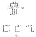
- Partitions can now be inserted into these slot-shaped receptacles 5 and 5 ', which in the exemplary embodiment according to FIG. 3 are formed as partition wall parts 6 formed on the underside of the insulating-material housing of the electrical-electronic components 3, while in the exemplary embodiment according to FIG. 4 electrical-electronic component 3' are shown, each of which is provided with a recess 7 into which separate individual partition wall pieces 6a can be inserted in a snap-locking manner if necessary.
- Some such separate partition wall pieces 6a, 6b, 6c are illustrated in FIG. 5.
- the dividing wall piece 6c While the dividing wall pieces 6a and 6b have upper latching lugs sprung via a slot, the dividing wall piece 6c has projecting latching knobs 8 arranged in its upper region on its wall surfaces.
- the receptacles 7 of the components 3 ' are each provided with correspondingly shaped counter-elements for the snap-locking receptacle in accordance with the configuration of the partition wall pieces.
- electrical-electronic components are particularly suitable for connecting terminals 3, 3', or terminal-like components with a corresponding insulating housing and soldering pins, as well as multipole connector strips, which are either integrally formed from the outset in a corresponding number of poles , or can be put together from individual elements to form blocks of the desired number of poles.
- insulating material housings from which solder pins protrude in a corresponding number and at a corresponding distance.
- the partitions 6, 6a, 6b, 6c which they are now molded onto the insulating material housing, or can be latched with them in a particularly expedient embodiment, bring about an extraordinary increase in creepage and clearance between the soldering pins concerned, since there is now a way to calculate them Partitions leads around, is to be used. It goes without saying that the separate individual partition wall pieces also consist of an insulating material.
Landscapes
- Engineering & Computer Science (AREA)
- Microelectronics & Electronic Packaging (AREA)
- Manufacturing & Machinery (AREA)
- Diaphragms For Electromechanical Transducers (AREA)
- Coupling Device And Connection With Printed Circuit (AREA)
- Superconductors And Manufacturing Methods Therefor (AREA)
- Techniques For Improving Reliability Of Storages (AREA)
- Oscillators With Electromechanical Resonators (AREA)
- Production Of Multi-Layered Print Wiring Board (AREA)
- Connector Housings Or Holding Contact Members (AREA)
- Multi-Conductor Connections (AREA)
- Combinations Of Printed Boards (AREA)
Description
- Die vorliegende Erfindung betrifft eine Leiterplattenanordnung, bestehend aus einer Leiterplatte mit einem vorgegebenen Raster von Aufnahmen und aus darauf angeordneten elektrisch-elektronischen, mit einem Isolierstoffgehäuse versehenen Bauteilen mit Lötanschlüssen.
- Leiterplatten sind üblicherweise mit in einem vorbestimmten Raster versehenen Aufnahmen in Form von Löchern versehen, in die darauf anzuordnende elektrisch-elektronische Bauteile mit den Stiften ihres Lötanschlusses entsprechend der jeweiligen Schaltungsanordnung eingesteckt und dann verlötet werden. Betroffen sind hier dabei derartige elektrische- elektronische Bauteile, die mit einem Isolierstoffgehäuse versehen sind, aus dem die Stifte der Lötanschlüsse vorstehen, also beispielsweise Anschlußklemmen für gedruckte Schaltungen (DE-AS 27 36 620), oder aber blokkartig zusammensetzbare oder von vornherein in vorbestimmter Polzahl einstückige Steckverbinderleisten (DE-AS 12 68 707, DE-OS 25 00 141
- Das bekannte und gängige Rastermaß bei den bekannten Leiterplatten ist nun so ausgelegt, daß der hieraus resultierende relativ geringe Abstand zwischen den Stiften der Lötanschlüsse bei einer Anreihung derartiger Anschlußklemmen oder bei einer Vielzahl von Stiften einer langen Steckverbinderleiste bei höheren Anforderungen an die Größe der Kriechstrecke problematisch wird. Es ist dabei darn zu denken, daß man zwar auf der Unterseite der Leiterplatten, dort wo die durchgesteckten Lötstifte verlötet werden, das Kriechstrekken-Problem mit einem Isolier-Schutzlack lösen kann, daß aber auf der Oberseite der Lieterplatte, dort, wo die Isolierstoffgehäuse der Bauteile auf der Oberfläche der Leiterplatte sitzen, doch immer ein kleiner, wenn auch kaum sichtbarer Spalt zwischen der Unterseite der Isolierstoffgehäuse der Bauteile und der Oberfläche der Leiterplatte verbleibt und dieser Spalt als Kriech- und Luftstrecke zu berücksichtigen ist.
- Problematisch wird das Kriech- und Luftstrekken-Problem insbesondere dann, wenn herkömmliche Leiterplatten mit dem üblichen Rastermaß bei sogenannten Eigenschutzanlagen Einsatz finden sollen, bei denen mit einer Anordnung beispielsweise in einem hochentzündlichen Gemisch gerechnet werden muß.
- Es könnte nun daran gedacht werden, für diese Einsatzzwecke spezielle Leiterplattenausgestaltungen mit entsprechend deutlich vergrößertem Rastermaß bei den Aufnahmen und entsprechend angepaßte aufzunehmende Bauteil mit entsprechend großem Lötstiftabstand vorzusehen, was jedoch eine spezielle, äußerst umzweckmäßige Fertigung und Lagerhaltung erfordern würde.
- Der vorliegenden Erfindung liegt von daher die Aufgabe zugrunde, eine Leiterplattenanordnung der gattungsgemäßen Art zu schaffen, die unter Verwendung der handelsüblichen Leiterplatten es ermöglicht, im Bedarfsfall in einfacher Weise Kriech- und Luftstreckenvergrößerungen zu erreichen.
- Die erindungsgemäße Lösung besteht darin, daß in der Leiterplatte in Anordnungsrichtung der Lötanschlüsse jeweils zwischen den Aufnahmen oder zwischen vorgegebenen Aufnahmegruppen Aussparungen vorgesehen sind und ferner darin eingesteckte Trennwandstücke aus Isolierstoff vorgesehen sind, die mit den Isolierstoffgehäusen der Bauteil verbunden sind.
- Dank der in die Aussparungen der Leiterplatte einzusetzenden Trennwandstücke läßt sich nunmehr auf sehr einfache Weise im Bedarfsfall die auf der Oberfläche der Leiterplatte zu berücksichtigende Kriech- und Luftstrecke zwischen zwei Lötstiften außerordentlich vergrößern. Der Berechnung ist nämlich nunmehr der Weg zugrundezulegen, der zwischen zwei vorgegebenen Lötstiften um diese Trennwandstücke herumführt. Es kann dabei daran gedacht werden, Bauteile, beispielsweise Anschlußklemmen oder Steckverbinderleisten vorzusehen, bei denen die Trennwandstücke von vornherein einstückig an entsprechender Stelle an deren Isolierstoffgehäuse angeformt sind. Noch zweckmäßiger ist jedoch eine Ausgestaltung, bei der in die Isolierstoffgehäuse lediglich Aussparungen eingeformt sind, in die gesonderte einzelne Trennwandstücke mit entsprechender Ausgestaltung rasten oderschnappend-verriegelnd eingesetzt werden können. Im letzteren Fall können die Bauteile mit ihren Isolierstoffgehäusen völlig einheitlich für Einsatzfälle ohne Kriechstrekken-Vergrößerung sowie auch für den Einsatzbereich mit Kriechstrecken-Vergrößerung eingesetzt werden, wobei im letzteren Fall dann lediglich an den erforderlichen Stellen die Trennwandstücke eingerastet werden.
- Gemäß einer weiteren zweckmäßigen Ausgestaltung ist vorgesehen, die im Randbereich der Leiterplatte vorgesehenen Aussparungen für die Trennwandstücke zum Rand hin offen auszubilden. Dies führt zur Montageerleichterung bei der Anbringung der Trennwandstücke.
- Ausführungsbeispiele von Leiterplattenanordnungen gemäß der Erfindung werden nachstehend unter Bezugnahme auf die Zeichnung näher beschrieben.
- Es zeigen
- Figur 1 eine schematisierte Teildraufsicht auf eine Leiterplatte einer derartigen Leiterplattenanordnung,
- Figur 2 eine schematisierte Teildraufsicht auf eine weitere derartige Leiterplatte,
- Figur 3 eine auf einer Leiterplatte angeordnete Anreihung von elektrisch-elektronischen Bauteilen einer derartigen Anordnung,
- Figur 4 eine weitere Ausführungsform derartiger Bauteile,
- Figur 5 EinzelansichtverschiedenerTrennwandstücke für eine derartige Leiterplattenanordnung.
- Die Leiterplattenanordnung beinhaltet eine Leiterplatte, wie die in zwei Ausführungsformen mit den Leiterplatten 1 und 1' in den Figuren 1 und 2 dargestellt ist. Die Leiterplatte 1 hat die üblichen Löcher 2 als Aufnahmen für die Lötanschlüsse der aufzubringenden Bauteile, wobei sich diese Aufnahmen 2 voneinander in einem Abstand entsprechend dem handelsüblichen Rastermaß bei derartigen Leiterplatten befinden. Aus diesem Rastermaß resultieren bei einer Anreihung von aufzubringenden Bauelementen dann auch die Abstände, die die Lötstifte voneinander haben, wie dies beispielsweise in Figure 3 für die dort als elektrisch-elektronische Bauteil vorgesehenen Anschlußklemmen 3 gezeigt ist, deren Lötstifte 4 einen entsprechenden Abstand voneinander haben. In Figur 3 ist dabei auch illustriert, daß sich nach Aufsetzen der Bauteile 3 auf die Leiterplatte 1 zwischen der Unterseite der Isolierstoffgehäuse der Bauteile 3, aus der die Lötstifte 4 vorstehen, und der Oberfläche der Leiterplatte 1 ein Luftspalt bildet, der in der Praxis häufig mit dem Auge kaum wahrnehmbar ist, der aber bei der Berechnung der Kriech- und Luftstrecken durchaus berücksichtigt werden muß.
- Es ist nun vorgesehen, in den Leiterplatten 1, 1' in Anordnungsrichtung der Lötanschlüsse der Bauteile zwischen den Aufnahmen 2, und zwar beispielsweise (Figur 1) zwischen jeder der Aufnahmen 2, schlitzförmige Aussparungen 5 vorzusehen. Bei der Ausführungsform nach Figur 2 sind in der Leiterplatte 1' jeweils zwischen einer Gruppe von zwei Aufnahmen 2 Schlitze vorgesehen, wobei im Ausführungsbeispiel nach Figur 2 im dort dargestellten Randbereich der Leiterplatte 1' schlitzförmige Aufnahmen 5' vorgesehen, die zum Rand hin offen sind.
- In diese schlitzförmigen Aufnahmen 5 bzw. 5' können nun Trennwandstücke eingesteckt werden, die im Ausführungsbeispiel nach Figur 3 als an die Isolierstoffgehäuse der elektrisch-elektronischen Bauteile 3 unterseitig angeformte Trennwandstücke 6 ausgebildet sind, während im Ausführungsbeispiel nach Figur 4 elektrisch-elektronische Bauelement 3' gezeigt sind, die jeweils mit einer Aussparung 7 versehen sind, in die gesonderte einzelne Trennwandstücke 6a im Bedarfsfall schnappend-verriegelnd eingesetzt werden können. Einige derartige gesonderte Trennwandstücke 6a, 6b, 6c sind in Figur 5 illustriert. Während die Trennwandstücke 6a und 6b über einen Schlitz abgefederte obere Rastnasen haben, weist das Trennwandstück 6c in seinem oberen Bereich auf seinen Wandflächen angeordnete vorstehende Rastnoppen 8 auf. Die Aufnahmen 7 der Bauteile 3' sind jeweils entsprechend der Ausgestaltung der Trennwandstücke mit entsprechend geformten Gegenelementen für die schnappend-verriegelnde Aufnahme versehen.
- Also auf der Leiterplatte 1, 1' anzubringende elektrisch-elektronische Bauteile kommen insbesondere Anschlußklemmen 3,3' in Betracht, oder aber anschlußklemmenartig ausgebildete Bauteile mit einem entsprechenden Isolierstoffgehäuse und Lötstiften, sowie ferner mehrpolige Steckverbinderleisten, die entweder von vornherein einstückig in entsprechender Polzahl ausgebildet sind, oder aus einzelnen Elementen zu Blocks der gewünschten Polzahl zusammengesteckt werden können. Auch hier sind dann wieder Isolierstoffgehäuse vorhanden, aus denen in entsprechender Anzahl und in entsprechendem Abstand Lötstifte vorstehen.
- Die Trennwände 6, 6a, 6b, 6c, seine sie nun an die Isolierstoffgehäuse angeformt, oder aber in besonders zweckmäßiger Ausgestaltung mit diesen verrastbar, bewirken eine außerordentliche Kriech- und Luftstreckenvergrößerung zwischen betroffenen Lötstiften, da für deren Berechnung jetzt ein Weg, der um die Trennwandstücke herumführt, zugrundezulegen ist. Es versteht sich dabei, daß auch die gesonderten einzelnen Trennwandstücke aus einem Isolierstoff bestehen.
Claims (6)
Priority Applications (1)
| Application Number | Priority Date | Filing Date | Title |
|---|---|---|---|
| AT85105125T ATE59128T1 (de) | 1984-06-27 | 1985-04-26 | Leiterplattenanordnung. |
Applications Claiming Priority (2)
| Application Number | Priority Date | Filing Date | Title |
|---|---|---|---|
| DE3423648 | 1984-06-27 | ||
| DE3423648A DE3423648C1 (de) | 1984-06-27 | 1984-06-27 | Leiterplattenanordnung |
Publications (3)
| Publication Number | Publication Date |
|---|---|
| EP0166110A2 EP0166110A2 (de) | 1986-01-02 |
| EP0166110A3 EP0166110A3 (en) | 1988-09-07 |
| EP0166110B1 true EP0166110B1 (de) | 1990-12-12 |
Family
ID=6239256
Family Applications (1)
| Application Number | Title | Priority Date | Filing Date |
|---|---|---|---|
| EP85105125A Expired - Lifetime EP0166110B1 (de) | 1984-06-27 | 1985-04-26 | Leiterplattenanordnung |
Country Status (3)
| Country | Link |
|---|---|
| EP (1) | EP0166110B1 (de) |
| AT (1) | ATE59128T1 (de) |
| DE (2) | DE3423648C1 (de) |
Families Citing this family (2)
| Publication number | Priority date | Publication date | Assignee | Title |
|---|---|---|---|---|
| US6747862B1 (en) * | 2000-07-17 | 2004-06-08 | Alcatel | System and method for providing high voltage withstand capability between pins of a high-density compliant pin connector |
| DE102019129375A1 (de) | 2019-10-30 | 2021-05-06 | Harting Electric Gmbh & Co. Kg | Leiterkarte mit Isoliereinheit |
Family Cites Families (4)
| Publication number | Priority date | Publication date | Assignee | Title |
|---|---|---|---|---|
| BE653673A (de) * | 1963-09-27 | |||
| DE1268707B (de) * | 1966-06-11 | |||
| FR1521897A (fr) * | 1966-06-11 | 1968-04-19 | Barrette de connexion électrique multipolaire | |
| DE2500141A1 (de) * | 1974-01-23 | 1975-07-24 | Gen Signal Corp | Elektrisches anschlusstueck mit variabler laenge |
-
1984
- 1984-06-27 DE DE3423648A patent/DE3423648C1/de not_active Expired
-
1985
- 1985-04-26 DE DE8585105125T patent/DE3580869D1/de not_active Expired - Fee Related
- 1985-04-26 AT AT85105125T patent/ATE59128T1/de not_active IP Right Cessation
- 1985-04-26 EP EP85105125A patent/EP0166110B1/de not_active Expired - Lifetime
Also Published As
| Publication number | Publication date |
|---|---|
| EP0166110A3 (en) | 1988-09-07 |
| EP0166110A2 (de) | 1986-01-02 |
| ATE59128T1 (de) | 1990-12-15 |
| DE3423648C1 (de) | 1985-10-17 |
| DE3580869D1 (de) | 1991-01-24 |
Similar Documents
| Publication | Publication Date | Title |
|---|---|---|
| EP0456987B1 (de) | Anschlussleiste für die Fernmeldetechnik | |
| DE69117703T2 (de) | Steckverbindersystem von hoher Dichte | |
| DE3883805T2 (de) | An der Oberfläche montierbarer elektrischer Stecker. | |
| DE69400551T2 (de) | Verbinderanordnung für gedruckte Leiterplatte | |
| DE69309438T2 (de) | System und steckverbinder für die elektrische zwischenverbindung von leiterplatten | |
| DE3137429A1 (de) | Vorrichtung zur herstellung eines loet,- schraub- undabisolierfreien einfach- oder mehrfachkontaktes an einem anschlusselement | |
| DE3447347A1 (de) | Gehaeuse fuer elektronische vorrichtungen | |
| DE102019102111A1 (de) | Elektrischer Verbinder, insbesondere abgeschirmter Vertikalsockel-Verbinder | |
| DE2646616C3 (de) | Anreihbares Einbauteil | |
| DE3213884A1 (de) | Anschlussvorrichtung fuer ein plattenfoermiges elektrisches geraet | |
| DE3446622A1 (de) | Steckereinsatz fuer stecker mit hoher steckhaeufigkeit | |
| DE2723201A1 (de) | Elektrisches bauelement mit winkeladapter und verfahren zu dessen herstellung | |
| DE2812332B2 (de) | Vielfachsteckverbindung für Karten mit gedruckter Schaltung | |
| EP0658955B1 (de) | Planarfilter für einen vielpoligen Steckverbinder | |
| DE3423648C1 (de) | Leiterplattenanordnung | |
| DE69206325T2 (de) | Mikrowellenverbinderanordnung mit einfachem Anschluss an Mikrowellenschaltelemente. | |
| EP0555653A1 (de) | Schalterstecker | |
| EP0171808B1 (de) | Relaissockel eines elektromagnetischen Relais | |
| DE8426609U1 (de) | Hörgerät | |
| DE3816853C1 (en) | Cover for the connecting pins of connector strips | |
| DE2643088A1 (de) | Verteileranordnung fuer fernmeldevermittlungsanlagen | |
| EP0595304B1 (de) | Schirmeinrichtung für rechteckige Kabelstecker | |
| DE8422793U1 (de) | Vorrichtung zur Aufnahme wenigstens einer Baugruppe | |
| DE1258934B (de) | Kontaktloses Steuer- und Regelement | |
| DE2543513C3 (de) | Steckverbindung |
Legal Events
| Date | Code | Title | Description |
|---|---|---|---|
| PUAI | Public reference made under article 153(3) epc to a published international application that has entered the european phase |
Free format text: ORIGINAL CODE: 0009012 |
|
| AK | Designated contracting states |
Designated state(s): AT CH DE FR GB IT LI NL SE |
|
| PUAL | Search report despatched |
Free format text: ORIGINAL CODE: 0009013 |
|
| AK | Designated contracting states |
Kind code of ref document: A3 Designated state(s): AT CH DE FR GB IT LI NL SE |
|
| 17P | Request for examination filed |
Effective date: 19880920 |
|
| 17Q | First examination report despatched |
Effective date: 19900426 |
|
| ITF | It: translation for a ep patent filed | ||
| GRAA | (expected) grant |
Free format text: ORIGINAL CODE: 0009210 |
|
| AK | Designated contracting states |
Kind code of ref document: B1 Designated state(s): AT CH DE FR GB IT LI NL SE |
|
| REF | Corresponds to: |
Ref document number: 59128 Country of ref document: AT Date of ref document: 19901215 Kind code of ref document: T |
|
| GBT | Gb: translation of ep patent filed (gb section 77(6)(a)/1977) | ||
| REF | Corresponds to: |
Ref document number: 3580869 Country of ref document: DE Date of ref document: 19910124 |
|
| ET | Fr: translation filed | ||
| PLBE | No opposition filed within time limit |
Free format text: ORIGINAL CODE: 0009261 |
|
| STAA | Information on the status of an ep patent application or granted ep patent |
Free format text: STATUS: NO OPPOSITION FILED WITHIN TIME LIMIT |
|
| 26N | No opposition filed | ||
| REG | Reference to a national code |
Ref country code: FR Ref legal event code: CD |
|
| PGFP | Annual fee paid to national office [announced via postgrant information from national office to epo] |
Ref country code: FR Payment date: 19940125 Year of fee payment: 10 |
|
| PGFP | Annual fee paid to national office [announced via postgrant information from national office to epo] |
Ref country code: AT Payment date: 19940414 Year of fee payment: 10 |
|
| PGFP | Annual fee paid to national office [announced via postgrant information from national office to epo] |
Ref country code: SE Payment date: 19940415 Year of fee payment: 10 |
|
| PGFP | Annual fee paid to national office [announced via postgrant information from national office to epo] |
Ref country code: GB Payment date: 19940418 Year of fee payment: 10 |
|
| PGFP | Annual fee paid to national office [announced via postgrant information from national office to epo] |
Ref country code: DE Payment date: 19940426 Year of fee payment: 10 |
|
| PGFP | Annual fee paid to national office [announced via postgrant information from national office to epo] |
Ref country code: NL Payment date: 19940430 Year of fee payment: 10 |
|
| EAL | Se: european patent in force in sweden |
Ref document number: 85105125.0 |
|
| PG25 | Lapsed in a contracting state [announced via postgrant information from national office to epo] |
Ref country code: GB Effective date: 19950426 Ref country code: AT Effective date: 19950426 |
|
| PG25 | Lapsed in a contracting state [announced via postgrant information from national office to epo] |
Ref country code: SE Effective date: 19950427 |
|
| PG25 | Lapsed in a contracting state [announced via postgrant information from national office to epo] |
Ref country code: NL Effective date: 19951101 |
|
| GBPC | Gb: european patent ceased through non-payment of renewal fee |
Effective date: 19950426 |
|
| PG25 | Lapsed in a contracting state [announced via postgrant information from national office to epo] |
Ref country code: FR Effective date: 19951229 |
|
| NLV4 | Nl: lapsed or anulled due to non-payment of the annual fee |
Effective date: 19951101 |
|
| PG25 | Lapsed in a contracting state [announced via postgrant information from national office to epo] |
Ref country code: DE Effective date: 19960103 |
|
| EUG | Se: european patent has lapsed |
Ref document number: 85105125.0 |
|
| REG | Reference to a national code |
Ref country code: FR Ref legal event code: ST |
|
| PGFP | Annual fee paid to national office [announced via postgrant information from national office to epo] |
Ref country code: CH Payment date: 19960604 Year of fee payment: 12 |
|
| PG25 | Lapsed in a contracting state [announced via postgrant information from national office to epo] |
Ref country code: LI Free format text: LAPSE BECAUSE OF NON-PAYMENT OF DUE FEES Effective date: 19970430 Ref country code: CH Free format text: LAPSE BECAUSE OF NON-PAYMENT OF DUE FEES Effective date: 19970430 |
|
| REG | Reference to a national code |
Ref country code: CH Ref legal event code: PL |