EP0164675A2 - Abhebe-Verfahren - Google Patents
Abhebe-Verfahren Download PDFInfo
- Publication number
- EP0164675A2 EP0164675A2 EP85106842A EP85106842A EP0164675A2 EP 0164675 A2 EP0164675 A2 EP 0164675A2 EP 85106842 A EP85106842 A EP 85106842A EP 85106842 A EP85106842 A EP 85106842A EP 0164675 A2 EP0164675 A2 EP 0164675A2
- Authority
- EP
- European Patent Office
- Prior art keywords
- layer
- substrate
- lift
- ambient
- polymer
- Prior art date
- Legal status (The legal status is an assumption and is not a legal conclusion. Google has not performed a legal analysis and makes no representation as to the accuracy of the status listed.)
- Withdrawn
Links
Images

Classifications
-
- H—ELECTRICITY
- H01—ELECTRIC ELEMENTS
- H01L—SEMICONDUCTOR DEVICES NOT COVERED BY CLASS H10
- H01L21/00—Processes or apparatus adapted for the manufacture or treatment of semiconductor or solid state devices or of parts thereof
- H01L21/70—Manufacture or treatment of devices consisting of a plurality of solid state components formed in or on a common substrate or of parts thereof; Manufacture of integrated circuit devices or of parts thereof
- H01L21/71—Manufacture of specific parts of devices defined in group H01L21/70
- H01L21/768—Applying interconnections to be used for carrying current between separate components within a device comprising conductors and dielectrics
- H01L21/76838—Applying interconnections to be used for carrying current between separate components within a device comprising conductors and dielectrics characterised by the formation and the after-treatment of the conductors
- H01L21/76877—Filling of holes, grooves or trenches, e.g. vias, with conductive material
- H01L21/7688—Filling of holes, grooves or trenches, e.g. vias, with conductive material by deposition over sacrificial masking layer, e.g. lift-off
-
- G—PHYSICS
- G03—PHOTOGRAPHY; CINEMATOGRAPHY; ANALOGOUS TECHNIQUES USING WAVES OTHER THAN OPTICAL WAVES; ELECTROGRAPHY; HOLOGRAPHY
- G03F—PHOTOMECHANICAL PRODUCTION OF TEXTURED OR PATTERNED SURFACES, e.g. FOR PRINTING, FOR PROCESSING OF SEMICONDUCTOR DEVICES; MATERIALS THEREFOR; ORIGINALS THEREFOR; APPARATUS SPECIALLY ADAPTED THEREFOR
- G03F7/00—Photomechanical, e.g. photolithographic, production of textured or patterned surfaces, e.g. printing surfaces; Materials therefor, e.g. comprising photoresists; Apparatus specially adapted therefor
- G03F7/004—Photosensitive materials
- G03F7/039—Macromolecular compounds which are photodegradable, e.g. positive electron resists
-
- H—ELECTRICITY
- H01—ELECTRIC ELEMENTS
- H01L—SEMICONDUCTOR DEVICES NOT COVERED BY CLASS H10
- H01L21/00—Processes or apparatus adapted for the manufacture or treatment of semiconductor or solid state devices or of parts thereof
- H01L21/02—Manufacture or treatment of semiconductor devices or of parts thereof
- H01L21/027—Making masks on semiconductor bodies for further photolithographic processing not provided for in group H01L21/18 or H01L21/34
- H01L21/0271—Making masks on semiconductor bodies for further photolithographic processing not provided for in group H01L21/18 or H01L21/34 comprising organic layers
- H01L21/0272—Making masks on semiconductor bodies for further photolithographic processing not provided for in group H01L21/18 or H01L21/34 comprising organic layers for lift-off processes
-
- H—ELECTRICITY
- H05—ELECTRIC TECHNIQUES NOT OTHERWISE PROVIDED FOR
- H05K—PRINTED CIRCUITS; CASINGS OR CONSTRUCTIONAL DETAILS OF ELECTRIC APPARATUS; MANUFACTURE OF ASSEMBLAGES OF ELECTRICAL COMPONENTS
- H05K3/00—Apparatus or processes for manufacturing printed circuits
- H05K3/02—Apparatus or processes for manufacturing printed circuits in which the conductive material is applied to the surface of the insulating support and is thereafter removed from such areas of the surface which are not intended for current conducting or shielding
- H05K3/04—Apparatus or processes for manufacturing printed circuits in which the conductive material is applied to the surface of the insulating support and is thereafter removed from such areas of the surface which are not intended for current conducting or shielding the conductive material being removed mechanically, e.g. by punching
- H05K3/046—Apparatus or processes for manufacturing printed circuits in which the conductive material is applied to the surface of the insulating support and is thereafter removed from such areas of the surface which are not intended for current conducting or shielding the conductive material being removed mechanically, e.g. by punching by selective transfer or selective detachment of a conductive layer
- H05K3/048—Apparatus or processes for manufacturing printed circuits in which the conductive material is applied to the surface of the insulating support and is thereafter removed from such areas of the surface which are not intended for current conducting or shielding the conductive material being removed mechanically, e.g. by punching by selective transfer or selective detachment of a conductive layer using a lift-off resist pattern or a release layer pattern
-
- Y—GENERAL TAGGING OF NEW TECHNOLOGICAL DEVELOPMENTS; GENERAL TAGGING OF CROSS-SECTIONAL TECHNOLOGIES SPANNING OVER SEVERAL SECTIONS OF THE IPC; TECHNICAL SUBJECTS COVERED BY FORMER USPC CROSS-REFERENCE ART COLLECTIONS [XRACs] AND DIGESTS
- Y10—TECHNICAL SUBJECTS COVERED BY FORMER USPC
- Y10S—TECHNICAL SUBJECTS COVERED BY FORMER USPC CROSS-REFERENCE ART COLLECTIONS [XRACs] AND DIGESTS
- Y10S438/00—Semiconductor device manufacturing: process
- Y10S438/942—Masking
- Y10S438/948—Radiation resist
- Y10S438/951—Lift-off
Definitions
- This invention relates to a lift-off process for forming metal patterns on substrates.
- a typical process for forming metal patterns like an interconnection metallurgy system for integrated circuit devices, includes delineation of a desired metallurgy pattern by the resist-expose-develop sequence followed by sputter etching or RIE and metal deposition. Second metal level is similarly defined to form metal to metal contact with the underlying layer through via holes in an insulating layer between the two levels.
- Alternative methods commonly employed for multilevel metal processes in integrated circuits are termed "expendable mask method", “lift-off method” or “stencil method” as described in the following references:
- the preferred materials for the planar process claimed in U.S. Patent No. 3,985,597 are: polyimide for the base layer, polysulfone resins, such as those available from ICI (Imperial Chemical Industry) for the "lift-off” layer, glass resin polymer (for example, "glass resin” type 650 from Owens Illinois, Inc.), for the masking layer which is overcoated with a photoresist layer.
- polyimide for the base layer
- polysulfone resins such as those available from ICI (Imperial Chemical Industry) for the "lift-off” layer
- glass resin polymer for example, "glass resin” type 650 from Owens Illinois, Inc.
- this approach is designed to provide planar multilevel metal processes which are of crucial importance in large scale integrated circuit fabrication to eliminate the failure mechanisms originating from possible current crowding of metallurgical lines and electromigration, it is subject to limitations in the performance of the conventional polysulfone resin, as the lift-off layer.
- a protracted soak in a powerful solvent such as NMP at 80-85° is required to cause "lift-off" with this material.
- the fully cured polyimide base layer swells due to solvent permeation causing stress cracking of the silicon nitride film used as a built-in etch stop.
- the soak time necessary for lift-off is variable and is affected by the process conditions employed for metal deposition. For example, it is observed that a longer soak time is required when metallization is carried out by electron beam evaporation as compared to RF evaporation.
- the coatings are to be carried out under low controlled humidity but still occasional problems of film dewetting during spin application on various substrates, and cracking of contacting layers are observed upon curing at high temperature.
- the invention disclosed herein provides an improved lift-off process in the fabrication of metal structures through the use of - preferably thermally - depolymerizable polymers for the lift-off layer.
- a thermally depolymerizable polymer is removed efficiently by first subjecting the post-metallized structure to short-thermal treatment at the depolymerization temperature of the lift-off polymeric system, and subsequent short solvent soak.
- the inventive process replaces the conventional polysulfone lift-off layers with depolymerizable polymer coatings. This obviates protracted exposure to powerful solvent such as N-methylpyrrolidone.
- the lift-off coatings used in the inventive process are free from humidity related problems, have superior adhesion to most organic or inorganic contacting films, and can be cast from solvents which can be removed at relatively low temperature.
- the inventive process in a preferred embodiment involves forming on a substrate a base layer of a thermosetting resin such as polyimide followed sequentially by an oxygen RIE barrier layer, the depolymerizable polymer layer, an oxygen RIE barrier layer and finally a resist layer.
- a desired metallurgy pattern is defined by the conventional lithographic process, replicated into the underlying layers by RIE followed by the metallization step such that the metallization temperature is at least 30-50° below the decomposition temperature of the lift-off polymer selected.
- the release of the lift-off is then accomplished by heating the structure for 2-10 minutes followed by solvent soak which requires relatively short times since the prior thermal treatment causes enough disruption, adhesion failure and porosity in the film structure to allow effective solvent permeation and accelerated di -olu- tion of the oligomeric species generated.
- inventive process to prcvide crack-free via structures prepared with organic insulators such as polyimide, polyphenylenes, poly- quinoxalines, etc. along with other high temperature polymers, and inorganic barrier layers such as silicon nitride or silicon oxide. This is so because the inventive process obviates swelling of the underlying organic insulator film. In the known methods this swelling causes cracking of the overlying barrier film such as silicon nitride or silicon oxide.
- the inventive process is especially suitable for forming reliable multilevel-metal-structures.
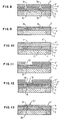
- a process for forming metallurgical pattern on a substrate is illustrated in Figures 1 to 13 for various states in the fabrication of multilevel metal structure utilizing concepts/materials/processes described in this invention.
- These improved materials for the lift-off layer are characterized by high glass transition temperature (Tg > 100°C) and may be employed as replacement for polysulfones in the conventional process using silicon nitride or silicon oxide as barrier layers or in a modified packaging scheme using plasma-polymerized organosilicons as oxygen RIE barriers and a second dielectric as disclosed in the co-pending application Serial No. 565,562 filed, December 27, 1983, for 'Multilevel Metal Structures and Process Using Plasma Polymerized Organosilicon Films" (PO 9-83-005).
- Tg > 100°C high glass transition temperature
- Polymers suitable for use in the practice of this invention include the following:
- the preferred materials of this invention have medium to high molecular weights with relatively narrow molecular weight distribution to assure uniformity of functional performance.
- preferred molecular weight range is from 60,000 to 100,000.
- poly-(a-methylstyrene) from 20,000 to medium MW of about 200,000 and high MW of about 500,000 and for poly (MMA-MAA) with 65:35 MMA to MAA ratio, the preferred molecular weight range is 40,000 to about 80,000.
- "atactic" configuration is particularly preferred for the purpose of this invention.
- films derived from higher molecular weight materials have superior mechanical integrity and adhesion with contacting films.
- a multilevel metal process using the lift-off materials of the present invention consists of the following generalized sequence of steps as illustrated in Figures I to 13, of which specific descriptions follow thereafter.
- a substrate typically a semiconductor monocrystalline silicon or a ceramic or glass with metal lines, (not shown) is provided with an overlying layer 2 of a dielectric as for example Si 3 N 4 , SiO 2 , SiOx or Ta 2 0 5 .
- the substrate 1 for purpose of illustration, can be an integrated circuit device having active and passive devices fabricated therein (not shown) which are suitably isolated from each other.
- the dielectric layer 2 is provided with contact openings (not shown here) for making electrical contact with devices underneath.
- the substrate could also be glass-ceramic or alumina ceramic with metallurgy for appropriate integrated circuit devices with associated circuitry.
- a layer 3 of an insulator organic resin is deposited over layer 2.
- the material for this layer can be the polyimide Pyralin (RC-5878) manufactured by E. I. duPont deNemours, which is applied in thickness of 1-5 ⁇ m.
- the preferred thickness is 1-2 ⁇ m while for packaging 4-5 ⁇ m thick film can be employed.
- layer 4 which comprises an organic polymer depolymerizable under the influence of heat.
- Typical materials for this layer are polymethylmethacrylate, poly (methacrylic acid, poly-a-methylstyrene, methacrylic anhydride methylmethacrylate) terpolymer prepared by heating a methylmethacrylate-methacrylic acid copolymer (60:40) at 220-240°C for a period of 20-40 minutes.
- poly(pentene-l-sulfone) and polyalkylaryl ketones are also used.
- Typical thickness for the layer 4 is 0.3-1 ⁇ m for integrated circuit device, and 1-3 ⁇ m for packaging.
- thermally depolymerizable polymers for facilitating lift-off represents a major departure from the previous art.
- the deposited layer 5, as shown in Fig. 3, can be any material resistant to reactive ion etching, where the material of this layer can be plasma deposited organosilicon, like divinyl tetramethyl disiloxane or hexamethyldisilazane (1200-2000 A) as discussed in copending application Serial No. 565,562 for "Multilevel Metal Structures and Process Using Plasma Polymerized Organosilicon Films" filed December 27, 1983, or Si X N Y H Z .
- inorganic materials such as SiO X , SiO 2 , Al 2 O 3 , and the like, can also be deposited and employed.
- plasma deposited organosilicon layer it is preferably annealed at about 250°C for 10 minutes subsequent to deposition.
- a layer 6 of a positive photoresist as for example, the azoplate novolak type resist, AZ 1350 J, is then deposited on layer 5 according to well established technology.
- the imaged pattern after development is transferred as vias or access openings 50 into layers 5, 4 and 3 according to the methodology described in U.S. Patent 4,367,119 and said copending application Serial No. 565,562.
- the metallization also results in metal deposition on layer 2 through the openings 50.
- the thickness of layer is preferably approximately equal to that of 3.
- Fig. 5 Shown in Fig. 5 is the structure obtained upon removal of all the layers above patterned layer 3 which is accomplished as given in the following.
- the substrate is heated at 290-300°C under nitrogen for 10 minutes and immediately transferred to a diglyme or diglyme-NMP bath at 60° equipped with Macronatics Jet Etcher (manufactured by Macronatics Inc. CA).
- the lift-off is invariably complete in 1-10 minutes.
- the substrate is rinsed in diglyme and finally in deionized water.
- the resultant metal patterns or segments 7A surrounded by patterned layer 3, e.g. the aforesaid (Polyimide 5878) are essentially planar.
- post metallization sintering is carried out above 300°C in a reducing atmosphere.
- the small gaps or spaces 8 are filled with the polyimide used for layer 3' or any other suitable resin plastic when the second sequence of steps is used to form the next level of metallurgy. Again it is preferred to use duPont polyimide RC-5878 in two coats to achieve gap filling and higher planarization.
- the layers 4', 5' in Fig. 6 correspond to layers 4 and 5 in Fig. 2.
- a layer of photoresist 6' is then deposited on layer 5' and patterned suitably to furnish the via hole pattern 10 (Fig. 7) after sequentially developing the resist layer 6'; reactive ion etching of layer 5' with CF 4 ambient laver; 4' with O 2 , ambient; layer 9 with CF 4 or a mixture of O 2 +CF 4 ; and finally with, 0 2 ambient again to make contact with 7A.
- a few seconds of optional sputter clean is recommended for removal of any trace residues on metal pattern or segments 7A.
- a metal layer 7' is then again blanket deposited leading to formation of the studs 7B in contact with metallurgy 7A to give the structure represented by Fig. 8.
- Lift-off is again carried out by first heating at the depolymerization temperature of the lift-off terpolymer that constitutes layer 4' i.e. heating at 290-300° in nitrogen 5-15 minutes followed by quick transfer to a diglyme or diglyme-NMP (1:1) both equipped with Macronatics Jet Etcher. The lift-off is accomplished in 1-10 minutes. Again the metallurgy is annealed as before. The resultant structure is shown in Fig. 9.
Landscapes
- Engineering & Computer Science (AREA)
- Physics & Mathematics (AREA)
- Manufacturing & Machinery (AREA)
- Microelectronics & Electronic Packaging (AREA)
- General Physics & Mathematics (AREA)
- Computer Hardware Design (AREA)
- Condensed Matter Physics & Semiconductors (AREA)
- Power Engineering (AREA)
- Spectroscopy & Molecular Physics (AREA)
- Internal Circuitry In Semiconductor Integrated Circuit Devices (AREA)
- Drying Of Semiconductors (AREA)
- Weting (AREA)
- Photosensitive Polymer And Photoresist Processing (AREA)
Applications Claiming Priority (2)
| Application Number | Priority Date | Filing Date | Title |
|---|---|---|---|
| US619516 | 1984-06-11 | ||
| US06/619,516 US4519872A (en) | 1984-06-11 | 1984-06-11 | Use of depolymerizable polymers in the fabrication of lift-off structure for multilevel metal processes |
Publications (2)
| Publication Number | Publication Date |
|---|---|
| EP0164675A2 true EP0164675A2 (de) | 1985-12-18 |
| EP0164675A3 EP0164675A3 (de) | 1987-06-16 |
Family
ID=24482225
Family Applications (1)
| Application Number | Title | Priority Date | Filing Date |
|---|---|---|---|
| EP85106842A Withdrawn EP0164675A3 (de) | 1984-06-11 | 1985-06-03 | Abhebe-Verfahren |
Country Status (5)
| Country | Link |
|---|---|
| US (1) | US4519872A (de) |
| EP (1) | EP0164675A3 (de) |
| JP (1) | JPH0646629B2 (de) |
| BR (1) | BR8502757A (de) |
| CA (1) | CA1212890A (de) |
Families Citing this family (47)
| Publication number | Priority date | Publication date | Assignee | Title |
|---|---|---|---|---|
| JPS613339A (ja) * | 1984-06-18 | 1986-01-09 | Hitachi Ltd | 高密度情報記録円板複製用スタンパおよびその製造方法 |
| US4631806A (en) * | 1985-05-22 | 1986-12-30 | Gte Laboratories Incorporated | Method of producing integrated circuit structures |
| FR2588418B1 (fr) * | 1985-10-03 | 1988-07-29 | Bull Sa | Procede de formation d'un reseau metallique multicouche d'interconnexion des composants d'un circuit integre de haute densite et circuit integre en resultant |
| FR2588417B1 (fr) * | 1985-10-03 | 1988-07-29 | Bull Sa | Procede de formation d'un reseau metallique multicouche d'interconnexion des composants d'un circuit integre de haute densite et circuit integre en resultant |
| WO1987005441A1 (en) * | 1986-03-05 | 1987-09-11 | Sumitomo Electric Industries, Ltd. | Semiconductor device and a method of producing the same |
| US4886573A (en) * | 1986-08-27 | 1989-12-12 | Hitachi, Ltd. | Process for forming wiring on substrate |
| EP0261846B1 (de) * | 1986-09-17 | 1992-12-02 | Fujitsu Limited | Verfahren zur Ausbildung einer Kupfer enthaltenden Metallisierungsschicht auf der Oberfläche eines Halbleiterbauelementes |
| JPS63104425A (ja) * | 1986-10-09 | 1988-05-09 | インタ−ナショナル・ビジネス・マシ−ンズ・コ−ポレ−ション | バイアの形成方法 |
| US5147741A (en) * | 1987-03-20 | 1992-09-15 | International Business Machines Corporation | Phenyl-endcapped depolymerizable polymer |
| US4835086A (en) * | 1988-02-12 | 1989-05-30 | Hoechst Celanese Corporation | Polysulfone barrier layer for bi-level photoresists |
| US4861425A (en) * | 1988-08-22 | 1989-08-29 | International Business Machines Corporation | Lift-off process for terminal metals |
| US5258264A (en) * | 1989-07-06 | 1993-11-02 | International Business Machines Corporation | Process of forming a dual overhang collimated lift-off stencil with subsequent metal deposition |
| US5024896A (en) * | 1989-07-06 | 1991-06-18 | International Business Machines Corporation | Collimated metal deposition |
| FR2650472A1 (fr) * | 1989-07-27 | 1991-02-01 | Bull Sa | Procede de depot d'une couche isolante sur une couche conductrice du reseau multicouche d'une carte de connexion de circuit integre de haute densite, et carte en resultant |
| US5112448A (en) * | 1989-11-28 | 1992-05-12 | The Boeing Company | Self-aligned process for fabrication of interconnect structures in semiconductor applications |
| US5130275A (en) * | 1990-07-02 | 1992-07-14 | Digital Equipment Corp. | Post fabrication processing of semiconductor chips |
| US5240878A (en) * | 1991-04-26 | 1993-08-31 | International Business Machines Corporation | Method for forming patterned films on a substrate |
| US5277749A (en) * | 1991-10-17 | 1994-01-11 | International Business Machines Corporation | Methods and apparatus for relieving stress and resisting stencil delamination when performing lift-off processes that utilize high stress metals and/or multiple evaporation steps |
| JPH05243223A (ja) * | 1992-02-28 | 1993-09-21 | Fujitsu Ltd | 集積回路装置の製造方法 |
| US5434451A (en) * | 1993-01-19 | 1995-07-18 | International Business Machines Corporation | Tungsten liner process for simultaneous formation of integral contact studs and interconnect lines |
| US5451295A (en) * | 1994-04-12 | 1995-09-19 | Micron Technology, Inc. | Process for removing film from a substrate |
| US5722162A (en) * | 1995-10-12 | 1998-03-03 | Fujitsu Limited | Fabrication procedure for a stable post |
| US5776805A (en) * | 1995-12-29 | 1998-07-07 | Lg Semicon Co., Ltd. | Method for manufacturing MESFET |
| TW505984B (en) | 1997-12-12 | 2002-10-11 | Applied Materials Inc | Method of etching patterned layers useful as masking during subsequent etching or for damascene structures |
| US6143476A (en) * | 1997-12-12 | 2000-11-07 | Applied Materials Inc | Method for high temperature etching of patterned layers using an organic mask stack |
| US6352918B1 (en) * | 1998-11-24 | 2002-03-05 | United Microelectronics Corp. | Method of forming inter-metal interconnection |
| US6413854B1 (en) | 1999-08-24 | 2002-07-02 | International Business Machines Corp. | Method to build multi level structure |
| DE19952018C1 (de) * | 1999-10-28 | 2001-08-23 | Martin Moeller | Verfahren zur Herstellung von im Nanometerbereich oberflächendekorierten Substraten |
| US6444402B1 (en) | 2000-03-21 | 2002-09-03 | International Business Machines Corporation | Method of making differently sized vias and lines on the same lithography level |
| US6383943B1 (en) | 2000-10-16 | 2002-05-07 | Taiwan Semiconductor Manufacturing Company | Process for improving copper fill integrity |
| US6495912B1 (en) * | 2001-09-17 | 2002-12-17 | Megic Corporation | Structure of ceramic package with integrated passive devices |
| US6913870B2 (en) * | 2002-05-10 | 2005-07-05 | International Business Machines Corporation | Fabrication process using a thin liftoff stencil formed by an image transfer process |
| US7129590B2 (en) * | 2003-05-14 | 2006-10-31 | Intel Corporation | Stencil and method for depositing material onto a substrate |
| DE102004059965A1 (de) * | 2004-12-13 | 2006-06-14 | Epcos Ag | Dünnschichtresonator und Verfahren zur Herstellung eines Vielschichtbauelements |
| KR100919636B1 (ko) * | 2005-06-30 | 2009-09-30 | 엘지디스플레이 주식회사 | 리프트 오프를 이용한 패턴 형성 방법과 이를 이용한액정표시장치용 어레이 기판의 제조방법 |
| US20080217730A1 (en) * | 2007-03-07 | 2008-09-11 | Toshiharu Furukawa | Methods of forming gas dielectric and related structure |
| US7579232B1 (en) * | 2008-07-11 | 2009-08-25 | Sandisk 3D Llc | Method of making a nonvolatile memory device including forming a pillar shaped semiconductor device and a shadow mask |
| JP5620669B2 (ja) * | 2009-10-26 | 2014-11-05 | 東芝機械株式会社 | レーザダイシング方法およびレーザダイシング装置 |
| JP5452247B2 (ja) * | 2010-01-21 | 2014-03-26 | 東芝機械株式会社 | レーザダイシング装置 |
| JP5981094B2 (ja) | 2010-06-24 | 2016-08-31 | 東芝機械株式会社 | ダイシング方法 |
| JP5140198B1 (ja) | 2011-07-27 | 2013-02-06 | 東芝機械株式会社 | レーザダイシング方法 |
| JP2014011358A (ja) | 2012-06-29 | 2014-01-20 | Toshiba Mach Co Ltd | レーザダイシング方法 |
| US8703611B1 (en) * | 2013-04-12 | 2014-04-22 | United Microelectronics Corp. | Method for manufacturing a semiconductor structure |
| KR102603867B1 (ko) * | 2016-08-01 | 2023-11-21 | 삼성디스플레이 주식회사 | 유기 발광 표시 장치 및 유기 발광 표시 장치의 제조 방법 |
| KR20180080416A (ko) * | 2017-01-03 | 2018-07-12 | 삼성디스플레이 주식회사 | 유기 발광 표시 장치 및 유기 발광 표시 장치의 제조 방법 |
| WO2019169122A1 (en) * | 2018-03-02 | 2019-09-06 | Tokyo Electron Limited | Method to transfer patterns to a layer |
| US10861739B2 (en) * | 2018-06-15 | 2020-12-08 | Tokyo Electron Limited | Method of patterning low-k materials using thermal decomposition materials |
Citations (4)
| Publication number | Priority date | Publication date | Assignee | Title |
|---|---|---|---|---|
| US3985597A (en) * | 1975-05-01 | 1976-10-12 | International Business Machines Corporation | Process for forming passivated metal interconnection system with a planar surface |
| EP0046525A2 (de) * | 1980-08-18 | 1982-03-03 | International Business Machines Corporation | Planar mehrlagige Metallisolationsstruktur mit einem Substrat, einem leitenden Verbindungsmuster und einer überlagerten Leiterstruktur und ein Verfahren zum Formen einer solchen Struktur |
| EP0134938A2 (de) * | 1983-07-26 | 1985-03-27 | International Business Machines Corporation | Trocknes Verfahren zur Herstellung von metallischen Streifenmustern auf einer Oberfläche |
| EP0150403A1 (de) * | 1983-12-27 | 1985-08-07 | International Business Machines Corporation | Mehrebenen-Metallstruktur und Verfahren zum Herstellen derselben |
Family Cites Families (11)
| Publication number | Priority date | Publication date | Assignee | Title |
|---|---|---|---|---|
| US2559389A (en) * | 1942-04-02 | 1951-07-03 | Keuffel & Esser Co | Method of producing precision images |
| US3535137A (en) * | 1967-01-13 | 1970-10-20 | Ibm | Method of fabricating etch resistant masks |
| US3849136A (en) * | 1973-07-31 | 1974-11-19 | Ibm | Masking of deposited thin films by use of a masking layer photoresist composite |
| US3934057A (en) * | 1973-12-19 | 1976-01-20 | International Business Machines Corporation | High sensitivity positive resist layers and mask formation process |
| US4119483A (en) * | 1974-07-30 | 1978-10-10 | U.S. Philips Corporation | Method of structuring thin layers |
| US4004044A (en) * | 1975-05-09 | 1977-01-18 | International Business Machines Corporation | Method for forming patterned films utilizing a transparent lift-off mask |
| US4224361A (en) * | 1978-09-05 | 1980-09-23 | International Business Machines Corporation | High temperature lift-off technique |
| US4181755A (en) * | 1978-11-21 | 1980-01-01 | Rca Corporation | Thin film pattern generation by an inverse self-lifting technique |
| US4202914A (en) * | 1978-12-29 | 1980-05-13 | International Business Machines Corporation | Method of depositing thin films of small dimensions utilizing silicon nitride lift-off mask |
| US4272561A (en) * | 1979-05-29 | 1981-06-09 | International Business Machines Corporation | Hybrid process for SBD metallurgies |
| JPS5621332A (en) * | 1979-07-31 | 1981-02-27 | Fujitsu Ltd | Manufacture of semiconductor device |
-
1984
- 1984-06-11 US US06/619,516 patent/US4519872A/en not_active Expired - Fee Related
-
1985
- 1985-02-08 JP JP60022143A patent/JPH0646629B2/ja not_active Expired - Lifetime
- 1985-06-03 EP EP85106842A patent/EP0164675A3/de not_active Withdrawn
- 1985-06-07 CA CA000483492A patent/CA1212890A/en not_active Expired
- 1985-06-11 BR BR8502757A patent/BR8502757A/pt not_active IP Right Cessation
Patent Citations (4)
| Publication number | Priority date | Publication date | Assignee | Title |
|---|---|---|---|---|
| US3985597A (en) * | 1975-05-01 | 1976-10-12 | International Business Machines Corporation | Process for forming passivated metal interconnection system with a planar surface |
| EP0046525A2 (de) * | 1980-08-18 | 1982-03-03 | International Business Machines Corporation | Planar mehrlagige Metallisolationsstruktur mit einem Substrat, einem leitenden Verbindungsmuster und einer überlagerten Leiterstruktur und ein Verfahren zum Formen einer solchen Struktur |
| EP0134938A2 (de) * | 1983-07-26 | 1985-03-27 | International Business Machines Corporation | Trocknes Verfahren zur Herstellung von metallischen Streifenmustern auf einer Oberfläche |
| EP0150403A1 (de) * | 1983-12-27 | 1985-08-07 | International Business Machines Corporation | Mehrebenen-Metallstruktur und Verfahren zum Herstellen derselben |
Also Published As
| Publication number | Publication date |
|---|---|
| EP0164675A3 (de) | 1987-06-16 |
| CA1212890A (en) | 1986-10-21 |
| JPS613411A (ja) | 1986-01-09 |
| BR8502757A (pt) | 1986-02-18 |
| JPH0646629B2 (ja) | 1994-06-15 |
| US4519872A (en) | 1985-05-28 |
Similar Documents
| Publication | Publication Date | Title |
|---|---|---|
| US4519872A (en) | Use of depolymerizable polymers in the fabrication of lift-off structure for multilevel metal processes | |
| US5240878A (en) | Method for forming patterned films on a substrate | |
| US4367119A (en) | Planar multi-level metal process with built-in etch stop | |
| US4599136A (en) | Method for preparation of semiconductor structures and devices which utilize polymeric dielectric materials | |
| US5098860A (en) | Method of fabricating high-density interconnect structures having tantalum/tantalum oxide layers | |
| EP0019781B1 (de) | Verfahren zum Herstellen eines metallischen Dünnschichtmusters | |
| EP0043458B1 (de) | Verfahren zur Herstellung einer Anordnung metallischer Verbindungsleiter | |
| US4692205A (en) | Silicon-containing polyimides as oxygen etch stop and dual dielectric coatings | |
| US4396458A (en) | Method for forming planar metal/insulator structures | |
| JP2829940B2 (ja) | 基体上のパターン作成法 | |
| US4353778A (en) | Method of etching polyimide | |
| US4451971A (en) | Lift-off wafer processing | |
| US4447824A (en) | Planar multi-level metal process with built-in etch stop | |
| JPH02151030A (ja) | パターン形成方法 | |
| US4968583A (en) | Pattern forming method employing electron beam lithography | |
| EP0263322B1 (de) | Herstellungsmethode für Kontaktöffnungen mit abgeschrägten Wänden | |
| US5130229A (en) | Multi layer thin film wiring process featuring self-alignment of vias | |
| EP0150403B1 (de) | Mehrebenen-Metallstruktur und Verfahren zum Herstellen derselben | |
| EP0420405A2 (de) | Integrierte Schaltung mit Verbindungen | |
| US5209815A (en) | Method for forming patterned films on a substrate | |
| US3811973A (en) | Technique for the fabrication of a bilevel thin film integrated circuit | |
| US4828964A (en) | Polyimide formulation for forming a patterned film on a substrate | |
| US5219669A (en) | Layer thin film wiring process featuring self-alignment of vias | |
| JPH11119431A (ja) | 金属パターンの形成方法 |
Legal Events
| Date | Code | Title | Description |
|---|---|---|---|
| PUAI | Public reference made under article 153(3) epc to a published international application that has entered the european phase |
Free format text: ORIGINAL CODE: 0009012 |
|
| AK | Designated contracting states |
Designated state(s): DE FR GB |
|
| 17P | Request for examination filed |
Effective date: 19860424 |
|
| PUAL | Search report despatched |
Free format text: ORIGINAL CODE: 0009013 |
|
| AK | Designated contracting states |
Kind code of ref document: A3 Designated state(s): DE FR GB |
|
| STAA | Information on the status of an ep patent application or granted ep patent |
Free format text: STATUS: THE APPLICATION IS DEEMED TO BE WITHDRAWN |
|
| 18D | Application deemed to be withdrawn |
Effective date: 19871217 |
|
| RIN1 | Information on inventor provided before grant (corrected) |
Inventor name: SACHDEV, HARBANS SINGH Inventor name: SACHDEV, KRISHNA GANDHI Inventor name: ANDERSON, HERBERT RUDOLPH, JR. |