EP0162076B1 - A method to compensate for the truncation error in a sampled signal and a device for carrying out the method - Google Patents
A method to compensate for the truncation error in a sampled signal and a device for carrying out the method Download PDFInfo
- Publication number
- EP0162076B1 EP0162076B1 EP84904199A EP84904199A EP0162076B1 EP 0162076 B1 EP0162076 B1 EP 0162076B1 EP 84904199 A EP84904199 A EP 84904199A EP 84904199 A EP84904199 A EP 84904199A EP 0162076 B1 EP0162076 B1 EP 0162076B1
- Authority
- EP
- European Patent Office
- Prior art keywords
- signal
- filter
- truncation
- positive
- digital
- Prior art date
- Legal status (The legal status is an assumption and is not a legal conclusion. Google has not performed a legal analysis and makes no representation as to the accuracy of the status listed.)
- Expired
Links
Images

Classifications
-
- G—PHYSICS
- G06—COMPUTING; CALCULATING OR COUNTING
- G06F—ELECTRIC DIGITAL DATA PROCESSING
- G06F7/00—Methods or arrangements for processing data by operating upon the order or content of the data handled
- G06F7/06—Arrangements for sorting, selecting, merging, or comparing data on individual record carriers
-
- H—ELECTRICITY
- H03—ELECTRONIC CIRCUITRY
- H03H—IMPEDANCE NETWORKS, e.g. RESONANT CIRCUITS; RESONATORS
- H03H17/00—Networks using digital techniques
- H03H17/02—Frequency selective networks
- H03H17/0219—Compensation of undesirable effects, e.g. quantisation noise, overflow
-
- G—PHYSICS
- G06—COMPUTING; CALCULATING OR COUNTING
- G06F—ELECTRIC DIGITAL DATA PROCESSING
- G06F7/00—Methods or arrangements for processing data by operating upon the order or content of the data handled
- G06F7/38—Methods or arrangements for performing computations using exclusively denominational number representation, e.g. using binary, ternary, decimal representation
- G06F7/48—Methods or arrangements for performing computations using exclusively denominational number representation, e.g. using binary, ternary, decimal representation using non-contact-making devices, e.g. tube, solid state device; using unspecified devices
-
- H—ELECTRICITY
- H03—ELECTRONIC CIRCUITRY
- H03H—IMPEDANCE NETWORKS, e.g. RESONANT CIRCUITS; RESONATORS
- H03H17/00—Networks using digital techniques
- H03H17/02—Frequency selective networks
- H03H17/04—Recursive filters
- H03H17/0461—Quantisation; Rounding; Truncation; Overflow oscillations or limit cycles eliminating measures
-
- G—PHYSICS
- G06—COMPUTING; CALCULATING OR COUNTING
- G06F—ELECTRIC DIGITAL DATA PROCESSING
- G06F7/00—Methods or arrangements for processing data by operating upon the order or content of the data handled
- G06F7/38—Methods or arrangements for performing computations using exclusively denominational number representation, e.g. using binary, ternary, decimal representation
- G06F7/48—Methods or arrangements for performing computations using exclusively denominational number representation, e.g. using binary, ternary, decimal representation using non-contact-making devices, e.g. tube, solid state device; using unspecified devices
- G06F7/499—Denomination or exception handling, e.g. rounding or overflow
- G06F7/49942—Significance control
- G06F7/49947—Rounding
- G06F7/49984—Rounding away from zero
Definitions
- the present invention relates to a method and apparatus wherein a sampled signal with a given number of bits, e.g. 16 bits, is compensated for the error in the signal occurring when the signal is truncated towards a lower value after multiplication. Such an operation is generally performed in a digital filter.
- a digital filter particularly one included in a subscriber line audioprocessing circuit (SLAC)
- SLAC subscriber line audioprocessing circuit
- Multiplications with digital coefficients are performed in the calculations in the filter.
- the result of a multiplication normally contains more bits than the available word length, and the result must therefore be rounded off or truncated.
- rounding off is intended here that the digital value is given a new value lying nearest over or under the original value, according to the same rules as those for decimals.
- truncation is intended here magnitude truncation, i.e. the digital value is given a new value, the amount of which is always under the amount of the original value (truncation towards zero).
- the filter can be constructed so that the risk of self-oscillation is removed, since the digital values are continually rounded off towards zero. Truncation is furthermore easier to realize than rounding off. However, magnitude truncation results in that the signal will always be somewhat too small, due to truncation errors in the calculations. This particularly affects the low signal levels where the truncation error is not negligible compared with the signal amplitude.
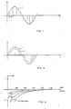
- an analogue, signal 1 is illustrated, and in this example it is sinusoidal. It has been sampled to give the sample values s 1 , S2 ..., which constitute the input signal to a digital filter.
- the output signal from the filter is illustrated in Figure 2.
- the sample values S1 S2 ... have been given a somewhat lower value than that of the nominal signal 1 due to truncations in the filter.
- the (dashed) analogue signal 2 corresponding to the truncated sample values S1 S2 ... is thus less than the signal 1.
- Figure 3 illustrates the amplification A in a filter as a function of the signal level. The number of bits/words (16, 17, 18 or 19 bits/words has been given as a parameter.
- the object of the present invention is to provide a method and a device which will compensate the error occurring in the truncation of a digital signal having a given number of bits/words, the signal being processed in a digital filter.
- the mean truncation error for the filter which processes the signal is calculated, this error being added to the positive input samples of the filter, and subtracted from the negative input samples.
- Figures 1, 2 and 3 have been explained hereinbefore in conjunction with the background art.
- Figure 4 is a time chart illustrating how, in accordance with the inventive method, an amount +e t is added to the positive signal samples s 1 , S2 ... and a negative amount -e t is added to the negative signal samples s 3 , S4 ... No correction is added to the signal sample s 5 which is zero.
- Figure 5 is a diagram of the output signal from the digital filter. Since the correction e t has been selected equal to the mean truncation error, the output signal samples follow on an average the desired nominal output signal 3.
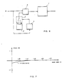
- FIG. 6 is a block diagram for a possible embodiment of a device included in a subscriber line audioprocessing circuit (SLAC), for example, and carries out the method according to the invention.
- a sampled signal is obtained at the output a, this signal not yet having been processed in any digital filter and is not truncated.
- This signal is to betaken to a main transmission filter 1 for filtering.
- the input a is connected to the first input of a digital adder circuit 2 and a digital sensing unit 4, which conventionally senses the polarity of the incoming signal at the input a.
- the block 3 is illustrated here as a simple memory unit, which stores the values +e t and -e t in digital form, the value +e t being obtained at the output b 1 and the value -e t at the output b 2 . Since the values ⁇ e, are generally represented by more than one bit, b 1 and b 2 represent the output from two bus lines.
- the block 5 is a controllable switch, e.g.
- a multiplexer which connects the output b 1 or b 2 to the second input of the adder circuit 2 in response to the output magnitude (0 or 1) obtained at the output of the sensing unit 4. If this unit senses positive polarity in the input signal at the input a, binary "one" is sent to the switch 5 and this connects the output b 1 to the second input of the adder circuit 2. On the other hand, if a negative polarity is sensed, a binary "zero" is sent and the switch is controlled so that the output b 2 is connected to the second input of the adder circuit. A value +e t is thus added to the incoming sampled signal, which is then taken to the digital filter 1.
- FIG. 7 is a diagram of the filter amplification as a function of the input signal level, when the compensating circuit according to Figure 6 is connected such as to precede the filter.
- the same amplification properties are achieved with 16 bits/word in the latter case with the inventive method as if about 19 bits/words were used without the inventive method being utilized.
- the improvement in the amplification linearity thus corresponds to a word length of several bits, and according to the above this gives simpler calculating circuits.
- the compensating circuit according to Figure 6 is illustrated in the form of a block diagram for the purpose of explanation and constitutes a possible embodiment.
- the various blocks memory unit, adding circuit, switches
- IC technique in the arithmetical unit ALU of the subscriber line circuit.
- the magnitude e t should be an integral number in the ALU. This generally results in that the compensation will not be entirely optimum.
Landscapes
- Engineering & Computer Science (AREA)
- Physics & Mathematics (AREA)
- Theoretical Computer Science (AREA)
- General Physics & Mathematics (AREA)
- Computer Hardware Design (AREA)
- Mathematical Physics (AREA)
- General Engineering & Computer Science (AREA)
- Mathematical Optimization (AREA)
- Pure & Applied Mathematics (AREA)
- Mathematical Analysis (AREA)
- Computing Systems (AREA)
- Computational Mathematics (AREA)
- Analogue/Digital Conversion (AREA)
- Dc Digital Transmission (AREA)
- Detection And Prevention Of Errors In Transmission (AREA)
- Interface Circuits In Exchanges (AREA)
- Transmission Systems Not Characterized By The Medium Used For Transmission (AREA)
- Complex Calculations (AREA)
- Noise Elimination (AREA)
- Radar Systems Or Details Thereof (AREA)
- Reduction Or Emphasis Of Bandwidth Of Signals (AREA)
- Electronic Switches (AREA)
- Facsimile Image Signal Circuits (AREA)
- Error Detection And Correction (AREA)
- Cable Transmission Systems, Equalization Of Radio And Reduction Of Echo (AREA)
- Apparatus For Radiation Diagnosis (AREA)
- Digital Transmission Methods That Use Modulated Carrier Waves (AREA)
- Analysing Materials By The Use Of Radiation (AREA)
- Optical Communication System (AREA)
- Data Exchanges In Wide-Area Networks (AREA)
Abstract
Description
- The present invention relates to a method and apparatus wherein a sampled signal with a given number of bits, e.g. 16 bits, is compensated for the error in the signal occurring when the signal is truncated towards a lower value after multiplication. Such an operation is generally performed in a digital filter.
- In a digital filter, particularly one included in a subscriber line audioprocessing circuit (SLAC), calculations are carried out on a sampled signal. Each signal sample is represented as a digital word in linear code. The number of bits/word depends on the dynamic range required by the filter.
- Multiplications with digital coefficients are performed in the calculations in the filter. The result of a multiplication normally contains more bits than the available word length, and the result must therefore be rounded off or truncated. By rounding off is intended here that the digital value is given a new value lying nearest over or under the original value, according to the same rules as those for decimals. By truncation is intended here magnitude truncation, i.e. the digital value is given a new value, the amount of which is always under the amount of the original value (truncation towards zero).
- If rounding off is used there is a risk of self-oscillation in the digital filter if this is of the infinite impulse response type, i.e. filter where the signal is fed back.
- If magnitude truncation is used, the filter can be constructed so that the risk of self-oscillation is removed, since the digital values are continually rounded off towards zero. Truncation is furthermore easier to realize than rounding off. However, magnitude truncation results in that the signal will always be somewhat too small, due to truncation errors in the calculations. This particularly affects the low signal levels where the truncation error is not negligible compared with the signal amplitude. In the accompanying Figure 1, an analogue,
signal 1 is illustrated, and in this example it is sinusoidal. It has been sampled to give the sample values s1, S2 ..., which constitute the input signal to a digital filter. The output signal from the filter is illustrated in Figure 2. Apart from the desired changes in the signal caused by filtering, the sample values S1 S2 ... have been given a somewhat lower value than that of thenominal signal 1 due to truncations in the filter. The (dashed)analogue signal 2 corresponding to the truncated sample values S1 S2 ... is thus less than thesignal 1. - It is previously known to increase the number of bits/words so that the effect of truncation errors will be as small as possible. Many bits/words result in a more complicated circuit, however, since registers, stores and calculating units, i.e. arithmatic logic units (ALU), must be made large. On the appended drawing, Figure 3 illustrates the amplification A in a filter as a function of the signal level. The number of bits/words (16, 17, 18 or 19 bits/words has been given as a parameter.
- The object of the present invention is to provide a method and a device which will compensate the error occurring in the truncation of a digital signal having a given number of bits/words, the signal being processed in a digital filter.
- In accordance with the invention, the mean truncation error for the filter which processes the signal is calculated, this error being added to the positive input samples of the filter, and subtracted from the negative input samples. The invention is defined in the following claims.
- The invention will now be described in detail with reference to the accompanying drawings.
- Figures 1 and 2 are diagrams of a sinusoidal, sampled signal before and after truncation of a digital filter;
- Figure 3 illustrates the amplification in a digital filter as a function of the input signal level for different word lengths;
- Figures 4 and 5 are diagrams corresponding to the diagrams in Figures 1 and 2 and are intended to illustrate the method in accordance with the invention;
- Figure 6 is a block diagram of a conceivable device in accordance with the invention;
- Figure 7 is the same diagram as in Figure 3, but the inventive method has now been used on the filter input signal.
- Figures 1, 2 and 3 have been explained hereinbefore in conjunction with the background art. Figure 4 is a time chart illustrating how, in accordance with the inventive method, an amount +et is added to the positive signal samples s1, S2 ... and a negative amount -et is added to the negative signal samples s3, S4 ... No correction is added to the signal sample s5 which is zero. Figure 5 is a diagram of the output signal from the digital filter. Since the correction et has been selected equal to the mean truncation error, the output signal samples follow on an average the desired
nominal output signal 3. - Figure 6 is a block diagram for a possible embodiment of a device included in a subscriber line audioprocessing circuit (SLAC), for example, and carries out the method according to the invention. A sampled signal is obtained at the output a, this signal not yet having been processed in any digital filter and is not truncated. This signal is to betaken to a
main transmission filter 1 for filtering. - The input a is connected to the first input of a
digital adder circuit 2 and a digital sensing unit 4, which conventionally senses the polarity of the incoming signal at the input a. Theblock 3 is illustrated here as a simple memory unit, which stores the values +et and -et in digital form, the value +et being obtained at the output b1 and the value -et at the output b2. Since the values ±e, are generally represented by more than one bit, b1 and b2 represent the output from two bus lines. The block 5 is a controllable switch, e.g. a multiplexer, which connects the output b1 or b2 to the second input of theadder circuit 2 in response to the output magnitude (0 or 1) obtained at the output of the sensing unit 4. If this unit senses positive polarity in the input signal at the input a, binary "one" is sent to the switch 5 and this connects the output b1 to the second input of theadder circuit 2. On the other hand, if a negative polarity is sensed, a binary "zero" is sent and the switch is controlled so that the output b2 is connected to the second input of the adder circuit. A value +et is thus added to the incoming sampled signal, which is then taken to thedigital filter 1. A calculation is performed in the filter with the aid of multipliers and adding circuits and truncations are carried out, an output signal being obtained having a signal sample illustrated in Figure 5, as well as the resulting analogue counterpart,curve 3. Figure 7 is a diagram of the filter amplification as a function of the input signal level, when the compensating circuit according to Figure 6 is connected such as to precede the filter. In comparison with the amplification according to Figure 3, it will be seen that the same amplification properties are achieved with 16 bits/word in the latter case with the inventive method as if about 19 bits/words were used without the inventive method being utilized. The improvement in the amplification linearity thus corresponds to a word length of several bits, and according to the above this gives simpler calculating circuits. - The compensating circuit according to Figure 6 is illustrated in the form of a block diagram for the purpose of explanation and constitutes a possible embodiment. In practice, the various blocks (memory unit, adding circuit, switches) are realised with IC technique in the arithmetical unit ALU of the subscriber line circuit.
- In order that compensation for the truncation error may be kept simple, the magnitude et should be an integral number in the ALU. This generally results in that the compensation will not be entirely optimum.
Claims (4)
Priority Applications (2)
| Application Number | Priority Date | Filing Date | Title |
|---|---|---|---|
| AT84904199T ATE30653T1 (en) | 1983-11-24 | 1984-10-31 | METHOD OF COMPENSATION FOR THE TAMPING ERROR IN A SAMPLE SIGNAL AND AN APPARATUS FOR CARRYING OUT THE METHOD. |
| MYPI87000944A MY100565A (en) | 1983-11-24 | 1987-07-04 | A method to compensate for the truncation error in a sampled signal and a device for carrying out the method |
Applications Claiming Priority (2)
| Application Number | Priority Date | Filing Date | Title |
|---|---|---|---|
| SE8306483A SE440300B (en) | 1983-11-24 | 1983-11-24 | PROCEDURE TO COMPENSATE IN A COMPLETE SIGNAL FOR TRUNCTION ERRORS AND DEVICE FOR EXECUTING THE PROCEDURE |
| SE8306483 | 1983-11-24 |
Publications (2)
| Publication Number | Publication Date |
|---|---|
| EP0162076A1 EP0162076A1 (en) | 1985-11-27 |
| EP0162076B1 true EP0162076B1 (en) | 1987-11-04 |
Family
ID=20353446
Family Applications (1)
| Application Number | Title | Priority Date | Filing Date |
|---|---|---|---|
| EP84904199A Expired EP0162076B1 (en) | 1983-11-24 | 1984-10-31 | A method to compensate for the truncation error in a sampled signal and a device for carrying out the method |
Country Status (22)
| Country | Link |
|---|---|
| US (1) | US4750146A (en) |
| EP (1) | EP0162076B1 (en) |
| KR (1) | KR900008410B1 (en) |
| AT (1) | ATE30653T1 (en) |
| AU (1) | AU569928B2 (en) |
| BR (1) | BR8407181A (en) |
| CA (1) | CA1248603A (en) |
| DE (1) | DE3467275D1 (en) |
| DK (1) | DK162868C (en) |
| ES (1) | ES537892A0 (en) |
| FI (1) | FI82795C (en) |
| GR (1) | GR80983B (en) |
| IE (1) | IE55857B1 (en) |
| IN (1) | IN161619B (en) |
| IT (1) | IT1177290B (en) |
| MX (1) | MX156872A (en) |
| MY (1) | MY100565A (en) |
| NO (1) | NO167348C (en) |
| PT (1) | PT79474B (en) |
| SE (1) | SE440300B (en) |
| WO (1) | WO1985002508A1 (en) |
| YU (1) | YU45678B (en) |
Families Citing this family (11)
| Publication number | Priority date | Publication date | Assignee | Title |
|---|---|---|---|---|
| JPH01169627A (en) * | 1987-12-25 | 1989-07-04 | Toshiba Corp | Highly accurate adding device |
| JP2957183B2 (en) * | 1988-07-29 | 1999-10-04 | 日本電気株式会社 | Cyclic digital filter |
| JP3199371B2 (en) * | 1990-07-30 | 2001-08-20 | 松下電器産業株式会社 | Rounding device |
| JPH04332215A (en) * | 1991-05-08 | 1992-11-19 | Matsushita Electric Ind Co Ltd | Offset remover |
| JP3103914B2 (en) * | 1992-08-21 | 2000-10-30 | ソニー株式会社 | Data rounding circuit and data restoration circuit |
| US5493343A (en) * | 1994-12-28 | 1996-02-20 | Thomson Consumer Electronics, Inc. | Compensation for truncation error in a digital video signal decoder |
| US5696710A (en) * | 1995-12-29 | 1997-12-09 | Thomson Consumer Electronics, Inc. | Apparatus for symmetrically reducing N least significant bits of an M-bit digital signal |
| US6253222B1 (en) * | 1998-10-31 | 2001-06-26 | Hewlett-Packard Company | Compression of limited range floating point numbers |
| US6240431B1 (en) * | 1998-10-31 | 2001-05-29 | Hewlett-Packard Company | Decompression of limited range floating point numbers |
| US6401107B1 (en) * | 1999-11-03 | 2002-06-04 | Motorola, Inc. | Method and processor for reducing computational error in a processor having no rounding support |
| US9450601B1 (en) | 2015-04-02 | 2016-09-20 | Microsoft Technology Licensing, Llc | Continuous rounding of differing bit lengths |
Family Cites Families (5)
| Publication number | Priority date | Publication date | Assignee | Title |
|---|---|---|---|---|
| US3891837A (en) * | 1972-07-03 | 1975-06-24 | Drew E Sunstein | Digital linearity and bias error compensating by adding an extra bit |
| US4195350A (en) * | 1978-06-19 | 1980-03-25 | Cbs Inc. | Method and apparatus for eliminating deadband in digital recursive filters |
| US4282581A (en) * | 1979-10-15 | 1981-08-04 | Sperry Corporation | Automatic overflow/imminent overflow detector |
| US4280196A (en) * | 1979-11-14 | 1981-07-21 | Hewlett-Packard Company | Correction of zero drift, gain drift, and distortion errors in analog storage devices |
| US4589084A (en) * | 1983-05-16 | 1986-05-13 | Rca Corporation | Apparatus for symmetrically truncating two's complement binary signals as for use with interleaved quadrature signals |
-
1983
- 1983-11-24 SE SE8306483A patent/SE440300B/en not_active IP Right Cessation
-
1984
- 1984-10-25 IN IN826/DEL/84A patent/IN161619B/en unknown
- 1984-10-30 KR KR1019840006773A patent/KR900008410B1/en not_active IP Right Cessation
- 1984-10-31 AU AU36131/84A patent/AU569928B2/en not_active Ceased
- 1984-10-31 DE DE8484904199T patent/DE3467275D1/en not_active Expired
- 1984-10-31 US US06/755,379 patent/US4750146A/en not_active Expired - Lifetime
- 1984-10-31 BR BR8407181A patent/BR8407181A/en not_active IP Right Cessation
- 1984-10-31 WO PCT/SE1984/000367 patent/WO1985002508A1/en active IP Right Grant
- 1984-10-31 EP EP84904199A patent/EP0162076B1/en not_active Expired
- 1984-10-31 AT AT84904199T patent/ATE30653T1/en not_active IP Right Cessation
- 1984-11-08 PT PT79474A patent/PT79474B/en not_active IP Right Cessation
- 1984-11-08 CA CA000467313A patent/CA1248603A/en not_active Expired
- 1984-11-12 MX MX203356A patent/MX156872A/en unknown
- 1984-11-20 GR GR80983A patent/GR80983B/en unknown
- 1984-11-21 IE IE2975/84A patent/IE55857B1/en not_active IP Right Cessation
- 1984-11-22 IT IT23695/84A patent/IT1177290B/en active
- 1984-11-22 YU YU197584A patent/YU45678B/en unknown
- 1984-11-23 ES ES537892A patent/ES537892A0/en active Granted
-
1985
- 1985-06-20 FI FI852458A patent/FI82795C/en not_active IP Right Cessation
- 1985-07-23 DK DK335385A patent/DK162868C/en not_active IP Right Cessation
- 1985-10-16 NO NO85854118A patent/NO167348C/en unknown
-
1987
- 1987-07-04 MY MYPI87000944A patent/MY100565A/en unknown
Also Published As
Similar Documents
| Publication | Publication Date | Title |
|---|---|---|
| EP0162076B1 (en) | A method to compensate for the truncation error in a sampled signal and a device for carrying out the method | |
| US4817047A (en) | Processing circuit capable of raising throughput of accumulation | |
| US4078250A (en) | Log-antilog conversion for a digital radar system | |
| EP0407962B1 (en) | Adaptive echo canceller | |
| JPS6360927B2 (en) | ||
| JPH05504242A (en) | Method and apparatus for converting digital signals to analog signals | |
| US4737925A (en) | Method and apparatus for minimizing a memory table for use with nonlinear monotonic arithmetic functions | |
| US5463571A (en) | Multi-nary OR logic device | |
| US5463572A (en) | Multi-nary and logic device | |
| KR100290194B1 (en) | Infinite Impulse Response Ghost Elimination System | |
| US6058404A (en) | Apparatus and method for a class of IIR/FIR filters | |
| JPH0519170B2 (en) | ||
| KR100526074B1 (en) | Apparatus and method for equalizer filter units responsive to 5-level inputs signals | |
| JPH067375B2 (en) | Arithmetic circuit | |
| JP2659232B2 (en) | High dimensional digital filter | |
| JP2546014B2 (en) | Digital signal processor | |
| JPS5952361A (en) | Arithmetic system for picture signal processing | |
| JPS61273008A (en) | Adaptive type transversal filter | |
| JPH065505B2 (en) | Arithmetic circuit | |
| JPS5853218A (en) | Digital filter | |
| KR940007927B1 (en) | Multiplication circuit of digital filter | |
| JPH051498B2 (en) | ||
| JPS6155689B2 (en) | ||
| JPS63157231A (en) | Exponent addition/subtraction circuit | |
| JPS6255727A (en) | Signal processing multiplier |
Legal Events
| Date | Code | Title | Description |
|---|---|---|---|
| PUAI | Public reference made under article 153(3) epc to a published international application that has entered the european phase |
Free format text: ORIGINAL CODE: 0009012 |
|
| 17P | Request for examination filed |
Effective date: 19850619 |
|
| AK | Designated contracting states |
Designated state(s): AT BE CH DE FR GB LI NL |
|
| 17Q | First examination report despatched |
Effective date: 19870123 |
|
| GRAA | (expected) grant |
Free format text: ORIGINAL CODE: 0009210 |
|
| AK | Designated contracting states |
Kind code of ref document: B1 Designated state(s): AT BE CH DE FR GB LI NL |
|
| REF | Corresponds to: |
Ref document number: 30653 Country of ref document: AT Date of ref document: 19871115 Kind code of ref document: T |
|
| REF | Corresponds to: |
Ref document number: 3467275 Country of ref document: DE Date of ref document: 19871210 |
|
| ET | Fr: translation filed | ||
| PLBE | No opposition filed within time limit |
Free format text: ORIGINAL CODE: 0009261 |
|
| STAA | Information on the status of an ep patent application or granted ep patent |
Free format text: STATUS: NO OPPOSITION FILED WITHIN TIME LIMIT |
|
| 26N | No opposition filed | ||
| PGFP | Annual fee paid to national office [announced via postgrant information from national office to epo] |
Ref country code: FR Payment date: 19980930 Year of fee payment: 15 |
|
| PGFP | Annual fee paid to national office [announced via postgrant information from national office to epo] |
Ref country code: DE Payment date: 19981002 Year of fee payment: 15 Ref country code: AT Payment date: 19981002 Year of fee payment: 15 |
|
| PGFP | Annual fee paid to national office [announced via postgrant information from national office to epo] |
Ref country code: CH Payment date: 19981019 Year of fee payment: 15 |
|
| PGFP | Annual fee paid to national office [announced via postgrant information from national office to epo] |
Ref country code: NL Payment date: 19981020 Year of fee payment: 15 |
|
| PGFP | Annual fee paid to national office [announced via postgrant information from national office to epo] |
Ref country code: BE Payment date: 19981021 Year of fee payment: 15 |
|
| PG25 | Lapsed in a contracting state [announced via postgrant information from national office to epo] |
Ref country code: LI Free format text: LAPSE BECAUSE OF NON-PAYMENT OF DUE FEES Effective date: 19991031 Ref country code: CH Free format text: LAPSE BECAUSE OF NON-PAYMENT OF DUE FEES Effective date: 19991031 Ref country code: BE Free format text: LAPSE BECAUSE OF NON-PAYMENT OF DUE FEES Effective date: 19991031 Ref country code: AT Free format text: LAPSE BECAUSE OF NON-PAYMENT OF DUE FEES Effective date: 19991031 |
|
| BERE | Be: lapsed |
Owner name: TELEFON A.B. L M ERICSSON Effective date: 19991031 |
|
| PG25 | Lapsed in a contracting state [announced via postgrant information from national office to epo] |
Ref country code: NL Free format text: LAPSE BECAUSE OF NON-PAYMENT OF DUE FEES Effective date: 20000501 |
|
| REG | Reference to a national code |
Ref country code: CH Ref legal event code: PL |
|
| PG25 | Lapsed in a contracting state [announced via postgrant information from national office to epo] |
Ref country code: FR Free format text: LAPSE BECAUSE OF NON-PAYMENT OF DUE FEES Effective date: 20000630 |
|
| NLV4 | Nl: lapsed or anulled due to non-payment of the annual fee |
Effective date: 20000501 |
|
| PG25 | Lapsed in a contracting state [announced via postgrant information from national office to epo] |
Ref country code: DE Free format text: LAPSE BECAUSE OF NON-PAYMENT OF DUE FEES Effective date: 20000801 |
|
| REG | Reference to a national code |
Ref country code: FR Ref legal event code: ST |
|
| PGFP | Annual fee paid to national office [announced via postgrant information from national office to epo] |
Ref country code: GB Payment date: 20011004 Year of fee payment: 18 |
|
| REG | Reference to a national code |
Ref country code: GB Ref legal event code: IF02 |
|
| PG25 | Lapsed in a contracting state [announced via postgrant information from national office to epo] |
Ref country code: GB Free format text: LAPSE BECAUSE OF NON-PAYMENT OF DUE FEES Effective date: 20021031 |
|
| GBPC | Gb: european patent ceased through non-payment of renewal fee |