EP0161496B1 - Digital magnetic recording circuit - Google Patents
Digital magnetic recording circuit Download PDFInfo
- Publication number
- EP0161496B1 EP0161496B1 EP85104458A EP85104458A EP0161496B1 EP 0161496 B1 EP0161496 B1 EP 0161496B1 EP 85104458 A EP85104458 A EP 85104458A EP 85104458 A EP85104458 A EP 85104458A EP 0161496 B1 EP0161496 B1 EP 0161496B1
- Authority
- EP
- European Patent Office
- Prior art keywords
- input terminal
- circuit
- voltage
- switching elements
- record
- Prior art date
- Legal status (The legal status is an assumption and is not a legal conclusion. Google has not performed a legal analysis and makes no representation as to the accuracy of the status listed.)
- Expired
Links
- 230000000295 complement effect Effects 0.000 claims description 11
- 230000004044 response Effects 0.000 claims description 11
- 239000003990 capacitor Substances 0.000 claims description 6
- 239000004065 semiconductor Substances 0.000 claims description 4
- 229910044991 metal oxide Inorganic materials 0.000 claims description 2
- 150000004706 metal oxides Chemical class 0.000 claims description 2
- 238000010276 construction Methods 0.000 description 17
- 239000010409 thin film Substances 0.000 description 17
- 238000010586 diagram Methods 0.000 description 9
- 229920006227 ethylene-grafted-maleic anhydride Polymers 0.000 description 7
- 230000004907 flux Effects 0.000 description 6
- 230000005540 biological transmission Effects 0.000 description 5
- 239000004020 conductor Substances 0.000 description 5
- 238000004519 manufacturing process Methods 0.000 description 5
- 238000004804 winding Methods 0.000 description 5
- 238000005516 engineering process Methods 0.000 description 4
- 230000001939 inductive effect Effects 0.000 description 4
- 239000011295 pitch Substances 0.000 description 2
- 230000001737 promoting effect Effects 0.000 description 2
- 239000007787 solid Substances 0.000 description 2
- 230000005236 sound signal Effects 0.000 description 2
- 229910000859 α-Fe Inorganic materials 0.000 description 2
- 125000003345 AMP group Chemical group 0.000 description 1
- 230000002146 bilateral effect Effects 0.000 description 1
- 230000008094 contradictory effect Effects 0.000 description 1
- 238000005520 cutting process Methods 0.000 description 1
- 230000007423 decrease Effects 0.000 description 1
- 230000001419 dependent effect Effects 0.000 description 1
- 230000001627 detrimental effect Effects 0.000 description 1
- 230000000694 effects Effects 0.000 description 1
- 230000006872 improvement Effects 0.000 description 1
- 238000000034 method Methods 0.000 description 1
- 238000012986 modification Methods 0.000 description 1
- 230000004048 modification Effects 0.000 description 1
- 230000000135 prohibitive effect Effects 0.000 description 1
- 238000005070 sampling Methods 0.000 description 1
- 230000007704 transition Effects 0.000 description 1
- 238000001771 vacuum deposition Methods 0.000 description 1
Images


Classifications
-
- G—PHYSICS
- G11—INFORMATION STORAGE
- G11B—INFORMATION STORAGE BASED ON RELATIVE MOVEMENT BETWEEN RECORD CARRIER AND TRANSDUCER
- G11B20/00—Signal processing not specific to the method of recording or reproducing; Circuits therefor
- G11B20/10—Digital recording or reproducing
- G11B20/10527—Audio or video recording; Data buffering arrangements
-
- G—PHYSICS
- G11—INFORMATION STORAGE
- G11B—INFORMATION STORAGE BASED ON RELATIVE MOVEMENT BETWEEN RECORD CARRIER AND TRANSDUCER
- G11B20/00—Signal processing not specific to the method of recording or reproducing; Circuits therefor
- G11B20/10—Digital recording or reproducing
-
- G—PHYSICS
- G11—INFORMATION STORAGE
- G11B—INFORMATION STORAGE BASED ON RELATIVE MOVEMENT BETWEEN RECORD CARRIER AND TRANSDUCER
- G11B5/00—Recording by magnetisation or demagnetisation of a record carrier; Reproducing by magnetic means; Record carriers therefor
- G11B5/02—Recording, reproducing, or erasing methods; Read, write or erase circuits therefor
- G11B5/09—Digital recording
Definitions
- the present invention relates to a digital magnetic recording circuit and, more particularly, to a digital magnetic recording circuit for use with a pulse code modulation recording and playback apparatus as set forth in the preamble of claim 1.
- a digital magnetic recording circuit for use with a pulse code modulation recording and playback apparatus as set forth in the preamble of claim 1.
- Such circuit is known from EP-A-0 012 264.
- a pulse code modulation (PCM) recording and playback apparatus is constructed to convert audio and other analog signals to digital ones so as to record and reproduce the digital signals into and out of a suitable recording medium, e.g. magnetic recording medium.
- PCM recording and playback apparatuses may generally be classified into two types by the recording and playback system, i.e., one which uses stationary heads and the other which uses rotary heads.
- the stationary head type system As to the stationary head type system, assuming that audio signals are transmitted over two transmission channels, with sixteen transmission bits per channel and at a sampling frequency of 44.1 kiloherts or above, the total transmission rate of the audio signals is as high as 2 megabits per second (MBPS) or above.
- MBPS megabits per second
- the primary requisite for stable recording and playback is, therefore, providing a plurality of tracks and designing the transmission rate per track adequately low.
- the stationary head type system needs to perform recording and playback relying on a plurality of tracks, i.e. multi-track recording and playback. Meanwhile, the multi-track recording and playback may be accomplished by means of conventional winding type record heads.
- a prior art multi-track record head is shown together with a magnetic tape T.
- Multi-tracks ch 1 -ch n (only ch 1 and ch n are shown) are formed in the magnetic tape T in n data channels.
- a record signal input terminal 10a is interconnected to a record amplifier circuit A 1 , while a record signal input terminal 10b is connected to ground.
- n record amplifier circuits A 1 in total each having the construction shown in Fig. 1, i.e. record amplifier circuits A 1 ⁇ A n (only A 1 is shown).
- each of the record amplifier circuits A 1 ⁇ A n comprises an operational amplifier (OP AMP) 12 and resistors R 1 ⁇ R 5 and serves as a known drive circuitwell known in the art.
- the multi-track record head comprises record heads M 1 ⁇ M n (only M 1 and M n are shown) which are connected at one end to their associated record amplifier circuits A 1 ⁇ A n and at the other end to ground.
- digital signals, or data are recorded as flux reversals in the tape T by applying positive and negative signal voltages to the record signal input terminals 10a and 10b, respectively.
- the heads M 1 ⁇ M n are individually applied with positive and negative constant currents i such as shown in Fig. 2 from their associated record amplifier circuits A 1 ⁇ A n , the constant current applied to the record head M 1 , for example, being expressed as: where e is the voltage applied to the record amplifier circuit A i , R,-R 4 are the resistance values of the resistors included in the circuit A i , and R, is equal to R 4 .
- Fig. 2 illustrating an exemplary waveform of current applied to each record head
- the abscissa represents time t and the ordinate, current i.
- the current i increases upwardly along the ordinate and decreases downwardly along the same.
- ZEROs and ONEs shown above the waveform are indicative of the kinds of digital signals to be recorded into the tape T.
- each of the record amplifier circuits A,-An is a constant current circuit producing constant positive and negative current, generally referred to as a bilateral circuit.
- each record amplifier circuit, A,-An requires two separate power source circuits to be supplied with positive and negative source voltages and, in addition, the same number of large current output OP AMPs as the data channels are indispensable.
- the number of record amplifiers A 1 ⁇ A n increases with that of data channels. This undesirably adds to the total circuitry scale and, thereby, increases power consumption and costs while obstructing the trend to a small-size lightweight construction.
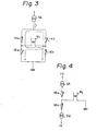
- Fig. 3 shows a drive circuit of the type using a balanced transformerless (BTL) circuit and a constant current source in combination such drive circuit is shown in aforementioned EP-A-0 012 264
- Fig. 4 shows a drive circuit implemented by positive and negative current sources in a complementary symmetry circuit.
- the drive circuit in any of Figs. 3 and 4 is associated with the data channel ch, only by way of example.
- the drive circuit in Fig. 3 comprises a constant current source SA and semiconductor switching elements 14a, 14b, 16a and 16b which may comprise, for example, metal oxide semiconductor (MOS) transistors or bipolar transistors.
- the switching elements 14a and 16a behave in a reciprocal manner and so do the switching elements 14b and 16b. That is, while the switching element 14a is conductive, the switching element 14b is nonconductive, the switching element 16a is nonconductive, and the switching element 16b is conductive (the condition illustrated in Fig. 3). So controlling the states of the switching elements 14a, 14b, 16a and 16b causes a forward current and a reverse current to selectively flow through the magnetic head M i , enabling data to be recorded as flux reversals in the tape T.
- MOS metal oxide semiconductor
- the drive circuit comprises a positive constant current source SA, a negative constant current source SB, and semiconductor switching elements 18a and 18b which may comprise MOS transistors or bipolar transistors, for example.
- the switching elements 18a and 18b operate reciprocal to each other, that is, while the former is conductive, the latter remains nonconductive (the condition shown in Fig. 4).
- By controlling the states of the switching elements 18a and 18b in the described manner it is possible to conduct forward and reverse currents selectively through the head M i , allowing flux reversals to be recorded in the tape T.
- the drive circuits shown in Figs. 3 and 4 share the same recording principles, i.e. switching the direction of current flowing through a head by means of a switching element of the kind mentioned.
- the problem is, however, that resistance is constantly preserved in a switching element because an ideal switching element whose resistance in a conductive state is zero ohm is impractical. Due to such resistance, switching elements used to control the currents for driving the head brings about power losses.
- This problem is particularly serious in the drive circuit of Fig. 3 in which four switching elements are required to drive a single record head and two of them are constantly introduced into the current path leading to the record head, further promoting the power loss. In a multi-track head configuration, the number of switching elements and, therefore, the circuit scale would become prohibitive as well as the costs and power loss.
- thin-film magnetic heads enhances the ease of production of multi-track thin-film heads because they are implemented by pattern mask technologies extensively used in the integrated circuit fabrication art and others. Yet, considering the interconnections of the heads to drive circuits and the number of bonding steps involved in the production, that is, the productivity of thin-film magnetic heads, it is desirable that thin-film heads be commonly interconnected by a pattern mask as far as possible. In this respect, the drive circuit of Fig. 3 cannot have its two terminals commonly connected in providing a multi-track head configuration, except at the cost of a greater number of wiring steps.
- the drive circuit of Fig. 4 is smaller than that of Fig. 3 in the number of switching elements per data channel as well as in the number of switching elements disposed in the current path to the record head, successfully cutting down the power loss.
- the current source should preferably comprise a constant current source implemented by an electronic circuit and, in a multi-track head configuration with the drive circuit of Fig. 4, the constant current source needs be associated with each record head. This, coupled with the fact that two separate current sources are necessary per data channel, would boost the circuitry scale to a critical extent in a multi-track configuration.
- a constant current source or a constant voltage source is often constructed to attain a desired constant current or voltage characteristic by applying surplus power during light load operations to a control transistor or the like as power losses. Then, the source capacity of a drive circuit inclusive of such power losses becomes much greater than the power which is expected to be consumed by the record head and switching elements.
- a constant current or voltage source of the above-described nature is contradictory to the growing demand for a small-size, lightweight and cost-effective construction, particularly in the home-use equipment market.
- a dc power source circuit made up simply of a small-capacity power source transformer, a rectifier and an electrolytic capacitor is used in many applications. Where such a dc power source circuit is used and if its power source capacity is small, an increase in load results in a significant drop of voltage which in turn makes it difficult to supply a predetermined current to the record head.
- This object is attained by the characterizing features of claim 1.
- Preferred embodiments of the invention are subject matter of the dependent claims.
- a digital magnetic recording circuit for a recording and playback apparatus which records input digital signals into a plurality of tracks formed in a recording medium.
- the circuit changes the potential at a common junction of record heads in response to input digital data.
- a single control circuit suffices to apply a constant current to each record head with no regard to input digital data.
- the number of switching elements per track is reduced to in turn reduce power losses attributable to switching elements.
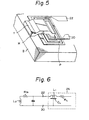
- the thin-film magnetic record head comprises terminals 20 and 22 for electrical connection, a coil pattern P, a yoke Y, and a ferrite base B.
- An air gap H is defined between the yoke Y and the ferrite base B.
- a conventional winding (bulk) type record head which has winding around a core
- a multi-track record head whose track pitches are on the order of several tens of microns.
- the available number of turns of the winding is smaller in the thin-film head than in the bulk type head, the former cannot serve the recording application unless the recording current is boosted.
- the number of turns may be increased in order to suppress the recording current, the number of turns available with a thin-film record head is not more than several, several tens of turns are impracticable without resorting to microtechniques such as pattern bridging which are detrimental to productivity.
- a thin-film magnetic head facilitates the production of a multi-track head with any desired track pitches, but the number of turns attainable therewith is small.
- Fig. 6 shows an equivalent circuit of a thin-film head of the above-mentioned nature.
- the equivalent circuit includes the terminals 20 and 22 shown in Fig. 5, a lead 24 for electrical connection, a coil inductance L, of the lead 24, an inductance L 2 of the head, a conductor resistance Rm of the head, a capacitance Cm of the head, a conductor resistance RL of the lead 24, and a capacitance CL of the lead 24.
- the coil inductance H, capacitance CL and conductor resistance RL of the lead 24 grow to unnegligible degrees, while the inductance L 2 of the head is not so great.
- the value of the conductor resistance Rm of the head constitutes a major load as viewed from the drive circuit side. That is, while the conventional bulk type head provides an inductive load, the thin- head magnetic head constitutes an inductive load rather close to a conductor resistance load. What this implies is that a drive circuit for operating a thin-film magnetic head needs only be construct provide a predetermined large current.
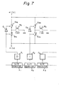
- Fig. 7 is a block diagram showing a basic construction of a drive circuit applicable to one embodiment of the present invention.
- multi-track record heads M 1 , M 2 ... which are implemented by thin-film magnetic heads.
- the heads M 1 , M 2 ... are commonly interconnected at one end thereof and supplied with a predetermined potential (grounded in Fig. 7 for simplicity).
- the other end of the head M 1 is connected to a junction of switching elements S 1a and S 1b , that of the head M 2 to a junction of switching elements S 2a and S 2b , and so on. All such switching elements comprise commonly connected MOS transistors or the like.
- a positive voltage, +1 volt for example, is applied across the switching elements S ia , S 2a ..., and a negative voltage, -1 volt for example, across the switching elements S ib , S 2b ....
- the switching elements S ia , S ib , S 2a , S 2b and so on are connected in serial pairs which are associated in one-to-one correspondence with the tracks.
- the switching elements S 1a , S 2a ... respectively are controlled by output signals of flip-flops F 1 , F 2 and so on by way of inverters G 1 , G 2 ....
- the other switching elements S 1b , S 2b ... are controlled directly by the output signals of the flip-flops F 1 , F 2 ..., respectively.
- the switching elements S 1a and S 1b behave in a reciprocal fashion; while the switching elements S 1a is conductive, the switching element S 1b remains nonconductive and, while the former is nonconductive, the latter remains conductive.
- the construction is such that while the flip-flop F 1 produces a (logical) ZERO and the flip-flop F 2 a ONE, the switching element S 1a is held nonconductive, the switching element S lb conductive, the switching element S 2a conductive, and the switching element S 2b nonconductive.
- the same principle of reciprocal actions applies to the other switching elements.
- each of the switching elements exerts resistance of 1 ohm when turned on, and that as mentioned earlier a voltage of +1 volt is applied across each switching element S ia , S 2a , ..., and a voltage of -1 volt across each switching element S ib , S 2b ....
- a current of 1 ampere flows through the head M 1 as indicated by a leftwardly headed arrow, that is, from the ground toward the switching element S ib
- a current of 1 ampere flows through the head M 2 as indicated by a rightwardly headed arrow, that is, from the switching element S 2a toward ground.
- the supply of 7-watt power to the switching elements S 1a , S 2a ... and the supply of 3- watt power to the other switching elements S 1b , S 2b ... may be implemented if the switching elements S ia , S 2a ... and the switching elements S ib , S 2b are commonly supplied with the same power source voltage, and the junction of the record heads, which is grounded in Fig. 7, is kept at a negative potential instead of the illustrated ground potential.
- Such will control the proportion of the positive and negative power delivery and, thereby, ensure the supply of a substantially constant desired current to the record heads.
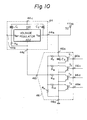
- a digital magnetic recording circuit embodying the present invention is shown and generally designated by the reference numeral 30.
- the recording circuit in this particular embodiment is assumed to use a four-track recording head by way of example.
- the switching elements 36, 38, 40 and 42 respectively are connected at the other end to one end of switching elements 36a, 38a, 40a and 42a and, via terminals 50a, 50b, 50c and 50d of a record head group 48, to one end of record heads 52, 54, 56 and 58.
- the other end of each record head 52, 54, 56 or 58 is connected to an output terminal 44b of the variable voltage drive circuit 44 via a terminal 50e.
- the other end of each switching element 36a, 38a, 40a or 42a and a terminal 44c of the drive circuit 44 are connected to ground.
- a terminal 60 to which a latch clock signal LK is applied, is connected to clock input terminals C of D flip-flops (D F/F) 64, 66, 68 and 70 which constitute a flop-flop (F/F) group 62, a reset terminal of a counter 72, and a clock input terminal of a latch circuit 74.
- Output terminals Q of the D F/Fs 64, 66, 68 and 70 respectively are led to control terminals of the switching elements 36, 38, 40 and 42, and output terminals Q to control terminals of the switching elements 36a, 38a, 40a and 42a.
- a terminal 76 to which serial digital data SD are applied, is connected to a serial data input terminal D of a serial-to-parallel (S/P) register 80 which is included in a register group 78.
- the terminal 76 is also connected to one input terminal of a two-input AND gate 82, which will produce a ONE only when supplied with ONEs at the same time.
- a terminal 84 where a clock pulse signal CK arrives is connected to transfer clock input terminals of S/P registers 86, 88 and 90 in the register group 78 as well as that of the S/P register 80, and to the other input terminal of the AND gate 82.
- the output terminal of the AND gate 82 is connected to a clock input terminal of the counter 72.
- Parallel output terminals of the counter 72 are commonly connected to data input terminals of the latch 74.
- Data output terminals of the latch 74 in turn are connected to data input terminals 46b, 46c, 46d and 46e of the voltage programmer 46.
- An output terminal 46f of the voltage programmer 46 is connected to a control terminal 44d of the variable voltage drive circuit 44, while a terminal 46g of the voltage programmer 46 is connected to ground.
- a parallel output terminal Q of the S/P register 80 is connected to a data input terminal D of the D F/F 64 as well as to a serial input terminal D of the S/P register 86.
- a parallel output terminal Q of the S/P register 86 is connected to a data input terminal D of the D F/F 66 as well as to a serial input terminal D of the S/P register 88.
- a parallel output terminal Q of the S/P register 88 is connected to a data input terminal D of the D F/F 68 and to a serial input terminal Dof the S/P register 90.
- a parallel input terminal Q of the S/P register 90 is connected to a data input terminal D of the D F/F 70.
- All the switching elements 36, 38, 40, 42, 36a, 38a, 40a and 42a comprise electronic switches such as MOS transistors and are controlled by signals which are applied thereto from the F/F group 62 by way of a level shifter and other interfaces, which are not shown in Fig. 8 and will be described later. Specifically, they are controlled such that the switching elements 36, 38, 40 and 42 and the switching elements 36a, 38a, 40a and 42a respectively are turned on by TTL level ONEs output from the output terminals Q and Q of the D F/Fs 64, 66, 68 and 70, and turned off by ZEROs.
- the terminals 32, 60, 76 and 84 constitute an input terminal group 92.
- variable voltage drive circuit 44 voltage programmer 46, counter 72, latch 74, and AND gate 82 constitute a common drive circuit (control drive circuit) 94 which is physically separate from the switching element group 34, record head group 48, FF group 62, register group 78, and input terminal group 92 and is externally located.
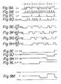
- four-track serial digital data SD are applied to the terminal 76 as shown in Fig. 9A by way of example.
- the digital data shown in Fig. 9A serially arrive in the order of the fourth track, the third track, the second track and the first track as indicated by numerals 4, 3, 2 and 1 above the waveform.
- the digital data SD are routed to the serial input terminal D of the S/P register 80.
- a clock pulse signal CK as shown in Fig. 9B.
- the clock pulse signal CK is fed to the transfer clock input terminals of the S/ P registers 80, 86, 88 and 90.
- the S/P registers 80, 86, 88 and 90 sequentially transfer the serial digital data, which are applied to their serial data input terminals D, serially from their parallel output terminals Q. That is, the serial digital data SD come in through the terminal 76 are sequentially transferred from the parallel output terminals of the S/P registers 80, 86, 88 and 90 as shown in Figs. 9E-9H.
- the latch clock signal LK arrived at the terminal 60 may have a waveform as shown in Fig. 9C.
- the signal LK is routed to the clock input terminals C of the D F/Fs 64, 66, 68 and 70.
- the data signals shown in Figs. 9E-9H respectively are applied to the data input terminals D of the D F/Fs 64, 66, 68 and 70.
- the D F/Fs 64, 66, 68 and 70 produce respectively the data signals shown in Figs. 9E-9H as data signals shown in Figs. 91-9L from their output terminals Q.
- Appearing at the output terminals Q of the D F/Fs 64, 66, 68 and 70 are inverted versions of such data signals as those shown in Figs. 91-9L.
- the switching elements 36, 38, 40 and 42 and the switching elements 36a, 38a, 40a and 42a individually become conductive when their associated D F/Fs in the F/F group 62 produces ONEs and nonconductive if otherwise.
- the AND gate 82 provides AND of the serial digital data SD shown in Fig. 9A and the clock pulse signal CK shown in Fig. 98, the AND being shown in Fig. 9D.
- the output of the AND gate 82 is routed to the clock input terminal of the counter 72 which then counts the input pulses.
- the output of the counter.72 is fed from the parallel output terminals of the counter to the data input terminals 46b, 46c, 46d and 46e of the voltage programmer 46 via the latch 74.
- the voltage programmer 46 In response to an output signal of the latch 74 (count from the counter 72), the voltage programmer 46 generates a control signal which will cause the variable voltage drive circuit 44 to apply voltages c as shown in Fig. 9M to the record head group 48.
- the record head group 48 is fabricated using thin films or the like, the commonly connected portions of the record heads can be wired by pattern mask techniques in the production line and, hence, the number of terminal wiring steps is reduced to (n+1) in the case of an n-track integrated magnetic head, which is a remarkable improvement over the prior art multi-track head configurations.
- the potential at the common junction of the record head group 48 is'varied in response to an input serial data signal. by counting only ONEs of AND of a serial data signal applied to the terminal 76 and a clock pulse signal applied to the terminal 84, thereby constantly supplying the record head group 48 with a predetermined current. Yet, the construction would become simpler if the input data signals were applied in parallel. Specifically, parallel data signals would permit the use of even analog demodulators such as a pulse counting detector.
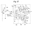
- variable voltage drive circuit 44 and that of the voltage programmer 46 included in the recording circuit 30 of Fig. 8 are shown.
- the same structural elements as those shown in Fig. 8 are designated by like reference numerals and will not be described in detail for simplicity.
- the terminal 32 is connected to the source input terminal 44a of the variable voltage drive circuit 44 and to the source input terminal 46a of the voltage programmer 46.
- the data input terminals 46b, 46c, 46d and 46e respectively are connected to bases of the transistors T" T 2 , T 3 and T 4 .
- the source input terminal 46a is connected via a capacitor C 3 to emitters of the transistors T 1 , T 2 , T 3 and T 4 as well as to the terminal 46g.
- Collectors of the transistors T i , T 2 , T 3 and T 4 are connected to the output terminal 46f via resistors R 7 , R 8 , R 9 and R 1o , respectively.
- the output terminal 46f is connected to the terminal 46g via a resistor R ii .
- the output terminal 46f of the voltage programmer 46 is connected to the control terminal 44d of the drive circuit 44.
- the control terminal 44d in turn is connected to an adjust (ADJ) terminal of the variable voltage regulator 100 and, via a resistor R s , to the output terminal 44b and an output terminal of the voltage regulator 100.
- the output terminal of the voltage regulator 100 is connected to the terminal 44c via a capacitor C i .
- the source input terminal 44a is connected to an input terminal of the voltage regulator 100 and, via a capacitor C 2 , to the terminal 44c.
- the voltage programmer 46 serves as a resistor switching circuit and is constructed such that the resistance between the source input terminal 46a and the output terminal 46f is variable depending data signals applied to the data input terminals 46b, 46c, 46d and 46e.
- the variable voltage regulator 100 functions to vary the resistance between the source input terminal 46a and output terminal 46f of the voltage programmer 46, thereby varying the output voltage.
- a power source voltage complementary to data signals applied to the data input terminals 46b, 46c, and 46e appear at the output terminal of the drive circuit 44.
- FIG. 11 alternative constructions of the variable voltage drive circuit 44 and voltage programmer 46 are shown.
- the terminal 32 is connected to the source input terminal 44a of the variable voltage drive circuit 44 and to the source input terminal 46a of the voltage programmer 46.
- the data input terminals 46b, 46c, 46d and 46e of the voltage programmer 46 are each connected to an input terminal of a digital-to-analog converter (DAC) 110, while the source input terminal 46a is connected to the DAC 110.
- the terminal 46g is connected to the DAC 110.
- the output terminal of the DAC 110 is connected to the output terminal 46f of the voltage programmer 46.
- the output terminal 46f of the voltage programmer 11 is connected to the control terminal 44d of the drive circuit 44.
- the control terminal 44d is connected to a non- . inverting input terminal of an OP AMP 112.
- the output terminal of the OP AMP 112 is connected to output terminal 44b of the drive circuit 44 as well as to an inverting input terminal of the OP AMP 112.
- Both the source input terminal 44a and terminal 44c are connected to the OP AMP 112.
- the voltage programmer 46 transforms digital data signals applied to its data input terminals 46b, 46c, 46d and 46e to analog data signals.
- the output voltage of the voltage programmer 46 is routed through the output terminal 46f and the control terminal 44d of the drive circuit 44 to the non-inverting input of the OP AMP 112, with the result that a source voltage corresponding to the data applied to the data input terminals 46b, 46c, 46d and 46e appears at the output terminal of the drive circuit 44.
- the recording circuit 30 needs a high-speed power source circuit capable of supplying a large current for each transmission bit and, also, a power source circuit and an operational amplifier the settling times of which sufficiently match with the required high-speed operations. It has been confirmed that the adjustable voltage drive circuit 44 and voltage programmer 46 provide desirable effects if implemented by discrete high-power power operational amplifiers or high-speed digital-to-analog converters.
- FIG. 12 there are shown specific examples of the switching element group and drive circuit associated therewith which are included in the recording circuit of Fig. 8.
- the construction shown in Fig. 12 focuses on switching elements 120 and 120a of the switching element group 48 by way of example.
- the same structural elements as those shown in Fig. 8 are designated by like reference numerals and detailed description thereof will be omitted for simplicity.
- the switching elements 120 and 120a which serve as the switching elements 42 and 42a of Fig. 8 comprise N-channel MOS transistors which are operated by a single power source.
- a power source voltage (+VDD) is applied to the drain of the switching element, or transistor, 120.
- the source of the transistor 120 is connected to the drain of the other switching element, or transistor, 120a, the junction of the two transistors 120 and 120a being connected to one end of the record head 58.
- the source of the transistor 120a is connected to ground.
- the source voltages applied to the gates of the transistors 120 and 120a need only be opposite in phase to each other and satisfy the following relation between the source voltage (+VDD) applied to the drain of the transistor 120 and a source voltage (+Vdd) applied to a complementary follower 122, which will be described:
- a level detector 124 is connected to the parallel output terminal Q of the S/P register 90 shown in Fig. 8, at which output signals appear with TTL levels (+5 volts and 0 volt).
- the level detector 124 functions to detect those of the output signals which are lower than, for example, 1.4 volts as ZEROs and those higher than, for example, 2.4 volts as ONEs.
- the level detector 124 may comprise transistors T 5 , T 6 and T 7 , diodes D l -D 7 , resistors R 12 ⁇ R 17 . and a switch 126.
- Signals detected by the level detector 124 are transferred to a level shifter 128 which, as shown in Fig. 12, is made up of MOS transistors MT, and MT 2 , and transistors T 8 and Tg.
- the output of the level shifter 126 is fed to the complementary follower 122.
- the function assigned to the complementary follower 122 is applying voltages of opposite phases to the gates of the transistors 120 and 12'Oa, which are MOS transistors as mentioned earlier.
- the complementary follower 122 serves to apply ground potential (source voltage +Vdd) in response to a ONE inputted to the level detector 124.
- the complementary follower 122 comprises transistors T,o, T " , T 12 and T 13 .
- the junction of the emitter of the transistor T jo and that of the transistor T" is connected to the gate of the transistor 120, while the junction of the emitter of the transistor T 12 and that of the transistor T 13 is connected to the gate of the transistor 120a.
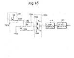
- the switching element group 34 and its associated drive circuit may be designed as shown in Fig. 13.
- Fig. 13 the illustration focuses to switching elements 130 and 130a of a switching element group, and the same structural elements as those shown in Fig. 12 are designated by like reference numerals.
- the switching elements 42 and 42a shown in Fig. 8 are implemented by N-channel MOS transistors 130 and 130a by way of example.
- the drain of the transistor 130 is connected to the drain of the transistor 130a, while their junction is connected to one end of the record head 58.
- a source voltage +VDD is applied to the source of the transistor 130, and a source voltage -VDD to the source of the transistor 130a. That is, the objective will be achieved if a source voltage +Vdd or (-Vdd) is applied to the gates of the transistors 130 and 130a under a condition:
- the level detector 124 and level shifter 128 shown in Fig. 13 are identical with those shown in Fig. 12 and, therefore, description thereof will be omitted.
- the gates of the transistors 130 and 130a are commonly connected.
- the complementary follower 122a therefore, needs only to control the commonly connected gates of the transistors 130 and 130a, accomplishing a simpler construction than the complementary follower 122 of Fig. 12. Such leads to simplification of the overall arrangement of the drive circuit associated with the switching element group 48.
- variable voltage drive circuit 44 will sequentially set and output a predetermined voltage for each bit period of sequentially transmitted digital data. Stated another way, it will serve as a constant voltage circuit having a low impedance characteristic.
- the record head group 48 is constructed by the use of thin films or the like so that, as viewed from the drive circuit 44 side, it exhibits a characteristic more resembling a resistive load than to an inductive load.
- Such record head group 48 has a pattern inductance which is apt to make the load obstruct the flow of high frequency components to the record head group 48.
- a parallel connection of a resistor R 18 and a capacitor C 4 may be connected between the outputterminal of the drive circuit 44 and the terminal 50e of the record head group 48 to serve as a compensation circuit 140.
- the implementation shown in Fig. 14 is effective to cause a current to flow in a more constant stable manner through the record head group 48, as indicated by a solid curve in Fig. 15.
- a current flows through the record head group 48 along a solid curve if the compensation circuit 140 of Fig. 14 is installed, and along a dotted curve if otherwise.
- Waveforms shown in Figs. 16A and 16B demonstrate respectively the operation of the prior art recording circuit whose current capacity is insufficient and the operation of the recording circuit 30 in accordance with the present invention.
- the abscissa shows time base and the ordinate, recording current.
- the recording circuit 30 in the illustrative embodiment is successful in supplying record heads with substantially constant recording currents.
- the present invention provides a digital magnetic recording circuit which applies constant current to recording heads with no regard to incoming digital data, reduces the number of required switching elements per track and, thereby, power losses attributable to switching elements, cuts down the number of wiring steps, and makes it needless to install a current source or voltage source for each track, thereby promoting a small-size, lightweight and inexpensive construction.
- the F/F group 62 shown in Fig. 8 may be combined with another such F/F group and so may be done each of the other associated circuits such as the variable voltage drive circuit.
- the two independent systems may be switched from one to the other by a high-speed switching element in order to secure a settling time of the power source circuit.
- the common drive circuit 94 imposes no limitations on the recording circuit concerning circuit scale or any other factor, because it is an externally located control drive circuit separate from the switching element group 34, record head group 48, F/F group 62 and register group 78.
Landscapes
- Engineering & Computer Science (AREA)
- Signal Processing (AREA)
- Multimedia (AREA)
- Digital Magnetic Recording (AREA)
Applications Claiming Priority (2)
| Application Number | Priority Date | Filing Date | Title |
|---|---|---|---|
| JP74306/84 | 1984-04-13 | ||
| JP59074306A JPS60219605A (ja) | 1984-04-13 | 1984-04-13 | デジタル磁気記録回路 |
Publications (2)
| Publication Number | Publication Date |
|---|---|
| EP0161496A1 EP0161496A1 (en) | 1985-11-21 |
| EP0161496B1 true EP0161496B1 (en) | 1989-08-02 |
Family
ID=13543308
Family Applications (1)
| Application Number | Title | Priority Date | Filing Date |
|---|---|---|---|
| EP85104458A Expired EP0161496B1 (en) | 1984-04-13 | 1985-04-12 | Digital magnetic recording circuit |
Country Status (4)
| Country | Link |
|---|---|
| EP (1) | EP0161496B1 (enExample) |
| JP (1) | JPS60219605A (enExample) |
| KR (1) | KR900002251B1 (enExample) |
| DE (2) | DE161496T1 (enExample) |
Families Citing this family (3)
| Publication number | Priority date | Publication date | Assignee | Title |
|---|---|---|---|---|
| KR19980068242A (ko) * | 1997-02-17 | 1998-10-15 | 김광호 | 자기 헤드의 자기 이완 방법 |
| DE19852037A1 (de) * | 1998-11-11 | 2000-05-18 | Thomson Brandt Gmbh | Magnetbandgerät mit Treiberschaltung für Matrixkopf |
| US6711189B1 (en) * | 2000-02-04 | 2004-03-23 | Stratos Lightwave, Inc. | Automatic power control and laser slope efficiency normalizing circuit |
Family Cites Families (5)
| Publication number | Priority date | Publication date | Assignee | Title |
|---|---|---|---|---|
| JPS5858731B2 (ja) * | 1978-12-18 | 1983-12-27 | インタ−ナショナル ビジネス マシ−ンズ コ−ポレ−ション | 磁気トランスジユ−サ用駆動増幅器 |
| CA1161946A (en) * | 1980-07-26 | 1984-02-07 | Sony Corporation | Method and apparatus for recording digitized information on a record medium |
| JPS5744272A (en) * | 1980-08-28 | 1982-03-12 | Sony Corp | Electronic editing method |
| JPS5864608A (ja) * | 1981-10-15 | 1983-04-18 | Victor Co Of Japan Ltd | デイジタル信号記録再生方式 |
| JPS58139315A (ja) * | 1982-02-13 | 1983-08-18 | Sony Corp | テープレコーダの編集装置 |
-
1984
- 1984-04-13 JP JP59074306A patent/JPS60219605A/ja active Granted
-
1985
- 1985-04-12 DE DE198585104458T patent/DE161496T1/de active Pending
- 1985-04-12 EP EP85104458A patent/EP0161496B1/en not_active Expired
- 1985-04-12 DE DE8585104458T patent/DE3572063D1/de not_active Expired
- 1985-04-17 KR KR1019850002586A patent/KR900002251B1/ko not_active Expired
Also Published As
| Publication number | Publication date |
|---|---|
| JPH0580042B2 (enExample) | 1993-11-05 |
| JPS60219605A (ja) | 1985-11-02 |
| DE161496T1 (de) | 1986-04-30 |
| DE3572063D1 (en) | 1989-09-07 |
| KR900002251B1 (ko) | 1990-04-07 |
| EP0161496A1 (en) | 1985-11-21 |
| KR850007514A (ko) | 1985-12-04 |
Similar Documents
| Publication | Publication Date | Title |
|---|---|---|
| EP0804789A1 (en) | Arrangement comprising a magnetic write head, and write amplifier with capacitive feed-forward compensation | |
| US5867334A (en) | Magnetic recording device and method using a push-pull amplifier structure and shaping driver circuit | |
| EP0161496B1 (en) | Digital magnetic recording circuit | |
| US5359466A (en) | Magnetic head driving circuit with impedance elements to balance auxiliary coil loads | |
| US7206155B2 (en) | High-speed, low power preamplifier write driver | |
| US6472933B2 (en) | Switching amplifier incorporating return-to-zero quaternary power switch | |
| US5557274A (en) | Ad converter and magnetic recording/regenerating apparatus using the same | |
| US20040189502A1 (en) | Multi-level pulse width modulation in digital system | |
| US6583746B2 (en) | A/D converter with high speed input circuit | |
| EP0156305A2 (en) | Digital/analogue converter | |
| EP0117508B1 (en) | Current driving circuit | |
| US4563653A (en) | Servo preamplifier and demodulator chain using transconductance balanced modulators | |
| US6452736B1 (en) | Magnetic recording and reproducing apparatus and a read/write amplifier having a signal transmission system with high speed of data write signal | |
| EP0345037B1 (en) | A digital signal recording apparatus | |
| JPH10302208A (ja) | 磁気誘導書込みヘッド用の高速書き込みドライバ | |
| US6449112B1 (en) | Tape recorder having a driver circuit for a matrix head | |
| JPS5819903A (ja) | 制御装置 | |
| US6181495B1 (en) | Data recording apparatus | |
| JP3600311B2 (ja) | 磁気記録再生装置 | |
| US5559643A (en) | Apparatus for recording a digital signal onto a recording medium at one of a plurality of data recording rates | |
| JPS59131227A (ja) | スイッチャ装置 | |
| JPH0223089B2 (enExample) | ||
| JP2944337B2 (ja) | レベル変換回路 | |
| JPH0660337A (ja) | 磁気抵抗素子駆動回路 | |
| US6411455B1 (en) | Head amplifier circuit |
Legal Events
| Date | Code | Title | Description |
|---|---|---|---|
| PUAI | Public reference made under article 153(3) epc to a published international application that has entered the european phase |
Free format text: ORIGINAL CODE: 0009012 |
|
| AK | Designated contracting states |
Designated state(s): DE FR GB NL |
|
| 17P | Request for examination filed |
Effective date: 19851111 |
|
| EL | Fr: translation of claims filed | ||
| DET | De: translation of patent claims | ||
| 17Q | First examination report despatched |
Effective date: 19870821 |
|
| GRAA | (expected) grant |
Free format text: ORIGINAL CODE: 0009210 |
|
| AK | Designated contracting states |
Kind code of ref document: B1 Designated state(s): DE FR GB NL |
|
| REF | Corresponds to: |
Ref document number: 3572063 Country of ref document: DE Date of ref document: 19890907 |
|
| ET | Fr: translation filed | ||
| PLBE | No opposition filed within time limit |
Free format text: ORIGINAL CODE: 0009261 |
|
| STAA | Information on the status of an ep patent application or granted ep patent |
Free format text: STATUS: NO OPPOSITION FILED WITHIN TIME LIMIT |
|
| 26N | No opposition filed | ||
| PGFP | Annual fee paid to national office [announced via postgrant information from national office to epo] |
Ref country code: GB Payment date: 19950404 Year of fee payment: 11 |
|
| PGFP | Annual fee paid to national office [announced via postgrant information from national office to epo] |
Ref country code: DE Payment date: 19950410 Year of fee payment: 11 |
|
| PGFP | Annual fee paid to national office [announced via postgrant information from national office to epo] |
Ref country code: FR Payment date: 19950411 Year of fee payment: 11 |
|
| PGFP | Annual fee paid to national office [announced via postgrant information from national office to epo] |
Ref country code: NL Payment date: 19950430 Year of fee payment: 11 |
|
| PG25 | Lapsed in a contracting state [announced via postgrant information from national office to epo] |
Ref country code: GB Effective date: 19960412 |
|
| PG25 | Lapsed in a contracting state [announced via postgrant information from national office to epo] |
Ref country code: NL Effective date: 19961101 |
|
| GBPC | Gb: european patent ceased through non-payment of renewal fee |
Effective date: 19960412 |
|
| PG25 | Lapsed in a contracting state [announced via postgrant information from national office to epo] |
Ref country code: FR Effective date: 19961227 |
|
| PG25 | Lapsed in a contracting state [announced via postgrant information from national office to epo] |
Ref country code: DE Effective date: 19970101 |
|
| NLV4 | Nl: lapsed or anulled due to non-payment of the annual fee |
Effective date: 19961101 |
|
| REG | Reference to a national code |
Ref country code: FR Ref legal event code: ST |