EP0159182A2 - A strip line cable - Google Patents
A strip line cable Download PDFInfo
- Publication number
- EP0159182A2 EP0159182A2 EP85302554A EP85302554A EP0159182A2 EP 0159182 A2 EP0159182 A2 EP 0159182A2 EP 85302554 A EP85302554 A EP 85302554A EP 85302554 A EP85302554 A EP 85302554A EP 0159182 A2 EP0159182 A2 EP 0159182A2
- Authority
- EP
- European Patent Office
- Prior art keywords
- conductors
- porous
- strip
- strip line
- covering
- Prior art date
- Legal status (The legal status is an assumption and is not a legal conclusion. Google has not performed a legal analysis and makes no representation as to the accuracy of the status listed.)
- Granted
Links
Images
Classifications
-
- H—ELECTRICITY
- H01—ELECTRIC ELEMENTS
- H01P—WAVEGUIDES; RESONATORS, LINES, OR OTHER DEVICES OF THE WAVEGUIDE TYPE
- H01P3/00—Waveguides; Transmission lines of the waveguide type
- H01P3/02—Waveguides; Transmission lines of the waveguide type with two longitudinal conductors
- H01P3/08—Microstrips; Strip lines
- H01P3/088—Stacked transmission lines
-
- H—ELECTRICITY
- H01—ELECTRIC ELEMENTS
- H01B—CABLES; CONDUCTORS; INSULATORS; SELECTION OF MATERIALS FOR THEIR CONDUCTIVE, INSULATING OR DIELECTRIC PROPERTIES
- H01B7/00—Insulated conductors or cables characterised by their form
- H01B7/08—Flat or ribbon cables
- H01B7/0838—Parallel wires, sandwiched between two insulating layers
-
- H—ELECTRICITY
- H05—ELECTRIC TECHNIQUES NOT OTHERWISE PROVIDED FOR
- H05K—PRINTED CIRCUITS; CASINGS OR CONSTRUCTIONAL DETAILS OF ELECTRIC APPARATUS; MANUFACTURE OF ASSEMBLAGES OF ELECTRICAL COMPONENTS
- H05K1/00—Printed circuits
- H05K1/02—Details
- H05K1/0213—Electrical arrangements not otherwise provided for
- H05K1/0237—High frequency adaptations
- H05K1/024—Dielectric details, e.g. changing the dielectric material around a transmission line
-
- H—ELECTRICITY
- H05—ELECTRIC TECHNIQUES NOT OTHERWISE PROVIDED FOR
- H05K—PRINTED CIRCUITS; CASINGS OR CONSTRUCTIONAL DETAILS OF ELECTRIC APPARATUS; MANUFACTURE OF ASSEMBLAGES OF ELECTRICAL COMPONENTS
- H05K1/00—Printed circuits
- H05K1/02—Details
- H05K1/03—Use of materials for the substrate
- H05K1/0393—Flexible materials
-
- H—ELECTRICITY
- H05—ELECTRIC TECHNIQUES NOT OTHERWISE PROVIDED FOR
- H05K—PRINTED CIRCUITS; CASINGS OR CONSTRUCTIONAL DETAILS OF ELECTRIC APPARATUS; MANUFACTURE OF ASSEMBLAGES OF ELECTRICAL COMPONENTS
- H05K2201/00—Indexing scheme relating to printed circuits covered by H05K1/00
- H05K2201/01—Dielectrics
- H05K2201/0104—Properties and characteristics in general
- H05K2201/0116—Porous, e.g. foam
-
- H—ELECTRICITY
- H05—ELECTRIC TECHNIQUES NOT OTHERWISE PROVIDED FOR
- H05K—PRINTED CIRCUITS; CASINGS OR CONSTRUCTIONAL DETAILS OF ELECTRIC APPARATUS; MANUFACTURE OF ASSEMBLAGES OF ELECTRICAL COMPONENTS
- H05K2201/00—Indexing scheme relating to printed circuits covered by H05K1/00
- H05K2201/01—Dielectrics
- H05K2201/0137—Materials
- H05K2201/015—Fluoropolymer, e.g. polytetrafluoroethylene [PTFE]
-
- H—ELECTRICITY
- H05—ELECTRIC TECHNIQUES NOT OTHERWISE PROVIDED FOR
- H05K—PRINTED CIRCUITS; CASINGS OR CONSTRUCTIONAL DETAILS OF ELECTRIC APPARATUS; MANUFACTURE OF ASSEMBLAGES OF ELECTRICAL COMPONENTS
- H05K2201/00—Indexing scheme relating to printed circuits covered by H05K1/00
- H05K2201/01—Dielectrics
- H05K2201/0183—Dielectric layers
- H05K2201/0187—Dielectric layers with regions of different dielectrics in the same layer, e.g. in a printed capacitor for locally changing the dielectric properties
-
- H—ELECTRICITY
- H05—ELECTRIC TECHNIQUES NOT OTHERWISE PROVIDED FOR
- H05K—PRINTED CIRCUITS; CASINGS OR CONSTRUCTIONAL DETAILS OF ELECTRIC APPARATUS; MANUFACTURE OF ASSEMBLAGES OF ELECTRICAL COMPONENTS
- H05K2201/00—Indexing scheme relating to printed circuits covered by H05K1/00
- H05K2201/01—Dielectrics
- H05K2201/0183—Dielectric layers
- H05K2201/0195—Dielectric or adhesive layers comprising a plurality of layers, e.g. in a multilayer structure
-
- H—ELECTRICITY
- H05—ELECTRIC TECHNIQUES NOT OTHERWISE PROVIDED FOR
- H05K—PRINTED CIRCUITS; CASINGS OR CONSTRUCTIONAL DETAILS OF ELECTRIC APPARATUS; MANUFACTURE OF ASSEMBLAGES OF ELECTRICAL COMPONENTS
- H05K2201/00—Indexing scheme relating to printed circuits covered by H05K1/00
- H05K2201/07—Electric details
- H05K2201/0707—Shielding
- H05K2201/0715—Shielding provided by an outer layer of PCB
-
- H—ELECTRICITY
- H05—ELECTRIC TECHNIQUES NOT OTHERWISE PROVIDED FOR
- H05K—PRINTED CIRCUITS; CASINGS OR CONSTRUCTIONAL DETAILS OF ELECTRIC APPARATUS; MANUFACTURE OF ASSEMBLAGES OF ELECTRICAL COMPONENTS
- H05K3/00—Apparatus or processes for manufacturing printed circuits
- H05K3/22—Secondary treatment of printed circuits
- H05K3/28—Applying non-metallic protective coatings
Definitions
- This invention relates to a strip line cable.
- a strip line cable typically comprises a strip or belt-like dielectric material and elongate and narrow electrical conductors which are arranged in parallel to one another in sets of pairs facing each other on both sides of the dielectric material.
- Transmission lines for microwave and millimeter wave transmission include waveguides, coaxial lines, and strip lines. Being made up of two conductors, the coaxial lines and strip lines are capable of transmitting direct current as well as alternating current. Because of this capability, they are in general use for electric signal transmission. Particularly, the strip line is attracting attention for use as a signal transmission line for computers and other information processing machines because it holds many conductors in a compact size.
- the strip line has improved electric signal transmission characteristics when the dielectric material used is one which has a low dielectric constant and dielectric loss, together with a minimum of frequency dependence.
- the dielectric material has a low dielectric constant, it is possible to reduce the size of the strip line, although its characteristic impedance can remain the same, and the rate of signal transmission increases. If the dielectric material has a low dielectric loss, it is possible to reduce the attenuation of signals. Also, if the dielectric material has a low dielectric constant and dielectric loss with a minimum of frequency dependence, the strip line is capable of transmitting pulse signals with a minimum of distortion.
- the dielectric material used for strip lines is required to have a low dielectric constant and dielectric loss with a minimum of frequency dependence.
- a known example of such a material is a microcellular material of open-cell structure made of a crystalline organic polymer. This material has such an internal structure that a large number of nodes are connected by minute fibrils and a large number of voids are formed among the nodes and minute fibrils.
- An example is expanded porous PTFE produced according to the method disclosed in U.S. Patent 3,953,566.
- PTF E polytetrafluoroethylene
- FEP tetrafluoroethylene-hexafluoropropylene copolymer resin
- PFA tetrafluoroethylene-perfluoroalkylvinyl-ether copolymer resin
- ETFE tetrafluoroethylene-ethylene copolymer
- a porous crystalline polymeric material as mentioned above has a low dielectric constant and dielectric loss with a minimum of frequency dependence, which is required for the dielectric material of strip lines.
- a porous crystalline polymeric material as mentioned above has a low dielectric constant and dielectric loss with a minimum of frequency dependence, which is required for the dielectric material of strip lines.
- the dielectric material interposed between the pairs of conductors facing each other was made of a porous plastic material having a low dielectric constant, it was possible to improve the performance of the transmission line, particularly to increase the rate of signal transmission. However, it was found that there was a limit to such improvement. In order to further increase the rate of signal transmission, the present inventors carried out extensive studies and conceived the improved structure of strip line according to this invention.
- a strip line cable comprising a plurality of pairs of electrical conductors having a porous strip of dielectric insulation material interposed between the conductors of the pairs, and a covering jacket covering the conductors characterised by, in addition, an insulation layer of a porous plastic dielectric material provided between the conductors and the covering jacket.
- the porous insulation material is preferably expanded, porous polytetrafluoroethylene.
- the covering may have a shielding layer provided on the outer periphery thereof.
- An insulation layer of a nonporous plastic material may be interposed between the strip of dielectric material and the conductors on at least one side of the strip, to improve the transmission characteristics of the cable.
- a covering or jacket 3 holds the parts of the cable together.
- the covering is formed by integral moulding, fusion bonding, or adhesion of tape or tapes of PTFE, PFA, FEP, ETFE, or polyester.
- the strip line of the present invention is characterised in that an insulation layer of a porous plastic material, preferably expanded, porous PTFE, is interposed between at least one conductor and the covering.
- the plastic material for the insulation layer should preferably be a fluoroplastic which is superior in electrical and thermal properties to other materials.
- the porous strip or belt-like dielectric material 1 is expanded, porous PTFE tape having a specific gravity of 0.68 and a thickness of 0.24 mm, produced by known methods.
- this dielectric material 1 On both sides of this dielectric material 1 are arranged three sets of paired conductors 2a,2a'; 2b,2b'; and 2c,2c', facing each other, parallel to one another at appropriate intervals.
- Each of the conductors 2a,2b,2c is a silver-plated copper wire having a rectangular cross-section, 0.5mm wide and 0.1 mm thick.
- Each of the conductors 2a',2b' and 2c' is a silver-plated copper wire having a rectangular cross-section, 0.8 mm wide and 0.1 mm thick. Between the silver-plated rectangular copper wires and the covering 3 is interposed in the longitudinal direction an insulation layer 4 which is expanded, porous P T FE tape having a specific gravity of 0.68 and a thickness of 0.127 mm. For the sake of convenience, there is shown three sets of conductors in this embodiment. As many sets of conductors as required may be selected.
- the assembly of the expanded, porous PTFE tape 1 and the conductors arranged on both sides thereof is covered entirely with a covering which is a laminate composed of an unsintered, unstretched and unexpanded PTFE layer 3 (0.127 mm thick) and an unsintered expanded, porous P T F E layer 4 (0.127 mm thick and 0.68 in specific gravity).
- the former layer is placed outside.
- the assembly thus produced is passed through calender rolls (not shown) and then through a heating bath for 30 minutes, so that the unsintered PTFE layers (one expanded and the other unstretched) are sintered.
- the expanded, porous PTFE tape may be incompletely or partially sintered, and the cable is still useful.
- the strip line cable as described above can have the following dimensions and properties.
- the porous PTFE tape 1 is 0.17 mm thick.
- the distance between adjacent conductors is 1.27 mm.
- the characteristic impedance is 50 ohms.
- the propagation delay time is 3.7 ns/m, which is comparable to 3.9 ns/m in the case of a conventional strip line cable (as shown in Figure 1) in which the individual conductors are directly covered with the covering 3 made of solid, nonporous insulation material.
- the strip line is superior to conventional ones in faithful pulse transmission characteristics and decreased crosstalk between adjacent conductors and between adjacent layers.
- compression is accomplished by using a pressure roll system having projecting parts which press only the part held between adjacent conductors. Pressing with such a roll forms grooves 3a in the outer covering, and, as a result, the dielectric material 1 and the insulation layer 4 are compressed as indicated by reference numerals 1' and 4'.
- the configuration in this emodiment is effective in decreasing crosstalk between lines or between layers for the reasons mentioned below.
- the compressed parts 1' and 4' decrease in porosity and increase in dielectric constant as compared with the other parts of the dielectric material 1 and insulation layer 4 which remain uncompressed.
- Each conductor (2a,2a'; 2b,2b'; and 2c,2c') is surrounded by the compressed parts 1' and 4 1 (having an increased dielectric constant) and the outer covering 3 (having originally a high dielectric constant).
- This surrounding material absorbs electromagnetic waves, reducing their diffusion.
- the grooves formed as mentioned above prevent the strip line from being deformed by force applied in the thickness direction and prevent the conductors from moving in the transverse or widthwise direction.
- FIGS 3 and 5 show other embodiments of the present invention.
- each conductor (2a,2a.'; 2b,2b'; and 2c,2c') is first covered entirely with an insulation layer 4 made of a porous plastic material.
- the covered conductors are arranged on both sides of the porous strip or belt-like dielectric material 1, and the outer covering 3, made of a nonporous plastic material, is placed on the encased conductors.
- the insulation layer 4 of porous plastic material is arranged on one side of each conductor (2a,2a'; 2b,2b'; and 2c,2c') opposite to the porous strip or belt-like dielectric material 1.
- a thin insulation layer 5 which is a nonporous plastic tape such as unstretched P T FE tape, is provided between the porous or belt-like dielectric material 1 and the paired conductors (2a,2a'; 2b,lb'; and 2c,2c').
- This insulation layer increases the dielectric strength of the strip line with a minimum effect on propagation delay time.
- This insulation layer 5 may be formed on only one side of the belt-like dielectric material 1.
- the porous strip or belt-like dielectric material I and/or the insulation layer 4 of porous plastic material may be made of the porous plastics film having a large number of through holes which is produced according to the process disclosed in Japanese Patent Laid-Open No. 176132/1982 "Sheetlike Resin Material°.
- the conductors used in the strip line of this device are not limited to those mentioned above. They may be solid wires having a round cross-section or twisted or multiple lines, and they may be copper wire, silver-plated wire, copper-clad steel wire, or gold-plated stainless steel wire, for example.
- electromagnetic waves in the dielectric material surrounding the signal wires can be absorbed, and propagation delay time reduced.
- the strip or belt-like material made of porous crystalline polymeric material is covered by a material having a higher dielectric constant than said dielectric material.
- This structure causes the electric field to concentrate within the covering and prevents the electric field of each conductor from radiating outside. This reduces the interlayer crosstalk and interline crosstalk which may take place when the strip lines are placed on top of each other.
- the strip line cable of this invention may have another advantage, if the resin covering can be easily removed by cutting with a knife, namely that it is easy to handle for terminal formation.
- the strip line may be entirely covered with a shielding layer 6 made, e.g. of metal or conductive fluoroplastic as shown in Figure 3.
- a shielding layer 6 made, e.g. of metal or conductive fluoroplastic as shown in Figure 3.
- the shielding layer is so close to the conductors that the transmission characteristic may be adversely affected, it will be necessary to make the covering thicker or to interpose a layer of porous crystalline polymeric material, e.g. expanded, porous PTFE, between at least one side of the covering and the shielding layer. In the latter case, it is easy to remove the shielding layer from the main body.
- the shape and combination of the conductors are not limited to the embodiments mentioned above.
- the positions of conductors 2b and 2b' may be exchanged.
- the conductors 2a,2b and 2c for signal transmission may be thinner than the grounding conductors 2a',2b' and 2c', so that interlayer crosstalk is reduced.
- the terminals may be separated from one another or the paired lines at intermediate locations may be separated from one another so as to reduce crosstalk and improve flexibility.
Landscapes
- Engineering & Computer Science (AREA)
- Microelectronics & Electronic Packaging (AREA)
- Insulated Conductors (AREA)
- Waveguides (AREA)
Abstract
Description
- This invention relates to a strip line cable. Such a cable typically comprises a strip or belt-like dielectric material and elongate and narrow electrical conductors which are arranged in parallel to one another in sets of pairs facing each other on both sides of the dielectric material.
- Transmission lines for microwave and millimeter wave transmission include waveguides, coaxial lines, and strip lines. Being made up of two conductors, the coaxial lines and strip lines are capable of transmitting direct current as well as alternating current. Because of this capability, they are in general use for electric signal transmission. Particularly, the strip line is attracting attention for use as a signal transmission line for computers and other information processing machines because it holds many conductors in a compact size.
- It is generally known that the strip line has improved electric signal transmission characteristics when the dielectric material used is one which has a low dielectric constant and dielectric loss, together with a minimum of frequency dependence. In other words, if the dielectric material has a low dielectric constant, it is possible to reduce the size of the strip line, although its characteristic impedance can remain the same, and the rate of signal transmission increases. If the dielectric material has a low dielectric loss, it is possible to reduce the attenuation of signals. Also, if the dielectric material has a low dielectric constant and dielectric loss with a minimum of frequency dependence, the strip line is capable of transmitting pulse signals with a minimum of distortion.
- Thus, the dielectric material used for strip lines is required to have a low dielectric constant and dielectric loss with a minimum of frequency dependence. A known example of such a material is a microcellular material of open-cell structure made of a crystalline organic polymer. This material has such an internal structure that a large number of nodes are connected by minute fibrils and a large number of voids are formed among the nodes and minute fibrils. An example is expanded porous PTFE produced according to the method disclosed in U.S. Patent 3,953,566. Other materials used include polyolefins for example polyethylene, polypropylene, and polystyrene), polyamides, polyesters, and fluoroplastics (polytetrafluoroethylene (PTFE), tetrafluoroethylene- hexafluoropropylene copolymer resin (FEP) and tetrafluoroethylene-perfluoroalkylvinyl-ether copolymer resin (PFA), and tetrafluoroethylene-ethylene copolymer (ETFE)) which are made porous by the stretching process, salt leaching process, or solvent evaporation process.
- The present inventors noticed that a porous crystalline polymeric material as mentioned above has a low dielectric constant and dielectric loss with a minimum of frequency dependence, which is required for the dielectric material of strip lines. (See Japanese Patent Laid-Open No. 158502/1981 and Japanese Utility Model Laid-Open No. 5820/1984 issued to the present inventors.) When the dielectric material interposed between the pairs of conductors facing each other was made of a porous plastic material having a low dielectric constant, it was possible to improve the performance of the transmission line, particularly to increase the rate of signal transmission. However, it was found that there was a limit to such improvement. In order to further increase the rate of signal transmission, the present inventors carried out extensive studies and conceived the improved structure of strip line according to this invention. According to the present invention there is provided a strip line cable comprising a plurality of pairs of electrical conductors having a porous strip of dielectric insulation material interposed between the conductors of the pairs, and a covering jacket covering the conductors characterised by, in addition, an insulation layer of a porous plastic dielectric material provided between the conductors and the covering jacket. The porous insulation material is preferably expanded, porous polytetrafluoroethylene. The covering may have a shielding layer provided on the outer periphery thereof. An insulation layer of a nonporous plastic material may be interposed between the strip of dielectric material and the conductors on at least one side of the strip, to improve the transmission characteristics of the cable.
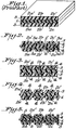
- The invention will now be particularly described, by way of example, with reference to the accompanying drawings in which:-
- Figure 1 is a schematic view, partly in cross-section, of a conventional strip line cable, and
- Figures 2-5 are cross-sectional views of various embodiments of strip line cables according to this invention.
- In the conventional strip line cable of Figure 1 a plurality of pairs of
conductors dielectric material 1 is interposed between the pairs of conductors. A covering orjacket 3 holds the parts of the cable together. The covering is formed by integral moulding, fusion bonding, or adhesion of tape or tapes of PTFE, PFA, FEP, ETFE, or polyester. - The strip line of the present invention is characterised in that an insulation layer of a porous plastic material, preferably expanded, porous PTFE, is interposed between at least one conductor and the covering. The plastic material for the insulation layer should preferably be a fluoroplastic which is superior in electrical and thermal properties to other materials.
- In the strip line cable in accordance with the invention shown in Figure 2, the porous strip or belt-like
dielectric material 1 is expanded, porous PTFE tape having a specific gravity of 0.68 and a thickness of 0.24 mm, produced by known methods. On both sides of thisdielectric material 1 are arranged three sets of pairedconductors conductors conductors 2a',2b' and 2c' is a silver-plated copper wire having a rectangular cross-section, 0.8 mm wide and 0.1 mm thick. Between the silver-plated rectangular copper wires and thecovering 3 is interposed in the longitudinal direction aninsulation layer 4 which is expanded, porous PTFE tape having a specific gravity of 0.68 and a thickness of 0.127 mm. For the sake of convenience, there is shown three sets of conductors in this embodiment. As many sets of conductors as required may be selected. - The assembly of the expanded,
porous PTFE tape 1 and the conductors arranged on both sides thereof is covered entirely with a covering which is a laminate composed of an unsintered, unstretched and unexpanded PTFE layer 3 (0.127 mm thick) and an unsintered expanded, porous PTFE layer 4 (0.127 mm thick and 0.68 in specific gravity). The former layer is placed outside. The assembly thus produced is passed through calender rolls (not shown) and then through a heating bath for 30 minutes, so that the unsintered PTFE layers (one expanded and the other unstretched) are sintered. Thus there is obtained an integral, fusion bonded body composed of theexternal covering 3, theinsulation layer 4, and the expanded, porous PTFEdielectric tape 1. The expanded, porous PTFE tape may be incompletely or partially sintered, and the cable is still useful. - The strip line cable as described above can have the following dimensions and properties. The
porous PTFE tape 1 is 0.17 mm thick. The distance between adjacent conductors is 1.27 mm. The characteristic impedance is 50 ohms. The propagation delay time is 3.7 ns/m, which is comparable to 3.9 ns/m in the case of a conventional strip line cable (as shown in Figure 1) in which the individual conductors are directly covered with the covering 3 made of solid, nonporous insulation material. In addition, the strip line is superior to conventional ones in faithful pulse transmission characteristics and decreased crosstalk between adjacent conductors and between adjacent layers. - In the case of the embodiment shown in Figure 2, compression is accomplished by using a pressure roll system having projecting parts which press only the part held between adjacent conductors. Pressing with such a roll forms grooves 3a in the outer covering, and, as a result, the
dielectric material 1 and theinsulation layer 4 are compressed as indicated by reference numerals 1' and 4'. The configuration in this emodiment is effective in decreasing crosstalk between lines or between layers for the reasons mentioned below. The compressed parts 1' and 4' decrease in porosity and increase in dielectric constant as compared with the other parts of thedielectric material 1 andinsulation layer 4 which remain uncompressed. Each conductor (2a,2a'; 2b,2b'; and 2c,2c') is surrounded by the compressed parts 1' and 41 (having an increased dielectric constant) and the outer covering 3 (having originally a high dielectric constant). This surrounding material absorbs electromagnetic waves, reducing their diffusion. In addition, the grooves formed as mentioned above prevent the strip line from being deformed by force applied in the thickness direction and prevent the conductors from moving in the transverse or widthwise direction. - Figures 3 and 5 show other embodiments of the present invention. In the embodiment shown in Figure 3, each conductor (2a,2a.'; 2b,2b'; and 2c,2c') is first covered entirely with an
insulation layer 4 made of a porous plastic material. The covered conductors are arranged on both sides of the porous strip or belt-likedielectric material 1, and theouter covering 3, made of a nonporous plastic material, is placed on the encased conductors. In the embodiment shown in Figure 4, theinsulation layer 4 of porous plastic material is arranged on one side of each conductor (2a,2a'; 2b,2b'; and 2c,2c') opposite to the porous strip or belt-likedielectric material 1. In both embodiments as shown in Figure 3 and Figure 4, it is permissible to arrange theinsulation layer 4 on only one of the paired signal conductors (e.g. 2a,2b and 2c). It will be easily understood that the embodiments of these structures also produce improved transmission characteristics. - In the embodiment shown in Figure 5, a thin insulation layer 5, which is a nonporous plastic tape such as unstretched PTFE tape, is provided between the porous or belt-like
dielectric material 1 and the paired conductors (2a,2a'; 2b,lb'; and 2c,2c'). This insulation layer increases the dielectric strength of the strip line with a minimum effect on propagation delay time. This insulation layer 5 may be formed on only one side of the belt-likedielectric material 1. In any one of the above-mentioned embodiments, the porous strip or belt-like dielectric material I and/or theinsulation layer 4 of porous plastic material may be made of the porous plastics film having a large number of through holes which is produced according to the process disclosed in Japanese Patent Laid-Open No. 176132/1982 "Sheetlike Resin Material°. The conductors used in the strip line of this device are not limited to those mentioned above. They may be solid wires having a round cross-section or twisted or multiple lines, and they may be copper wire, silver-plated wire, copper-clad steel wire, or gold-plated stainless steel wire, for example. - By means of the embodiments described above, electromagnetic waves in the dielectric material surrounding the signal wires can be absorbed, and propagation delay time reduced.
- In the preferred embodiments the strip or belt-like material made of porous crystalline polymeric material is covered by a material having a higher dielectric constant than said dielectric material. This structure causes the electric field to concentrate within the covering and prevents the electric field of each conductor from radiating outside. This reduces the interlayer crosstalk and interline crosstalk which may take place when the strip lines are placed on top of each other. In addition to the above-mentioned advantages, the strip line cable of this invention may have another advantage, if the resin covering can be easily removed by cutting with a knife, namely that it is easy to handle for terminal formation.
- If necessary, the strip line may be entirely covered with a
shielding layer 6 made, e.g. of metal or conductive fluoroplastic as shown in Figure 3. In the case in which the shielding layer is so close to the conductors that the transmission characteristic may be adversely affected, it will be necessary to make the covering thicker or to interpose a layer of porous crystalline polymeric material, e.g. expanded, porous PTFE, between at least one side of the covering and the shielding layer. In the latter case, it is easy to remove the shielding layer from the main body. - The shape and combination of the conductors are not limited to the embodiments mentioned above. The positions of
conductors conductors conductors 2a',2b' and 2c', so that interlayer crosstalk is reduced. - In the case where the strip line is used in the form of a flat cable, the terminals may be separated from one another or the paired lines at intermediate locations may be separated from one another so as to reduce crosstalk and improve flexibility.
Claims (4)
Applications Claiming Priority (2)
| Application Number | Priority Date | Filing Date | Title |
|---|---|---|---|
| JP1984058184U JPS60169904U (en) | 1984-04-20 | 1984-04-20 | stripline cable |
| JP58184/84 | 1984-04-20 |
Publications (3)
| Publication Number | Publication Date |
|---|---|
| EP0159182A2 true EP0159182A2 (en) | 1985-10-23 |
| EP0159182A3 EP0159182A3 (en) | 1987-01-21 |
| EP0159182B1 EP0159182B1 (en) | 1989-10-11 |
Family
ID=13076926
Family Applications (1)
| Application Number | Title | Priority Date | Filing Date |
|---|---|---|---|
| EP85302554A Expired EP0159182B1 (en) | 1984-04-20 | 1985-04-11 | A strip line cable |
Country Status (6)
| Country | Link |
|---|---|
| US (1) | US4639693A (en) |
| EP (1) | EP0159182B1 (en) |
| JP (1) | JPS60169904U (en) |
| DE (1) | DE3573677D1 (en) |
| HK (1) | HK100991A (en) |
| SG (1) | SG93091G (en) |
Cited By (4)
| Publication number | Priority date | Publication date | Assignee | Title |
|---|---|---|---|---|
| GB2197744A (en) * | 1986-11-19 | 1988-05-25 | Junkosha Co Ltd | An insulated conductor comprising a polytetrafluoroethylene coating |
| EP0310957A2 (en) * | 1987-10-09 | 1989-04-12 | Junkosha Co. Ltd. | Flat cable and method of producing it |
| WO1990001222A1 (en) * | 1988-07-21 | 1990-02-08 | Hughes Aircraft Company | Flexible coaxial cable and method for manufacturing the same |
| EP0402050A2 (en) * | 1989-06-05 | 1990-12-12 | Gec-Marconi Limited | Triplate centre conductors |
Families Citing this family (29)
| Publication number | Priority date | Publication date | Assignee | Title |
|---|---|---|---|---|
| JPH0246061Y2 (en) * | 1986-03-17 | 1990-12-05 | ||
| US5136123A (en) * | 1987-07-17 | 1992-08-04 | Junkosha Co., Ltd. | Multilayer circuit board |
| JPH01129769U (en) * | 1988-02-26 | 1989-09-04 | ||
| US4924037A (en) * | 1988-12-20 | 1990-05-08 | W. L. Gore & Associates, Inc. | Electrical cable |
| JPH02214202A (en) * | 1989-02-14 | 1990-08-27 | Junkosha Co Ltd | Strip line cable |
| US4978813A (en) * | 1989-08-29 | 1990-12-18 | W. L. Gore & Associates, Inc. | Electrical cable |
| US4988835A (en) * | 1989-10-16 | 1991-01-29 | W. L. Gore & Associates, Inc. | Polyvinylidene fluoride electrical cable |
| US5083238A (en) * | 1991-02-04 | 1992-01-21 | Motorola, Inc. | High frequency electronic assembly |
| US5276759A (en) * | 1992-01-09 | 1994-01-04 | Raychem Corporation | Flat cable |
| US5235132A (en) * | 1992-01-29 | 1993-08-10 | W. L. Gore & Associates, Inc. | Externally and internally shielded double-layered flat cable assembly |
| US5502287A (en) * | 1993-03-10 | 1996-03-26 | Raychem Corporation | Multi-component cable assembly |
| US5383788A (en) * | 1993-05-20 | 1995-01-24 | W. L. Gore & Associates, Inc. | Electrical interconnect assembly |
| US5496970A (en) * | 1993-05-20 | 1996-03-05 | W. L. Gore & Associates, Inc. | Planar cable array |
| GB2280547B (en) * | 1993-07-02 | 1997-04-16 | Quantel Ltd | Printed circuit board with integral strip-line structure |
| US5418504A (en) * | 1993-12-09 | 1995-05-23 | Nottenburg; Richard N. | Transmission line |
| US6093886A (en) | 1997-10-28 | 2000-07-25 | University Of Rochester | Vacuum-tight continuous cable feedthrough device |
| US6281451B1 (en) * | 1998-09-24 | 2001-08-28 | International Business Machines Corporation | Electrical cable device |
| US6296725B1 (en) | 1998-09-29 | 2001-10-02 | Litton Systems, Inc. | High frequency ribbon cable for twist capsule cable applications |
| DE10331710B4 (en) * | 2003-07-11 | 2008-05-08 | W. L. Gore & Associates Gmbh | cable |
| US20110120748A1 (en) * | 2006-01-17 | 2011-05-26 | Beru F1 Systems Limited | Wiring component |
| US7659790B2 (en) * | 2006-08-22 | 2010-02-09 | Lecroy Corporation | High speed signal transmission line having reduced thickness regions |
| US20080309349A1 (en) * | 2007-06-15 | 2008-12-18 | Computer Access Technology Corporation | Flexible interposer system |
| US8168891B1 (en) * | 2007-10-26 | 2012-05-01 | Force10 Networks, Inc. | Differential trace profile for printed circuit boards |
| JP4803838B2 (en) * | 2008-02-06 | 2011-10-26 | 清二 加川 | Band-shaped high-frequency transmission line and parallel-type high-frequency transmission line |
| JP5945415B2 (en) * | 2008-09-26 | 2016-07-05 | ナイキ イノベイト シーブイ | Stockfit assembly fixture for shoe manufacturing |
| WO2021025025A1 (en) * | 2019-08-08 | 2021-02-11 | 株式会社村田製作所 | Resin multilayer substrate and method for producing resin multilayer substrate |
| WO2021025024A1 (en) * | 2019-08-08 | 2021-02-11 | 株式会社村田製作所 | Multilayer board and method for manufacturing multilayer board |
| CN111653384A (en) * | 2020-06-22 | 2020-09-11 | 东莞市晟合科技有限公司 | High-speed transmission FFC |
| CN217562291U (en) * | 2021-04-21 | 2022-10-11 | 凡甲电子(苏州)有限公司 | Data transmission cable |
Citations (2)
| Publication number | Priority date | Publication date | Assignee | Title |
|---|---|---|---|---|
| EP0040067A1 (en) * | 1980-05-12 | 1981-11-18 | Junkosha Co. Ltd. | Strip line cable |
| DE3433834A1 (en) * | 1983-09-14 | 1985-03-28 | Junkosha Co. Ltd., Tokio/Tokyo | Highly flexible ribbon cable |
Family Cites Families (7)
| Publication number | Priority date | Publication date | Assignee | Title |
|---|---|---|---|---|
| US3004229A (en) * | 1959-02-24 | 1961-10-10 | Sanders Associates Inc | High frequency transmission line |
| US2994050A (en) * | 1959-04-10 | 1961-07-25 | Sanders Associates Inc | High frequency transmission line |
| JPS5413981A (en) * | 1977-07-01 | 1979-02-01 | Toshiba Corp | Micro strip line |
| JPS5550701A (en) * | 1978-10-06 | 1980-04-12 | Mitsubishi Electric Corp | Microstrip line |
| DE3020622C2 (en) * | 1980-05-30 | 1985-05-15 | W.L. Gore & Associates, Inc., Newark, Del. | Ribbon cable and process for its manufacture |
| JPS57143901A (en) * | 1981-02-27 | 1982-09-06 | Junkosha Co Ltd | Strip line |
| US4490690A (en) * | 1982-04-22 | 1984-12-25 | Junkosha Company, Ltd. | Strip line cable |
-
1984
- 1984-04-20 JP JP1984058184U patent/JPS60169904U/en active Granted
-
1985
- 1985-04-11 EP EP85302554A patent/EP0159182B1/en not_active Expired
- 1985-04-11 DE DE8585302554T patent/DE3573677D1/en not_active Expired
- 1985-04-15 US US06/723,540 patent/US4639693A/en not_active Expired - Lifetime
-
1991
- 1991-11-07 SG SG930/91A patent/SG93091G/en unknown
- 1991-12-12 HK HK1009/91A patent/HK100991A/en not_active IP Right Cessation
Patent Citations (2)
| Publication number | Priority date | Publication date | Assignee | Title |
|---|---|---|---|---|
| EP0040067A1 (en) * | 1980-05-12 | 1981-11-18 | Junkosha Co. Ltd. | Strip line cable |
| DE3433834A1 (en) * | 1983-09-14 | 1985-03-28 | Junkosha Co. Ltd., Tokio/Tokyo | Highly flexible ribbon cable |
Cited By (7)
| Publication number | Priority date | Publication date | Assignee | Title |
|---|---|---|---|---|
| GB2197744A (en) * | 1986-11-19 | 1988-05-25 | Junkosha Co Ltd | An insulated conductor comprising a polytetrafluoroethylene coating |
| EP0310957A2 (en) * | 1987-10-09 | 1989-04-12 | Junkosha Co. Ltd. | Flat cable and method of producing it |
| EP0310957A3 (en) * | 1987-10-09 | 1989-07-26 | Junkosha Co. Ltd. | Flat cable and method of producing it |
| WO1990001222A1 (en) * | 1988-07-21 | 1990-02-08 | Hughes Aircraft Company | Flexible coaxial cable and method for manufacturing the same |
| EP0402050A2 (en) * | 1989-06-05 | 1990-12-12 | Gec-Marconi Limited | Triplate centre conductors |
| EP0402050A3 (en) * | 1989-06-05 | 1991-12-11 | Gec-Marconi Limited | Triplate centre conductors |
| GB2232824B (en) * | 1989-06-05 | 1994-03-02 | Marconi Co Ltd | Triplate waveguide structure |
Also Published As
| Publication number | Publication date |
|---|---|
| EP0159182B1 (en) | 1989-10-11 |
| SG93091G (en) | 1991-12-13 |
| HK100991A (en) | 1991-12-20 |
| US4639693A (en) | 1987-01-27 |
| JPS60169904U (en) | 1985-11-11 |
| JPH0247607Y2 (en) | 1990-12-14 |
| EP0159182A3 (en) | 1987-01-21 |
| DE3573677D1 (en) | 1989-11-16 |
Similar Documents
| Publication | Publication Date | Title |
|---|---|---|
| EP0159182B1 (en) | A strip line cable | |
| EP0040067B1 (en) | Strip line cable | |
| US4423282A (en) | Flat cable | |
| US5235132A (en) | Externally and internally shielded double-layered flat cable assembly | |
| US5025115A (en) | Insulated power cables | |
| US4649228A (en) | Transmission line | |
| US4490690A (en) | Strip line cable | |
| EP0161065B1 (en) | Electrical transmission line | |
| CA1174308A (en) | Flat electric signal cables with a connecting web | |
| GB2058439A (en) | Shielded fiat cable | |
| WO1991014269A1 (en) | Conductively-jacketed electrical cable | |
| US4642480A (en) | Low profile cable with high performance characteristics | |
| US5227742A (en) | Stripline cable having a porous dielectric tape with openings disposed therethrough | |
| US5262589A (en) | High velocity propagation ribbon cable | |
| US20040011552A1 (en) | Controlled impedance extruded flat ribbon cable | |
| FI76449C (en) | band Management | |
| US5744756A (en) | Blown microfiber insulated cable | |
| EP0961298B1 (en) | Electrical signal bundle | |
| CA1255767A (en) | High frequency attenuation cable and harness | |
| US5481069A (en) | Ribbon cable with terminal edge reinforcement | |
| JP3677157B2 (en) | Electrical signal cable assembly | |
| WO1986005311A1 (en) | High performance flat cable | |
| US4300017A (en) | Shielded ribbon cable | |
| JPS6216565B2 (en) | ||
| US4923410A (en) | Low-permittivity connector and flat-cable |
Legal Events
| Date | Code | Title | Description |
|---|---|---|---|
| PUAI | Public reference made under article 153(3) epc to a published international application that has entered the european phase |
Free format text: ORIGINAL CODE: 0009012 |
|
| AK | Designated contracting states |
Designated state(s): DE FR GB |
|
| RAP1 | Party data changed (applicant data changed or rights of an application transferred) |
Owner name: JUNKOSHA CO. LTD. |
|
| PUAL | Search report despatched |
Free format text: ORIGINAL CODE: 0009013 |
|
| AK | Designated contracting states |
Kind code of ref document: A3 Designated state(s): DE FR GB |
|
| 17P | Request for examination filed |
Effective date: 19870623 |
|
| 17Q | First examination report despatched |
Effective date: 19881121 |
|
| GRAA | (expected) grant |
Free format text: ORIGINAL CODE: 0009210 |
|
| AK | Designated contracting states |
Kind code of ref document: B1 Designated state(s): DE FR GB |
|
| REF | Corresponds to: |
Ref document number: 3573677 Country of ref document: DE Date of ref document: 19891116 |
|
| ET | Fr: translation filed | ||
| PLBE | No opposition filed within time limit |
Free format text: ORIGINAL CODE: 0009261 |
|
| STAA | Information on the status of an ep patent application or granted ep patent |
Free format text: STATUS: NO OPPOSITION FILED WITHIN TIME LIMIT |
|
| 26N | No opposition filed | ||
| PGFP | Annual fee paid to national office [announced via postgrant information from national office to epo] |
Ref country code: FR Payment date: 20010319 Year of fee payment: 17 |
|
| PGFP | Annual fee paid to national office [announced via postgrant information from national office to epo] |
Ref country code: DE Payment date: 20010320 Year of fee payment: 17 |
|
| PGFP | Annual fee paid to national office [announced via postgrant information from national office to epo] |
Ref country code: GB Payment date: 20010321 Year of fee payment: 17 |
|
| REG | Reference to a national code |
Ref country code: GB Ref legal event code: IF02 |
|
| PG25 | Lapsed in a contracting state [announced via postgrant information from national office to epo] |
Ref country code: GB Free format text: LAPSE BECAUSE OF NON-PAYMENT OF DUE FEES Effective date: 20020411 |
|
| PG25 | Lapsed in a contracting state [announced via postgrant information from national office to epo] |
Ref country code: DE Free format text: LAPSE BECAUSE OF NON-PAYMENT OF DUE FEES Effective date: 20021101 |
|
| GBPC | Gb: european patent ceased through non-payment of renewal fee |
Effective date: 20020411 |
|
| PG25 | Lapsed in a contracting state [announced via postgrant information from national office to epo] |
Ref country code: FR Free format text: LAPSE BECAUSE OF NON-PAYMENT OF DUE FEES Effective date: 20021231 |
|
| REG | Reference to a national code |
Ref country code: FR Ref legal event code: ST |