EP0157110B1 - Schaltung zur Übertragung eines Binärsignales - Google Patents
Schaltung zur Übertragung eines Binärsignales Download PDFInfo
- Publication number
- EP0157110B1 EP0157110B1 EP85101104A EP85101104A EP0157110B1 EP 0157110 B1 EP0157110 B1 EP 0157110B1 EP 85101104 A EP85101104 A EP 85101104A EP 85101104 A EP85101104 A EP 85101104A EP 0157110 B1 EP0157110 B1 EP 0157110B1
- Authority
- EP
- European Patent Office
- Prior art keywords
- phototransistor
- output
- terminal
- voltage
- emitter
- Prior art date
- Legal status (The legal status is an assumption and is not a legal conclusion. Google has not performed a legal analysis and makes no representation as to the accuracy of the status listed.)
- Expired
Links
Images
Classifications
-
- G—PHYSICS
- G01—MEASURING; TESTING
- G01R—MEASURING ELECTRIC VARIABLES; MEASURING MAGNETIC VARIABLES
- G01R19/00—Arrangements for measuring currents or voltages or for indicating presence or sign thereof
- G01R19/145—Indicating the presence of current or voltage
Definitions
- the present invention relates to a circuit for transmitting a binary signal according to the preamble of the independent claim.
- Such a circuit has become known from US-A-4 197471.
- a phototransistor is provided, the base and emitter of which are directly connected via a parallel connection of a capacitor and a resistor. Emitter and collector form a two-pole with the RC element, which in turn is connected to an evaluation circuit.
- controllable transistor The circuitry of a controllable transistor is known from the article by VP D'YAKONOV “Amplitude limiters and threshold devices based on integrated microcircuits " , published in INSTRUMENTS AND EXPERIMENTAL TECHHIQUES 19 (1976), 3/4, pages 393-396 Base with an input resistor, the emitter with a ground resistance and the collector with the emitter via this chain connection and two inverting voltage-limiting amplifiers and a resistor are connected. The output is taken behind the second amplifier.
- Circuits according to the preamble of claim 1 are used in particular when there is to be galvanic separation between an output pulse voltage with pulses of both polarities and a voltage derived therefrom.
- the field of application of the circuit according to the invention is the derivation of a DC output voltage from an AC mains voltage of in particular 220 V and 50 Hz.
- the task here is to allow the DC output voltage to be present when the input voltage is present, even while keeping a very large voltage tolerance threshold open, the circuit used being said to have Schmitt trigger behavior.
- the solution to this problem consists in the features of the main claim.
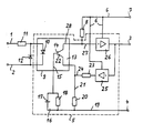
- the drawing shows an electrical circuit.
- the circuit is constructed in the manner of a four-pole circuit and has an input 1 and 2, to which a mains alternating voltage of 50 Hz is preferably connected.
- the four-pole output terminals 3 and 4 also have to be galvanically separated from the input terminals.
- the four-pole is designated 5. It is supplied with a supply operating voltage via a line 6 with a terminal 7 with the interposition of a supply voltage resistor 8.
- Line 6 sets branches for the voltage supply of amplifier stages.
- the main element of the four-pole system is an optocoupler 9, the primary component of which is a light-emitting diode 10, which is connected with its two poles to the two terminals 1 and 2 with the interposition of a resistor 11.
- Parallel to the diode 10 is another diode 12 connected in anti-parallel to it to suppress voltage pulses of the other polarity.
- the opto-coupler On the secondary side, the opto-coupler consists of a photo transistor 13, the base 14 of which is led out of the housing of the opto-coupler via a line 15 and which is connected to an RC element 16. This consists of the parallel connection of a capacitor 17 with an ohmic resistor 18, which is connected on the side facing away from line 15 to a line 19, which in turn leads to terminal 4.
- a line 21 provided with a resistor 20 branches off from the line 19 and is connected to the emitter 22 of the phototransistor.
- a line 24 provided with a resistor 23 branches off from line 21 between emitter 22 and resistor 20 and is led to terminal 3 via an inverting amplifier stage 25.
- Terminal 3 is also connected in parallel to the path just described via an inverting further amplifier stage 26 to a line 27, which in turn leads directly to collector 28 of phototransistor 13.
- the load resistor 8 is connected to the line 27.
- the output voltage goes out when the base voltage of the phototransistor is lowered to such an extent that the capacitor 17 returns to the blocking state again as a result of the capacitor 17 being discharged via the parallel resistor 18.
- the positive feedback effect of switching off the transistor 13 is provided via the load resistor 8 in connection with the two amplifier stages 25 and 26 even when blocking.
- the circuit according to the invention could be varied so that the capacitor 17 can also be placed between the collector and the base of the phototransistor 13.
- the two amplifier stages 25 and 26 can be designed as individual transistors as well as operational amplifiers. If you want to have an output voltage signal at terminals 3 and 4 that becomes zero when there is a pulse train at inputs 1 and 2, you would put output terminal 3 at the output of amplifier stage 25. This enables the logic signal to be inverted.
Landscapes
- Physics & Mathematics (AREA)
- General Physics & Mathematics (AREA)
- Amplifiers (AREA)
- Dc Digital Transmission (AREA)
- Networks Using Active Elements (AREA)
- Communication Control (AREA)
- Electronic Switches (AREA)
Description
- Die vorliegende Erfindung bezieht sich auf eine Schaltung zur Übertragung eines Binärsignales gemäß dem Oberbegriff des unabhängigen Anspruchs.
- Eine solche Schaltung ist bekanntgeworden aus der US-A-4 197471. Hier ist ein Fototransistor vorgesehen, dessen Basis und Emitter über eine Parallelschaltung eines Kondensators und eines Widerstandes unmittelbar verbunden sind. Emitter und Kollektor bilden mit dem RC-Glied einen Zweipol, der mit einer Auswerterschaltung seinerseits verbunden ist.
- Aus dem Aufsatz von V.P. D'YAKONOV « Amplitude limiters and threshold devices based on integrated microcircuits ", erschienen in INSTRUMENTS AND EXPERIMENTAL TECHHIQUES 19 (1976), 3/4, Seiten 393-396, ist die Beschaltung eines steuerbaren Transistors bekannt, wobei die Basis mit einem Eingangswiderstand, der Emitter mit einem Massewiderstand und der Kollektor mit dem Emitter über diese Kettenschaltung und zwei invertierende spannungsbegrenzende Verstärker und einen Widerstand verbunden sind. Der Ausgang ist hinter dem zweiten Verstärker abgenommen.
- Aus der DE-A-2 061 588 ist eine Opto-Koppler-Schaltung bekanntgeworden, bei der ein Fototransistor Verwendung findet, der mit einer der Versorgungsspannungen über einen Widerstand mit dem anderen Pol der Versorgungsspannung hingegen unmittelbar verbunden ist. Von der Basis zum Kollektor ist ein Kondensator geschaltet.
- Schaltungen gemäß dem Oberbegriff des Anspruchs 1, finden insbesondere dann Verwendung, wenn eine galvanische Trennung zwischen einer Ausgangsimpulsspannung mit Impulsen beiderlei Polarität und einer davon abgeleiteten Spannung bestehen soll. Insbesondere ist das Anwendungsgebiet der erfindungsgemäßen Schaltung die Ableitung einer Gleichausgangsspannung von einer Netzwechselspannung von insbesondere 220 V und 50 Hz.
- Hierbei besteht die Aufgabe, die Gleichausgangsspannung dann anstehen zu lassen, wenn die Eingangsspannung anliegt, und zwar auch unter Offenhaltung einer sehr großen Spannungstoleranzschwelle, wobei die verwendete Schaltung Schmitt-Trigger-Verhalten aufweisen soll. Die Lösung dieser Aufgabe besteht in den Merkmalen des Hauptanspruchs.
- Weitere Ausgestaltungen und besonders vorteilhafte Weiterbildungen der Erfindung sind Gegenstand des Unteranspruchs beziehungsweise gehen aus der nachfolgenden Beschreibung hervor, die ein Ausführungsbeispiel der Erfindung anhand der Figur der Zeichnung näher erläutert.
- Die Zeichnung stellt eine elektrische Schaltung dar. Die Schaltung ist nach Art eines Vierpols aufgebaut und weist einen Eingang 1 sowie 2 auf, an denen vorzugsweise eine Netzwechselspannung von 50 Hz anschließt. Weiterhin besitzt der Vierpol Ausgangsklemmen 3 und 4, die von den Eingangsklemmen galvanisch getrennt werden sollen. Der Vierpol ist mit 5 bezeichnet. Er wird über eine Leitung 6 mit einer Klemme 7 unter Zwischenschaltung eines Speisespannungswiderstandes 8 mit einer speisenden Betriebsspannung versorgt. Die Leitung 6 setzt Verzweigungen zur Spannungsversorgung von Verstärkerstufen. Hauptelement des Vierpols ist ein Opto-Koppier 9, dessen primäres Bauteil eine Leuchtdiode 10 ist, die mit ihren beiden Polen unter Zwischenschaltung eines Widerstandes 11 an die beiden Klemmen 1 und 2 angeschlossen ist. Parallel zu der Diode 10 liegt eine weitere zu ihr antiparallel geschaltete Diode 12 zum Unterdrücken von Spannungsimpulsen der anderen Polarität.
- Sekundärseitig besteht der Opto-Koppler aus einem Fototransistor 13, dessen Basis 14 über eine Leitung 15 aus dem Gehäuse des OptoKopplers herausgeführt ist und die mit einem RC-Glied 16 beschaltet ist. Dieses besteht aus der Parallelschaltung eines Kondensators 17 mit einem ohmschen Widerstand 18, die auf der der Leitung 15 abgewandten Seite mit einer Leitung 19 verbunden ist, die ihrerseits zur Klemme 4 führt. Von der Leitung 19 zweigt eine mit einem Widerstand 20 versehene Leitung 21 ab, die mit dem Emitter 22 des Fototransistors verbunden ist.
- Von der Leitung 21 zweigt zwischen dem Emitter 22 und dem Widerstand 20 eine mit einem Widerstand 23 versehene Leitung 24 ab, die über eine invertierende Verstärkerstufe 25 zur Klemme 3 geführt ist. Die Klemme 3 ist andererseits parallel zu dem eben beschriebenen Weg gleichfalls über eine invertierende weitere Verstärkerstufe 26 mit einer Leitung 27 verbunden, die ihrerseits unmittelbar zum Kollektor 28 des Fototransistors 13 führt. An die Leitung 27 ist der Arbeitswiderstand 8 angeschlossen.
- Die Funktion der eben beschriebenen Schaltung ist folgende :
- Betriebsgleichspannung liegt zwischen den Klemmen 7 und 4, an den Eingangsklemmen 1 und 2 liegt keine Impulsspannung an. Damit ist die Leuchtdiode 10 dunkel, der Fototransistor 13 gesperrt. Der Kondensator 17 ist entladen, und zwar über den Widerstand 18. Zwischen den Klemmen 3 und 4 ist keine Spannung, da über den Arbeitswiderstand 8 kein Strom fließt und die beiden Verstärkerstufen 25 und 26 invertieren. Damit liegt am Ausgang des Verstärkers 25 ein Spannungssignal gegenüber der Klemme 4, so daß der Emitter 22 des Fototransistors 13 auf einem Spannungsniveau positiv gegenüber dem der Basis 14 liegt.
- Wird nunmehr an die Klemmen 1 und 2 eine entweder sinusförmige oder rechteckförmige Impulsspannung gelegt, so werden die Impulse der einen Polarität durch die Diode 14 von der Leuchtdiode 10 ferngehalten, während die Leuchtdiode gemäß der Impulsfolge der Impulse der anderen Polarität leuchtet. Dieses Leuchten wird innerhalb des Opto-Koppiers 9 auf den Fototransistor 13 übertragen, so daß die Kollektorbasisstrecke des Fototransistors in der Folge dieser Lichtimpulse leitend wird. Dies führt zu einem Ladestrom für den Kondensator 17. Damit stellt sich auf der Leitung 15, das heißt an der Basis des Fototransistors, ein mittlerer Spannungswert ein, der dem zeitlichen Mittelwert des Fotostroms entspricht. Übersteigt dieser mittlere Spannungswert den Spannungswert, der am Emitter 22 des Fototransistors ansteht, um eine Diodenflußspannung, so wird der Fototransistor leitend, wodurch der Kollektorstrom erheblich ansteigt. Damit entsteht an dem Arbeitswiderstand 8 ein Spannungsabfall, der über die beiden Verstärkerstufen 25 und 26 mit gleichem Vorzeichen auf den Spannungsteiler, bestehend aus den Widerständen 23 und 20, übertragen wird und damit als Mitkopplung auf den Fototransistor 13 wirkt. Damit wird das Kippen des Fototransistors beschleunigt. Dieses Kippen des Fototransistors führt aber zu einem entsprechenden Spannungssignal auf der Klemme 3, so daß zwischen Klemmen 3 und 4 nunmehr eine Ausgangsspannung anliegt. Diese Ausgangsspannung bleibt so lange bestehen, wie über die Fotodiode 10 Impulse übertragen werden. Die Ausgangsspannung erlischt, wenn infolge der Entladung des Kondensators 17 über den Parallelwiderstand 18 die Basisspannung des Fototransistors so weit abgesenkt wird, daß dieser wieder in den Sperrzustand zurückkehrt. Der Mitkoppeleffekt des Abschaltens des Transistors 13 ist über den Arbeitswiderstand 8 in Verbindung mit den beiden Verstärkerstufen 25 und 26 auch beim Sperren gegeben.
- Die erfindungsgemäße Schaltung könnte soweit variiert werden, als daß der Kondensator 17 auch zwischen Kollektor und Basis des Fototransistors 13 gelegt werden kann. Die beiden Verstärkerstufen 25 und 26 können als Einzeltransistoren wie auch als Operationsverstärker ausgebildet sein. Will man ein Ausgangsspannungssignal an den Klemmen 3 und 4 haben, das Null wird, wenn eine Impulsfolge am Eingang 1 und 2 anliegt, würde man die Ausgangsklemme 3 an den Ausgang der Verstärkerstufe 25 legen. Hiermit ist eine Invertierung des logischen Signals möglich.
Claims (2)
Priority Applications (1)
| Application Number | Priority Date | Filing Date | Title |
|---|---|---|---|
| AT85101104T ATE48191T1 (de) | 1984-02-25 | 1985-02-02 | Schaltung zur uebertragung eines binaersignales. |
Applications Claiming Priority (2)
| Application Number | Priority Date | Filing Date | Title |
|---|---|---|---|
| DE8406144U | 1984-02-25 | ||
| DE8406144 | 1984-02-25 |
Publications (2)
| Publication Number | Publication Date |
|---|---|
| EP0157110A1 EP0157110A1 (de) | 1985-10-09 |
| EP0157110B1 true EP0157110B1 (de) | 1989-11-23 |
Family
ID=6764158
Family Applications (1)
| Application Number | Title | Priority Date | Filing Date |
|---|---|---|---|
| EP85101104A Expired EP0157110B1 (de) | 1984-02-25 | 1985-02-02 | Schaltung zur Übertragung eines Binärsignales |
Country Status (3)
| Country | Link |
|---|---|
| EP (1) | EP0157110B1 (de) |
| AT (1) | ATE48191T1 (de) |
| DE (1) | DE3574413D1 (de) |
Family Cites Families (3)
| Publication number | Priority date | Publication date | Assignee | Title |
|---|---|---|---|---|
| DE2061588B1 (de) * | 1970-12-15 | 1972-05-25 | Siemens Ag | Schaltung zur Entzerrung und/oder Konstanthaltung des Tastverhältnisses |
| US4063121A (en) * | 1976-07-22 | 1977-12-13 | Automation Systems Inc. | Input converter |
| US4197471A (en) * | 1977-09-29 | 1980-04-08 | Texas Instruments Incorporated | Circuit for interfacing between an external signal and control apparatus |
-
1985
- 1985-02-02 EP EP85101104A patent/EP0157110B1/de not_active Expired
- 1985-02-02 AT AT85101104T patent/ATE48191T1/de not_active IP Right Cessation
- 1985-02-02 DE DE8585101104T patent/DE3574413D1/de not_active Expired
Also Published As
| Publication number | Publication date |
|---|---|
| DE3574413D1 (en) | 1989-12-28 |
| EP0157110A1 (de) | 1985-10-09 |
| ATE48191T1 (de) | 1989-12-15 |
Similar Documents
| Publication | Publication Date | Title |
|---|---|---|
| DE2649024C3 (de) | Teilnehmerschaltung | |
| DE2727537A1 (de) | Schwellwert-detektor | |
| DE2061943C3 (de) | Differenzverstärker | |
| DE3448118C2 (de) | ||
| EP0292804B1 (de) | Schaltungsanordnung zur potentialfreien Erfassung von binären Signalen | |
| EP0254214B1 (de) | Integrierbare Schaltung zur Pegelumsetzung | |
| DE3503531A1 (de) | Schaltung zur uebertragung eines binaersignales | |
| DE602004000299T2 (de) | Fotoelektrische Strom-/Spannungs-Wandlerschaltung | |
| EP0157110A1 (de) | Schaltung zur Übertragung eines Binärsignales | |
| DE3744079A1 (de) | Anordnung zum umsetzen von einer innerhalb eines grossen bereichs veraenderlichen spannung in ein binaeres informationsmaterial | |
| DE3722336C1 (de) | Elektronisches,vorzugsweise beruehrungslos arbeitendes Schaltgeraet | |
| DE3427862C2 (de) | ||
| EP0048490B1 (de) | Schaltungsanordnung zum Umsetzen eines binären Eingangssignals in ein Telegrafiersignal | |
| DE2721514C2 (de) | Schaltungsanordnung zum Umsetzen eines binären Eingangssignals in ein Telegrafiesignal | |
| DE2748292A1 (de) | Vorrichtung zum uebertragen von signalen | |
| EP1002363B1 (de) | Vorrichtung zum umsetzen kleiner, von einer nicht-idealen stromquelle an dem eingang der vorrichtung eingeprägter ströme in spannungssignale | |
| DE19510387C1 (de) | Polaritätsanzeigeeinrichtung | |
| CH648168A5 (de) | Elektronischer sender fuer gleichstromtelegraphiesysteme. | |
| DE3744756A1 (de) | Konstantstromgenerator | |
| EP0296307A1 (de) | Schaltungsanordnung für einen analogen, elektronischen Regler | |
| DE9112419U1 (de) | Einrichtung zur Folgeumschaltung | |
| EP0299259B1 (de) | Elektronisches, vorzugsweise berührungslos arbeitendes Schaltgerät | |
| DE3913798A1 (de) | Schaltungsanordnung zum potentialfreien ansteuern eines aktors | |
| EP0846284B1 (de) | Anpassschaltung für ein elektronisches bauteil oder eine baugruppe | |
| DE3014214A1 (de) | Anordnung zur uebertragung digitaler signale auf einer uebertragungsstrecke |
Legal Events
| Date | Code | Title | Description |
|---|---|---|---|
| PUAI | Public reference made under article 153(3) epc to a published international application that has entered the european phase |
Free format text: ORIGINAL CODE: 0009012 |
|
| AK | Designated contracting states |
Designated state(s): AT BE CH DE FR GB IT LI LU NL SE |
|
| 17P | Request for examination filed |
Effective date: 19860326 |
|
| 17Q | First examination report despatched |
Effective date: 19880330 |
|
| RAP1 | Party data changed (applicant data changed or rights of an application transferred) |
Owner name: VAILLANT GMBH Owner name: SCHONEWELLE B.V. Owner name: VAILLANT LTD. Owner name: VAILLANT GES.M.B.H Owner name: VAILLANT S.A.R.L Owner name: COFRABEL N.V. Owner name: JOH. VAILLANT GMBH U. CO. |
|
| GRAA | (expected) grant |
Free format text: ORIGINAL CODE: 0009210 |
|
| AK | Designated contracting states |
Kind code of ref document: B1 Designated state(s): AT BE CH DE FR GB IT LI LU NL SE |
|
| REF | Corresponds to: |
Ref document number: 48191 Country of ref document: AT Date of ref document: 19891215 Kind code of ref document: T |
|
| REF | Corresponds to: |
Ref document number: 3574413 Country of ref document: DE Date of ref document: 19891228 |
|
| GBT | Gb: translation of ep patent filed (gb section 77(6)(a)/1977) | ||
| ITF | It: translation for a ep patent filed | ||
| ET | Fr: translation filed | ||
| PLBE | No opposition filed within time limit |
Free format text: ORIGINAL CODE: 0009261 |
|
| STAA | Information on the status of an ep patent application or granted ep patent |
Free format text: STATUS: NO OPPOSITION FILED WITHIN TIME LIMIT |
|
| 26N | No opposition filed | ||
| ITTA | It: last paid annual fee | ||
| PGFP | Annual fee paid to national office [announced via postgrant information from national office to epo] |
Ref country code: SE Payment date: 19921207 Year of fee payment: 9 Ref country code: FR Payment date: 19921207 Year of fee payment: 9 |
|
| PGFP | Annual fee paid to national office [announced via postgrant information from national office to epo] |
Ref country code: LU Payment date: 19921209 Year of fee payment: 9 |
|
| PGFP | Annual fee paid to national office [announced via postgrant information from national office to epo] |
Ref country code: GB Payment date: 19921211 Year of fee payment: 9 |
|
| PGFP | Annual fee paid to national office [announced via postgrant information from national office to epo] |
Ref country code: BE Payment date: 19930114 Year of fee payment: 9 |
|
| PGFP | Annual fee paid to national office [announced via postgrant information from national office to epo] |
Ref country code: NL Payment date: 19930228 Year of fee payment: 9 |
|
| EPTA | Lu: last paid annual fee | ||
| NLT1 | Nl: modifications of names registered in virtue of documents presented to the patent office pursuant to art. 16 a, paragraph 1 |
Owner name: VAILLANT B.V. TE AMSTERDAM. |
|
| PG25 | Lapsed in a contracting state [announced via postgrant information from national office to epo] |
Ref country code: LU Free format text: LAPSE BECAUSE OF NON-PAYMENT OF DUE FEES Effective date: 19940202 Ref country code: GB Effective date: 19940202 |
|
| PG25 | Lapsed in a contracting state [announced via postgrant information from national office to epo] |
Ref country code: SE Effective date: 19940203 |
|
| PG25 | Lapsed in a contracting state [announced via postgrant information from national office to epo] |
Ref country code: BE Effective date: 19940228 |
|
| BERE | Be: lapsed |
Owner name: COFRABEL N.V. Effective date: 19940228 |
|
| PG25 | Lapsed in a contracting state [announced via postgrant information from national office to epo] |
Ref country code: NL Effective date: 19940901 |
|
| GBPC | Gb: european patent ceased through non-payment of renewal fee |
Effective date: 19940202 |
|
| NLV4 | Nl: lapsed or anulled due to non-payment of the annual fee | ||
| PG25 | Lapsed in a contracting state [announced via postgrant information from national office to epo] |
Ref country code: FR Effective date: 19941031 |
|
| REG | Reference to a national code |
Ref country code: FR Ref legal event code: ST |
|
| PGFP | Annual fee paid to national office [announced via postgrant information from national office to epo] |
Ref country code: DE Payment date: 19950101 Year of fee payment: 11 |
|
| PGFP | Annual fee paid to national office [announced via postgrant information from national office to epo] |
Ref country code: AT Payment date: 19950125 Year of fee payment: 11 |
|
| PGFP | Annual fee paid to national office [announced via postgrant information from national office to epo] |
Ref country code: CH Payment date: 19950127 Year of fee payment: 11 |
|
| EUG | Se: european patent has lapsed |
Ref document number: 85101104.9 Effective date: 19940910 |
|
| PG25 | Lapsed in a contracting state [announced via postgrant information from national office to epo] |
Ref country code: AT Effective date: 19960202 |
|
| PG25 | Lapsed in a contracting state [announced via postgrant information from national office to epo] |
Ref country code: LI Free format text: LAPSE BECAUSE OF NON-PAYMENT OF DUE FEES Effective date: 19960228 Ref country code: CH Free format text: LAPSE BECAUSE OF NON-PAYMENT OF DUE FEES Effective date: 19960228 |
|
| REG | Reference to a national code |
Ref country code: CH Ref legal event code: PL |
|
| PG25 | Lapsed in a contracting state [announced via postgrant information from national office to epo] |
Ref country code: DE Effective date: 19961101 |