EP0154725A2 - Méthode et circuit pour démarrer une connexion de transmission de données - Google Patents
Méthode et circuit pour démarrer une connexion de transmission de données Download PDFInfo
- Publication number
- EP0154725A2 EP0154725A2 EP84116479A EP84116479A EP0154725A2 EP 0154725 A2 EP0154725 A2 EP 0154725A2 EP 84116479 A EP84116479 A EP 84116479A EP 84116479 A EP84116479 A EP 84116479A EP 0154725 A2 EP0154725 A2 EP 0154725A2
- Authority
- EP
- European Patent Office
- Prior art keywords
- data processing
- circuit
- ready
- processing unit
- identifier
- Prior art date
- Legal status (The legal status is an assumption and is not a legal conclusion. Google has not performed a legal analysis and makes no representation as to the accuracy of the status listed.)
- Withdrawn
Links
Images
Classifications
-
- G—PHYSICS
- G06—COMPUTING OR CALCULATING; COUNTING
- G06F—ELECTRIC DIGITAL DATA PROCESSING
- G06F13/00—Interconnection of, or transfer of information or other signals between, memories, input/output devices or central processing units
- G06F13/14—Handling requests for interconnection or transfer
- G06F13/36—Handling requests for interconnection or transfer for access to common bus or bus system
- G06F13/368—Handling requests for interconnection or transfer for access to common bus or bus system with decentralised access control
- G06F13/374—Handling requests for interconnection or transfer for access to common bus or bus system with decentralised access control using a self-select method with individual priority code comparator
Definitions
- the invention relates to a method for initiating a data transmission connection between one of a plurality of ready-to-send data processing units and one or more further data processing units to be controlled via a multiple line arrangement, in which a selection start signal on a control line of the multiple line arrangement in a ready-to-send data processing unit causes a priority determination during a selection phase preceding the respective data transmission.
- a data processing system in which a plurality of data processing units can communicate with one another via a multiple line arrangement is also referred to as a multiple processor system.
- multiple processors are connected to one another via the multiple-line arrangement, which is also referred to as a bus, and each form an independent data processing unit with a central unit, main memory, bus coupler and input-output interface.
- An initialization process within the data processing system provides for a distribution of the various data processing tasks to the processors, which is based on aspects such as the necessary degree of parallel data processing or the current load status of individual processors.
- This distribution of work leads to a constantly changing workload in the dynamic state of the data processing system, which in turn must be controlled according to the priorities to be specified.
- the processors are subject to dynamic priority assignment with regard to their access to other processors via the bus. If a processor is to be connected to another processor, it must be checked in the context of such a priority assignment whether another one Processor with higher priority is privileged to access the bus and in turn establish a data transmission connection.
- the priority determination required for this has hitherto been carried out in such a way that of several processors expressing an access request, the one with the highest priority is determined and only then has its data transmission connection been established with another processor.
- this principle is associated with the disadvantage that the priority determination must be repeated if the receiving processor controlled by the processor of the highest priority via the bus is not ready to receive and emits a corresponding status signal which identifies its occupied state.
- the priority determination must also be repeated in the course of new connection attempts until the desired processor identifies its idle state and the desired data transmission connection can be established.
- this involves a time expenditure which depends on the respective dynamic state of the operating sequence of the data processing system and therefore cannot be estimated. If one wants to reduce this expenditure of time, additional lines can be provided within the multiple line arrangement in order to carry out a status determination in parallel with the addressing of a desired processor. However, this is undesirable because it greatly increases the overall circuit complexity for the data processing system.
- the invention is based on the object of specifying a method and a circuit arrangement for initiating a data transmission connection which, even in the case of a processor which is not ready to receive, takes much less time than previously known principles.
- a method of the type mentioned at the outset is designed to achieve this object in such a way that each ready-to-receive data processing unit, on a line of the multiple line arrangement assigned to it at least within the selection phase, emits a reception identifier which identifies its ready-to-receive state, in each ready-to-transmit state, upon receipt of the selection start signal
- a data processing unit is checked to determine whether the reception identifier is present on the line assigned to the data processing unit to be controlled, and if this reception identifier is present on a line of the multiple line arrangement assigned to this data processing unit that is ready for transmission, a transmission identifier is given at least within the selection phase and that the priority determination is only carried out by transmitting identification evaluation is carried out in those ready-to-send data processing units which have
- the method according to the invention therefore provides for a specific assignment of the individual lines of the multiple line arrangement (bus) to the individual data processing units within the selection phase, which precedes the actual data transmission and in which the data transmission connection is set up.
- a distinction can be made between two time intervals during the selection phase, the first of which is provided for issuing the reception identifiers from all data processing units of the system that are ready to receive. The second interval then serves to deliver the transmission identifiers over the permanently assigned lines.
- each ready-to-send data processing unit in the first time interval it is determined in each ready-to-send data processing unit in the first time interval whether the receiving data processing unit desired by it is ready to receive is or not, for which purpose only a comparison of the receive identifiers present on the bus with the receiver address present in the ready-to-send data processing unit is to be carried out.
- This comparison is possible because the fixed assignment provided in the first time interval in each case one line of the multiple line arrangement to a respective data processing unit.
- B. is available in the context of an assignment table, which was created when the system was initialized and can be present in the memory of each data processing unit.
- the priority determination can be carried out decentrally in each of these ready-to-send data processing units by comparing the send identifiers appearing on the bus in a very simple manner a priority table are performed, similar to the mapping table in each data processing unit - is present. If it emerges from this comparison that the respective data processing unit carrying out the comparison has a lower priority than another one, then its switching off is initiated by the multiple line arrangement and the data transmission connection desired by it is re-initiated at a later point in time.
- a significant advantage of a method according to the invention is the possibility of being able to keep pace with the technological development of the multiprocessor systems even as part of the priority determination, because the priority determination is not program-controlled in logical individual steps, but already within the selection phase using circuitry only from processors ready to receive provided signals. Since there is no evaluation in several addressing and verification steps, the priority determination and thus the advantages of fast circuit technology for the selection phase can be fully used and the selection phase can be made as short as possible.
- the data processing units ready to receive first give their receive identifiers to the multiple line
- the comparison of these receive identifiers carried out in the manner described in each sending data processing unit with the respectively desired recipient address achieves an automatic preselection of only those receiving data processing units that are suitable for the Establishing a data transmission connection are of interest at all.
- To determine priority only a single evaluation step is required, because only processors capable of communication are involved and in any case the initiated data transmission connection remains that which is assigned the highest priority. No additional lines of the multi-line system are required to transmit the criteria which control this priority determination, because the normal data transmission lines can be used for this purpose, which only have to be operated in the selection phase in the described fixed assignment to each data processing unit or to each processor.
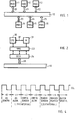
- FIG. 1 shows a data processing system in which a plurality of processors 11 to 16 are connected to a multiple line arrangement 10, hereinafter referred to as bus, as data processing units, each via a bus coupling line arrangement 20 to 25.
- bus multiple line arrangement
- processors 11 to 16 are provided, which can perform matching or different tasks within the framework of the overall system, as is known per se for multiprocessor systems of this type.
- two processors can communicate with each other via the bus 10, for which purpose the respective data transmission connection is preceded by a selection phase. This selection phase is initiated in a manner to be described by a processor expressing a connection request, it being checked whether the desired processor is ready to receive or not.
- the lack of readiness to receive may be due, for example, to a data transmission connection which is still in use and through which the bus 10 is occupied, or internal data processing operations which generate new data can be processed in the desired processor Prevent transmission link. Since the processors 11 to 16 must be used with a variable load distribution with different priorities, a priority determination must also be carried out in addition to an addressing process for the purpose of establishing a connection, as was already generally explained above.
- FIG. 2 shows the most important functional units of a processor connected to the bus 10.
- This contains a central processing unit 30 (CPU), to which a main memory 31 (M) is assigned via an internal connection 32, which contains a main memory controller (not shown).
- the central unit 30 and the main memory 31 are in turn connected to a memory organization unit 33 (MMU), which can also take over main memory control tasks and via which internal data processing within the processor can be carried out.
- MMU memory organization unit 33
- the signals required for this, received via the bus 10, and signals to be output via the bus 10 are controlled by a bus coupling circuit 34 (BCU), which is connected to the bus 10 via a bus coupling line arrangement 35.
- BCU bus coupling circuit 34
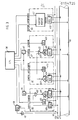
- the bus coupling circuit 34 contains the functional units with which a connection is established between two or more processors during the selection phase and the decentralized priority is determined. These functional units are explained with reference to FIG. 3. 3 shows an arrangement of four individual circuits 40, 41, 42 and 43, which represent the essential functional units for initiating a data transmission connection and are controlled by the central unit 30.
- the circuit 40 is a receive identification transmission circuit and contains, as an essential component, a demultiplexer 401, the input of which is connected to an AND gate 402.
- the demultiplexer 401 can e.g. B. be an integrated circuit of the type 74138. Its selection inputs are controlled by an address register 403.
- the outputs of the demultiplexer 401 are connected to an output register 404, the register outputs of which are each connected to one line of the bus 10.
- a register 405 is also provided, the output of which is connected to an input of the AND gate 402.
- the second input of the AND gate 402 is connected to a ready-to-receive circuit 44 (R) which signals the readiness to receive the processor and is controlled accordingly by the central unit 30.
- the readiness to send is signaled by a readiness to send circuit 45 (T), which is also controlled by the central unit 30.
- the registers 404 and 405 are activated by the central clock CCL of the overall system at different times t1 and t2 and are connected with their control inputs to the central clock line 46 accordingly.
- the register 405 serves to receive a selection start signal AS via a selection start signal line 47 common to all processors.
- the output of a register 48 is connected to this selection start signal line, which receives the selection start signal from the central unit 30, is activated at a time t0 via the central clock line 46 and the selection start signal then via an open collector circuit 49 outputs on the selection start signal line 47.
- the address register 403 is used to hold an address ADI which is assigned to the processor which contains the circuit shown in FIG. 3. It is therefore the internal processor address which is supplied to the address register 403 by the central unit 30 and can also be changed depending on the position of the processor in the system.
- the reception identifier transmission circuit 40 can give a reception identifier to the line of the bus 10 assigned to it as soon as the reception standby circuit 44 signals the readiness for reception of the processor with appropriate control by the central unit 30 and a selection start signal has occurred on the selection start signal line 47 at time t0, which is ready for transmission Processor on the selection start signal line 47 was given.
- This selection start signal is transferred to the register 405, which drives the AND gate 402 at time t1 and outputs a signal indicating readiness for transmission to the demultiplexer 401. This outputs an output at its output addressed by its own processor address ADI
- Receive identifier from a point in the output register 404, the output line of which is connected to a line of the bus 10 which, due to the described function of the demultiplexer 401, is permanently assigned to the circuit shown in FIG. 3 and thus to the corresponding processor.
- the reception identifier is transferred to bus 10 at time t2.
- the circuit 41 is a reception identification recording circuit and contains a multiplexer 411, which e.g. B. can be an integrated circuit of the type 74151 and
- the address register 413 is used to hold the address ADN of a processor with which a data transmission connection is to be established, i. H. that is desired by the processor associated with the circuit of FIG. 3.
- the multiplexer 411 is connected to the outputs of an input register 414, the inputs of which are each connected to one line of the bus 10.
- receive identifiers on the individual lines of the bus 10 are transferred to the input register 414 and transferred to the multiplexer 411 at time t3.
- the receive identifier which comes from the desired processor with the address ADN is generated by the multiplexer 411 as a result of the described
- Circuit 42 which is a transmission identifier transmission circuit.
- This transmit identifier transmit circuit is constructed similarly to the receive identifier transmit circuit 40 and contains an AND gate 422 which is connected to a demultiplexer 421, which may be an integrated circuit of the 74138 type and contains a switching function which is controlled by an address register 423, which takes up the internal processor address ADI of the processor which is assigned to the circuit shown in FIG. 3.
- the demultiplexer 421 is followed by an output register 424, the output lines of which are each connected to one line of the bus 10 and which is activated at time t4.
- the AND gate 422 is the described output signal of the multiplexer 411 Receive identification recording circuit 41 and driven by the ready-to-send signal from the ready-to-send circuit 45.
- the circuit 43 is a transmission identification recording circuit and contains a priority determination circuit 431, which is also referred to as an arbitrator and is driven via an input register 432 at time t5.
- the input register 432 is connected with its input lines to one line of the bus 10 in each case and takes up the transmission identifiers which appear overall on the bus 10.
- these transmission identifiers are issued to the referee 431, who then, under the control of a priority rule which is common to all central units of the data transmission system, determines the priority of the processor assigned to the circuit according to FIG. 3 in order to determine whether this processor is from the bus 10 must switch off due to higher priority of another processor or not, which is then done by the central unit 30.
- FIG. 4 shows the central clock CCL of the data transfer system with the individual cycle intervals t0 to t5.
- the selection start signal AS is passed onto the selection start signal line 47 by a processor which is ready to send and which wishes to connect to another processor.
- This selection start signal is received in the reception identifier transmission circuit 40 of all processors with the register 405 during the clock interval t1 and evaluated in the manner described.
- these receive identifiers are evaluated in the manner described in the processor ready to send in each case in order to determine whether the receive identifier of the desired processor is present. If this is the case, then in the clock interval t4 the transmission identifier is given to that line of the bus 10 which is permanently assigned to the respective processor. Thus, only the send identifiers of those processors that are capable of communication appear on the bus 10, i. H. that have addressed a processor ready to receive.
- transmit identifiers are taken over by the transmit identifier recording circuits 43 of these processors in the clock interval t5, and a priority determination is carried out in each processor, which means that only the processor with the highest priority maintains its connection to the bus 10, while the other processors disconnect from bus 10. The one still connected to bus 10 The processor can then start the actual data transmission with the processor addressed by it via the bus 10.
Landscapes
- Engineering & Computer Science (AREA)
- Theoretical Computer Science (AREA)
- Physics & Mathematics (AREA)
- General Engineering & Computer Science (AREA)
- General Physics & Mathematics (AREA)
- Multi Processors (AREA)
- Bus Control (AREA)
- Computer And Data Communications (AREA)
- Small-Scale Networks (AREA)
- Communication Control (AREA)
Applications Claiming Priority (2)
| Application Number | Priority Date | Filing Date | Title |
|---|---|---|---|
| DE3407870 | 1984-03-02 | ||
| DE19843407870 DE3407870C1 (de) | 1984-03-02 | 1984-03-02 | Verfahren und Schaltungsanordnung zum Einleiten einer Datenuebertragungsverbindung |
Publications (2)
| Publication Number | Publication Date |
|---|---|
| EP0154725A2 true EP0154725A2 (fr) | 1985-09-18 |
| EP0154725A3 EP0154725A3 (fr) | 1987-04-15 |
Family
ID=6229498
Family Applications (1)
| Application Number | Title | Priority Date | Filing Date |
|---|---|---|---|
| EP84116479A Withdrawn EP0154725A3 (fr) | 1984-03-02 | 1984-12-28 | Méthode et circuit pour démarrer une connexion de transmission de données |
Country Status (3)
| Country | Link |
|---|---|
| EP (1) | EP0154725A3 (fr) |
| JP (1) | JPS60205651A (fr) |
| DE (1) | DE3407870C1 (fr) |
Cited By (1)
| Publication number | Priority date | Publication date | Assignee | Title |
|---|---|---|---|---|
| DE3928481A1 (de) * | 1989-08-29 | 1991-03-14 | Diehl Gmbh & Co | Prioritaetsorientiertes busvergabesystem |
Families Citing this family (1)
| Publication number | Priority date | Publication date | Assignee | Title |
|---|---|---|---|---|
| US4858173A (en) * | 1986-01-29 | 1989-08-15 | Digital Equipment Corporation | Apparatus and method for responding to an aborted signal exchange between subsystems in a data processing system |
Family Cites Families (2)
| Publication number | Priority date | Publication date | Assignee | Title |
|---|---|---|---|---|
| US4038644A (en) * | 1975-11-19 | 1977-07-26 | Ncr Corporation | Destination selection apparatus for a bus oriented computer system |
| US4320452A (en) * | 1978-06-29 | 1982-03-16 | Standard Oil Company (Indiana) | Digital bus and control circuitry for data routing and transmission |
-
1984
- 1984-03-02 DE DE19843407870 patent/DE3407870C1/de not_active Expired
- 1984-12-28 EP EP84116479A patent/EP0154725A3/fr not_active Withdrawn
-
1985
- 1985-03-01 JP JP60040956A patent/JPS60205651A/ja active Granted
Cited By (1)
| Publication number | Priority date | Publication date | Assignee | Title |
|---|---|---|---|---|
| DE3928481A1 (de) * | 1989-08-29 | 1991-03-14 | Diehl Gmbh & Co | Prioritaetsorientiertes busvergabesystem |
Also Published As
| Publication number | Publication date |
|---|---|
| JPH0343656B2 (fr) | 1991-07-03 |
| EP0154725A3 (fr) | 1987-04-15 |
| JPS60205651A (ja) | 1985-10-17 |
| DE3407870C1 (de) | 1985-08-14 |
Similar Documents
| Publication | Publication Date | Title |
|---|---|---|
| DE2944497C2 (fr) | ||
| DE3300260C2 (fr) | ||
| DE3300261C2 (fr) | ||
| DE3942661C2 (fr) | ||
| EP0743595B1 (fr) | Système de communication avec des moyens pour l'echange de logiciel | |
| DE1299145B (de) | Schaltungsanordnung zum Steuern von peripheren Ein- und Ausgabegeraeten von Datenverarbeitungssystemen | |
| DE2332734A1 (de) | Datenverarbeitungssystem | |
| DE1424762B2 (de) | Datenverarbeitungsanlage | |
| DE3103786A1 (de) | Datenuebertragungssystem | |
| DE69429325T2 (de) | Datenvermittlungsvorrichtung | |
| EP0185260B1 (fr) | Interface pour le transfert direct d'informations | |
| DE3048414A1 (de) | "schaltungsanordnung fuer eine datenverarbeitungsanlage" | |
| DE60211874T2 (de) | Anordnung von zwei Geräten, verbunden durch einen Kreuzvermittlungsschalter | |
| DE68927157T2 (de) | Deblockierverfahren eines Multiprozessor-Multibus-Systems | |
| DE1524127B2 (de) | Mehrfachrechenanlage mit internen verbindungsleitungen zwischen den datenverarbeitungsgeraeten | |
| EP0154725A2 (fr) | Méthode et circuit pour démarrer une connexion de transmission de données | |
| EP0104638B1 (fr) | Méthode pour la préparation de la connexion d'une ou de plusieurs unités de traitement de données à un système de multiples lignes, commandé par une horloge centrale | |
| DE2507405A1 (de) | Verfahren und anordnung zum synchronisieren der tasks in peripheriegeraeten in einer datenverarbeitungsanlage | |
| DE2612316C3 (de) | Anordnung zur Steuerung des Multiplexbetriebes zwischen mehreren Kanälen und einer zentralen Steuerschaltung eines Ein-/Ausgabewerkes in einem Datenverarbeitungssystem | |
| DE3935707A1 (de) | System zur verbindung von rechnern mit ihrer peripheren ausruestung | |
| DE2606295A1 (de) | Verfahren zum ausfuehren einer datenuebertragung zwischen peripheren einheiten und einem arbeitsspeicher ueber einen multiplexkanal | |
| DE2339813C3 (de) | Verfahren zum Starten von peripheren Geraten an einem Blockmultiplexkanal | |
| DE19756885A1 (de) | Verfahren zum Austausch von Signalen zwischen über einen Bus verbundenen Modulen sowie Vorrichtung zur Durchführung des Verfahrens | |
| DE3716506A1 (de) | System mit zwei mikroprozessoren | |
| DE2452324A1 (de) | Einrichtung fuer den selektiven austausch von informationen |
Legal Events
| Date | Code | Title | Description |
|---|---|---|---|
| PUAI | Public reference made under article 153(3) epc to a published international application that has entered the european phase |
Free format text: ORIGINAL CODE: 0009012 |
|
| AK | Designated contracting states |
Designated state(s): AT BE CH DE FR GB IT LI LU NL SE |
|
| PUAL | Search report despatched |
Free format text: ORIGINAL CODE: 0009013 |
|
| AK | Designated contracting states |
Kind code of ref document: A3 Designated state(s): AT BE CH DE FR GB IT LI LU NL SE |
|
| 17P | Request for examination filed |
Effective date: 19870908 |
|
| RBV | Designated contracting states (corrected) |
Designated state(s): AT CH DE FR GB IT LI NL SE |
|
| 17Q | First examination report despatched |
Effective date: 19880516 |
|
| STAA | Information on the status of an ep patent application or granted ep patent |
Free format text: STATUS: THE APPLICATION HAS BEEN WITHDRAWN |
|
| 18W | Application withdrawn |
Withdrawal date: 19880923 |
|
| RIN1 | Information on inventor provided before grant (corrected) |
Inventor name: UNGER, MANFRED Inventor name: EISENACK, JOACHIM Inventor name: STAEHLE, PETER |