EP0152913A2 - Schaltungsanordnung für ein Sperrwandler-Schaltnetzteil - Google Patents
Schaltungsanordnung für ein Sperrwandler-Schaltnetzteil Download PDFInfo
- Publication number
- EP0152913A2 EP0152913A2 EP85101577A EP85101577A EP0152913A2 EP 0152913 A2 EP0152913 A2 EP 0152913A2 EP 85101577 A EP85101577 A EP 85101577A EP 85101577 A EP85101577 A EP 85101577A EP 0152913 A2 EP0152913 A2 EP 0152913A2
- Authority
- EP
- European Patent Office
- Prior art keywords
- winding
- supply
- circuit
- voltage
- input
- Prior art date
- Legal status (The legal status is an assumption and is not a legal conclusion. Google has not performed a legal analysis and makes no representation as to the accuracy of the status listed.)
- Granted
Links
- 238000004804 winding Methods 0.000 claims abstract description 27
- 230000000903 blocking effect Effects 0.000 claims abstract description 4
- 238000005259 measurement Methods 0.000 claims 2
- 238000012216 screening Methods 0.000 claims 1
- 239000003990 capacitor Substances 0.000 description 8
- 230000010355 oscillation Effects 0.000 description 3
- 230000006378 damage Effects 0.000 description 1
- 238000011161 development Methods 0.000 description 1
- 230000018109 developmental process Effects 0.000 description 1
- 230000001939 inductive effect Effects 0.000 description 1
- 238000002955 isolation Methods 0.000 description 1
- 238000000034 method Methods 0.000 description 1
- 238000012544 monitoring process Methods 0.000 description 1
- 238000005457 optimization Methods 0.000 description 1
Images

Classifications
-
- H—ELECTRICITY
- H02—GENERATION; CONVERSION OR DISTRIBUTION OF ELECTRIC POWER
- H02M—APPARATUS FOR CONVERSION BETWEEN AC AND AC, BETWEEN AC AND DC, OR BETWEEN DC AND DC, AND FOR USE WITH MAINS OR SIMILAR POWER SUPPLY SYSTEMS; CONVERSION OF DC OR AC INPUT POWER INTO SURGE OUTPUT POWER; CONTROL OR REGULATION THEREOF
- H02M1/00—Details of apparatus for conversion
- H02M1/36—Means for starting or stopping converters
-
- H—ELECTRICITY
- H02—GENERATION; CONVERSION OR DISTRIBUTION OF ELECTRIC POWER
- H02M—APPARATUS FOR CONVERSION BETWEEN AC AND AC, BETWEEN AC AND DC, OR BETWEEN DC AND DC, AND FOR USE WITH MAINS OR SIMILAR POWER SUPPLY SYSTEMS; CONVERSION OF DC OR AC INPUT POWER INTO SURGE OUTPUT POWER; CONTROL OR REGULATION THEREOF
- H02M3/00—Conversion of DC power input into DC power output
- H02M3/22—Conversion of DC power input into DC power output with intermediate conversion into AC
- H02M3/24—Conversion of DC power input into DC power output with intermediate conversion into AC by static converters
- H02M3/28—Conversion of DC power input into DC power output with intermediate conversion into AC by static converters using discharge tubes with control electrode or semiconductor devices with control electrode to produce the intermediate AC
- H02M3/325—Conversion of DC power input into DC power output with intermediate conversion into AC by static converters using discharge tubes with control electrode or semiconductor devices with control electrode to produce the intermediate AC using devices of a triode or a transistor type requiring continuous application of a control signal
- H02M3/335—Conversion of DC power input into DC power output with intermediate conversion into AC by static converters using discharge tubes with control electrode or semiconductor devices with control electrode to produce the intermediate AC using devices of a triode or a transistor type requiring continuous application of a control signal using semiconductor devices only
- H02M3/338—Conversion of DC power input into DC power output with intermediate conversion into AC by static converters using discharge tubes with control electrode or semiconductor devices with control electrode to produce the intermediate AC using devices of a triode or a transistor type requiring continuous application of a control signal using semiconductor devices only in a self-oscillating arrangement
- H02M3/3385—Conversion of DC power input into DC power output with intermediate conversion into AC by static converters using discharge tubes with control electrode or semiconductor devices with control electrode to produce the intermediate AC using devices of a triode or a transistor type requiring continuous application of a control signal using semiconductor devices only in a self-oscillating arrangement with automatic control of output voltage or current
Definitions
- the invention relates to a circuit arrangement according to the preamble of claim 1.
- a flyback converter circuit is described in the Siemens brochure "Switching Power Supplies with the IS TDA 4600" (Fig. 20).
- the drive module receives its energy from a primary-side supply coil which is wound in such a way that the supply voltage follows the stabilized output voltage.
- the range of rules is correspondingly large: the circuit can work with mains voltages between 90V and 270V.
- the output voltage can only build up as quickly as the output capacitors are charged after the device is switched on. Precautions must therefore be taken so that the control circuit receives a sufficiently high voltage already in the start-up phase.
- the document cited at the beginning provides for an AC voltage to be taken from the network, to smooth this voltage, to rectify it and then to connect it to the supply input of the control circuit.
- This start-up aid does not always work satisfactorily; it cannot easily be dimensioned such that on the one hand it provides sufficient energy in the start-up phase and on the other hand it does not appear to be a nuisance in normal operation.
- the invention is therefore based on the object of providing a flyback converter circuit of the type mentioned at the outset with a switch-on aid which ensures a safe start and then switches off.
- This object is achieved according to the invention by a circuit having the feature of patent claim 1.
- a circuit arrangement for two versions is gear span Ungen g of 12V or 44V depicted.
- the TDA 4601 D module is used as the integrated flyback converter circuit IS, which is described, for example, in principle in SIEMENS “Switching Examples”, edition 1980/81, pages 194 to 197.
- the integrated circuit IS takes over the control, regulation and monitoring of the switching transistor T1 in the free-running flyback converter power supply.
- the circuit is designed for an input mains alternating voltage U ⁇ of 90V to 270V, which is rectified by means of the rectifier bridge G and fed to the charging capacitor C1.
- the switching transistor T1 periodically applies this voltage present at the capacitor C1 to the winding 3-4 of the flyback transformer Tr, the integrated circuit IS taking over the necessary regulation.
- the output load may fluctuate between 0 and 100%, with no-load, short-circuit and overload safety.
- the PTC thermistor In the start-up phase, as long as the PTC thermistor is cold, it supplies the necessary current for a few seconds to charge the capacitor C2 to the supply voltage for the integrated circuit IS.
- the supply voltage is fed to the integrated circuit IS via the input 9.
- the IS can thus supply the first base current pulses for the switching transistor T1.
- the IS is supplied via diode D3 from transformer winding 3-4. Their winding direction results in a stabilized DC voltage, this voltage can only build up as quickly as the output capacitors C3, C4 are charged.
- the zero crossings of the frequency fed in by the feedback coil 5-6 are registered at input 2 of the IS and passed on to the control logic.
- the amplitude changes of the control winding 5-6 rectified with the diode D6 are applied to the connection 3.
- the collector current of the switching transistor T1 is simulated by an external RC element R3 / C5 at connection 4 and internally defined threshold voltages in the IS. When the capacitance of the capacitor C5 increases, the largest possible collector current of the switching transistor T1 (reversal point) increases. This defines the desired control range.
- the switching transistor T1 is driven via the connection 7 of the IS, a current negative feedback Ll / R4 with an external resistor being introduced between the connection 7 and connection 8, the resistance value of which determines the maximum amplitude of the base drive current for the switching transistor T1.
- the capacitor C6 is used for potential isolation between the transistor T1 and the integrated circuit IS.
- the output voltage U2 When the output is short-circuited, the output voltage U2 is almost zero, so that the interference oscillations generated by switching operations of the transistor T1 produce “false zero crossings”, which in turn cause the transistor to be switched on. Since there is still a lot of magnetic energy stored in the transformer at this point, the transformer core is brought into saturation. During this process, the transformer loses its inductive properties, causing the current to rise sharply, which ultimately leads to destruction of the switching transistor.
- Zener diode of, for example, 18V between the two IS connections 6 and 9. This diode cuts off short-term voltage peaks and is destroyed in the event of longer overvoltages. It then forms a permanent short circuit; the power supply is now switched off.
- the circuit arrangement shown in the figure is designed for maximum output powers up to 30W. It can preferably be used in a miniature switching power supply.
- a power supply for video recorders, video cameras, camera recorders, large radio recorders, hi-fi components, typewriters, copiers, personal and home computers, floppi disc drives, printers and Plotter. as well as measuring and testing devices.
- Another application is for chargers with stabilized output voltage for lead and NC accumulators, especially for fast charging of NC sintered cells, whereby devices with discharged accumulators with inserted charger can be used immediately.
- chargers are suitable for example for video portables, video cameras, camera recorders, photo flash devices, power tools (screwdrivers, drills, lawn shears), model sports vehicles (electric flight, electric cars, transmitter and receiver batteries), medical lifts, car batteries and briefcase computers.
Landscapes
- Engineering & Computer Science (AREA)
- Power Engineering (AREA)
- Dc-Dc Converters (AREA)
- Details Of Television Scanning (AREA)
Abstract
Description
- Die Erfindung bezieht sich auf eine Schaltungsanordnung gemäß dem Oberbegriff des Anspruchs 1. Eine solche Sperrwandlerschaltung wird in der Siemens-Broschüre "Schaltnetzteile mit der IS TDA 4600" (Abb. 20) beschrieben.
- Bei der vorbekannten Schaltung erhält der Ansteuerbaustein seine Energie von einer primärseitigen Versorgungsspule, die so gewickelt ist, daß die Versorgungsspannung der stabilisierten Ausgangsspannung folgt. Dementsprechend groß ist der Regelumfang: die Schaltung kann mit Netzspannungen zwischen 90V und 270V arbeiten. Nachteilig ist allerdings, daß sich die Ausgangsspannung nach dem Einschalten des Geräts nur so schnell aufbauen kann, wie die Ausgangskondensatoren aufgeladen werden. Man muß daher Vorkehrungen treffen, damit die Ansteuerschaltung bereits in der Anlaufphase eine ausreichend hohe Spannung erhält. In der eingangs zitierten Druckschrift ist hierzu vorgesehen, dem Netz.eine Wechselspannung zu entnehmen, diese Spannung zu glätten, gleichzurichten und dann an den Versorgungseingang der Ansteuerschaltung zu legen. Diese Anlaufhilfe arbeitet aber nicht immer zufriedenstellend; sie läßt sich nicht ohne weiteres so dimensionieren, daß sie einerseits in der Anlaufphase genügend Energie liefert und andererseits im Normalbetrieb nicht störend in Erscheinung tritt.
- Der Erfindung liegt daher die Aufgabe zugrunde, eine Sperrwandlerschaltung der eingangs genannten Art mit einer Einschalthilfe zu versehen, die einen sicheren Start gewährleistet und sich anschließend abschaltet. Diese Aufgabe wird erfindungsgemäß durch eine Schaltung mit dem Merkmal des Patentanspruchs 1 gelöst.
- Aus Abbildung 26 der zitierten Firmenveröffentlichung ist an sich schon eine Schaltung bekannt, bei der ebenfalls der Versorgungseingang des Ansteuerbausteins mit einem Transistor verbunden ist, dem eine Diode vorgeschaltet ist und dessen Basis über eine Zenerdiode an das Masse-Ende der Regelwicklung gelegt ist. Dort wird allerdings die Spannung nicht der Regelwicklung, sondern dem Netz entnommen, und zwar zu dem Zweck, den Anlauf zu beschleunigen und nicht etwa zuverlässiger zu gestalten.
- Vorteilhafte Ausgestaltungen und Weiterbildungen der Erfindung sind Gegenstand zusätzlicher Ansprüche.
- Der Lösungsvorschlag wird nun anhand eines Ausführungsbeispiels unter Bezugnahme auf die beigefügte Figur näher erläutert.
- In der Figur ist eine Schaltungsanordnung für zwei Aus- gangsspangungen von 12V bzw. 44V dargestellt. Als integrierte Sperrwandlerschaltung IS wird der Baustein TDA 4601 D verwendet, der beispielsweise im Prinzip in SIEMENS-"Schaltbeispiele", Ausgabe 1980/81, Seiten 194 bis 197 beschrieben ist. Die integrierte Schaltung IS übernimmt im freischwingenden Sperrwandlernetzteil die Ansteuerung, Regelung und Überwachung des Schalttransistors T1. Die Schaltung ist für eine Eingangsnetzwechselspannung U~ von 90V bis 270V ausgelegt, die mittels der Gleichrichterbrücke G gleichgerichtet und dem Ladekondensator C1 zugeführt wird. Der Schalttransistor T1 legt diese am Kondensator C1 anstehende Spannung periodisch an die Wicklung 3-4 des Sperrwandlertransformators Tr, wobei die integrierte Schaltung IS die erforderliche Regelung übernimmt.
- An den Sekundärwicklungen 9/10 - 11/12 entstehen während der Sperrzeit des Schalttransistors T1 Spannungsspitzen, die über die Dioden D1, D2 gleichgerichtet werden und die Betriebsspannungen ergeben. Mit dem Potentiometer P können diese Betriebsspannungen justiert werden.
- Die Ausgangslast darf zwischen 0 und 100% schwanken, wobei Leerlauf-, Kurzschluß- und Überlastsicherheit gegeben sind.
- In der Anlaufphase, solange der Kaltleiter PTC kalt ist, liefert er für einige Sekunden den nötigen Strom, um den Kondensator C2 auf die Versorgungsspannung für die integrierte Schaltung IS aufzuladen. Die Versorgungsspannung wird der integrierten Schaltung IS über den Eingang 9 zugeführt. Damit kann die IS die ersten Basisstromimpulse für den Schalttransistor T1 liefern. Nach der Anlaufphase erfolgt die Versorgung der IS über die Diode D3 aus der Transformatorenwicklung 3-4. Deren Wickelsinn ergibt eine stabilisierte Gleichspannung, wobei sich diese Spannung nur so schnell aufbauen kann, wie die Ausgangskondensatoren C3, C4 aufgeladen werden. Durch die Verwendung einer "stabiliSerten Phase" für die Versorgungsspannung der integrierten Schaltung IS erzielt man den Vorteil, daß diese Spannung für Eingangsspannungen zwischen 90V und 270V nahezu konstant ist.
- Die im Kondensator C2 gespeicherte Ladung reicht allerdings für einen sicheren Anlauf nicht immer aus. Deshalb wird während der Anlaufzeit mit dem Transistor T2 eine Gleichspannung an den Eingang 9 geschaltet, die aus der Transformatorenwicklung 5-6 in der unstabilisierten Phase gewonnen wird. In der unstabilisierten Phase ist bereits nach dem ersten Stromimpuls ein Wechselspannungsanteil vorhanden, der mit der Diode D5 gleichgerichtet werden kann. Nach dem Hochlaufen des Netzteils schaltet sich der Transistor .T2 durch die an der Basis liegende ZenerdiodeZ wieder ab.
- Der Schutz gegen zu tiefe Netzspannung wird durch den Spannungsteiler R1, R2 am Eingang 5 erreicht, der als zusätzliche Trigger- und Blockiermgölichkeit bei Unterschreiten einer vorbestimmten Spannung den Ausgangsanschluß 8 sperrt.
- Im Regelbetrieb werden am Eingang 2 der IS die Null-Durchgänge der von der Rückkoppelspule 5-6 eingespeisten Frequenz registriert und an die Steuerlogik weitergegeben.
- An den Anschluß 3 werden die mit der Diode D6 gleichgerichteten Amplitudenänderungen der Regelwicklung 5-6 gelegt. Eine Nachbildung des Kollektorstroms des Schalttransistors T1 erfolgt durch ein externes RC-GliedR3/C5 an Anschluß 4 und intern in der IS festgelegten Schwellspannungen. Bei Vergrößerung der Kapazität des Kondensators C5 vergrößert sich der größtmögliche Kollektorstrom des Schalttransistors T1 (Umkehrpunkt). Damit ist der gewünschte Regelbereich festgelegt.
- Der Schalttransistor T1 wird über den Anschluß 7 der IS angesteuert, wobei zwischen Anschluß 7 und Anschluß 8 eine Stromgegenkopplung Ll/R4 mit einem externen Widerstand eingeführt ist, dessen Widerstandswert die maximale Amplitude des Basisansteuerstroms für den Schalttransistor T1 bestimmt.
- Der Kondensator C6 dient zur Potentialtrennung zwischen dem Transistor T1 und der integrierten Schaltung IS.
- Bei kurzgeschlossenem Ausgang ist die AusgangsspannungU2 fast Null, so daß die durch Schaltvorgänge des Transistors T1 erzeugten Störschwingungen "falsche Null-Durchgänge" erzeugen, die wiederum ein Einschalten des Transistors bewirken. Da im Transformator zu diesem Zeitpunkt noch viel magnetische Energie gespeichert ist, wird der Transformatorkern in die Sättigung gefahren. Bei diesem Vorgang verliert der Transformator seine induktiven Eigenschaften, wodurch der Strom stark ansteigt, was letztendlich zu einer Zerstörung des Schalttransistors führt.
- Zur "Absaugung" der Überschwinger des Schalttransistors T1 dient der LC-Serienschwingkreis L4/C7, der über den Widerstand R5 an den Eingang 2 der IS gelegt ist. Die Resonanzfrequenz des LC-Gliedes wird dabei auf die Frequenz der aperiodisch abklingenden Störschwingung abgestimmt. R und C ergeben sich aus der Optimierung der Regeleigenschaften. Der Wert der Induktivität L4 läßt sich nach folgender Gleichung berechnen:
- L = 1/ (4 C fü 2), mit fü = Frequenz der Störschwingung.
- Wenn die Schaltung eigens gegen Überspannungen geschützt werden soll, empfiehlt es sich, zwischen die beiden IS-Anschlüsse 6 und 9 eine Zenerdiode von beispielsweise 18V zu legen. Diese Diode schneidet kurzzeitige Spannungsspitzen ab und wird bei längerdauernden Überspannungen zerstört. Sie bildet dann einen Dauerkurzschluß; das Netzteil ist damit abgeschaltet.
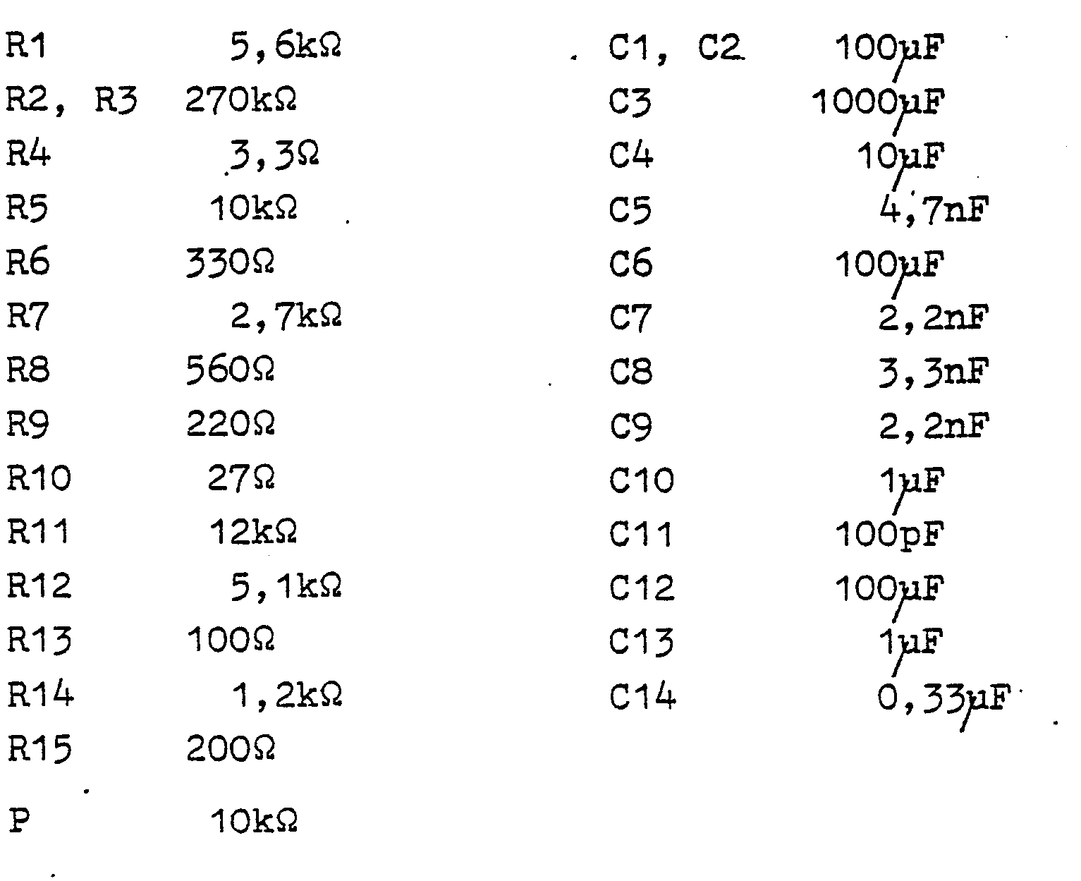
- Im folgenden ist eine bevorzugte Dimensionierung der Bauelemente des in der Figur dargestellten Ausführungsbeispiels angeführt:

- Die in der Figur dargestellte Schaltungsanordnung ist für maximale Ausgangsleistungen bis zu 30W ausgelegt. Sie läßt sich vorzugsweise in einem Miniatur-Schaltnetzteil einsetzen. Für die erfindungsgemäße Schaltungsanordnung bieten sich eine Reihe von Einsatzmöglichkeiten an, beispeilsweise als Stromversorgung für Videorecorder, Videokameras, Kamerarecorder, große Radio-Recorder, Hifi-Komponenten, Schreibmaschinen, Kopierer, Personal- und Home-Computer, Floppi-Disc-Laufwerke, Printer und Plotter . sowie Meß- und Prüfgeräte. Eine weitere Anwendungsmöglichkeit besteht bei Ladegeräten mit stabilisierter Ausgangsspannung für Blei- und NC-Akkumulatoren, insbesondere zur Schnelladung von NC-Sinterzellen, wobei Geräte mit entladenen Akkumulatoren mit eingestecktem Ladegerät sofort weiterbenutzt werden können. Diese Ladegeräte sind beispielsweise für Video-Portables, Videokameras, Kamerarecorder, Photoblitzgeräte, Elektrowerkzeuge (Schrauber, Bohrer, Rasenscheren) Modellsportfahrzeuge (Elektroflug, Elektroautos, Sender- und Empfänger-Akkumulatoren), Krankenfahrstühle, PKW-Batterien sowie Aktentaschen-Computer, geeignet.
- 1 Figur
Claims (4)
dadurch gekennzeichnet, daß
Priority Applications (1)
| Application Number | Priority Date | Filing Date | Title |
|---|---|---|---|
| AT85101577T ATE38596T1 (de) | 1984-02-17 | 1985-02-13 | Schaltungsanordnung fuer ein sperrwandlerschaltnetzteil. |
Applications Claiming Priority (2)
| Application Number | Priority Date | Filing Date | Title |
|---|---|---|---|
| DE19843405833 DE3405833A1 (de) | 1984-02-17 | 1984-02-17 | Schaltungsanordnung fuer ein sperrwandler-schaltnetzteil |
| DE3405833 | 1984-02-17 |
Publications (3)
| Publication Number | Publication Date |
|---|---|
| EP0152913A2 true EP0152913A2 (de) | 1985-08-28 |
| EP0152913A3 EP0152913A3 (en) | 1985-09-25 |
| EP0152913B1 EP0152913B1 (de) | 1988-11-09 |
Family
ID=6228088
Family Applications (1)
| Application Number | Title | Priority Date | Filing Date |
|---|---|---|---|
| EP85101577A Expired EP0152913B1 (de) | 1984-02-17 | 1985-02-13 | Schaltungsanordnung für ein Sperrwandler-Schaltnetzteil |
Country Status (5)
| Country | Link |
|---|---|
| US (1) | US4617533A (de) |
| EP (1) | EP0152913B1 (de) |
| JP (1) | JP2631362B2 (de) |
| AT (1) | ATE38596T1 (de) |
| DE (1) | DE3405833A1 (de) |
Families Citing this family (6)
| Publication number | Priority date | Publication date | Assignee | Title |
|---|---|---|---|---|
| DE3502324A1 (de) * | 1985-01-24 | 1986-07-24 | Siemens AG, 1000 Berlin und 8000 München | Sperrwandler-schaltnetzteil mit einem vor ueberspannungen geschuetzten schalttransistor |
| DE4238808C2 (de) * | 1992-11-17 | 1996-12-19 | Siemens Ag | Sperrwandler-Schaltnetzteil mit sinusförmiger Stromaufnahme |
| US5627738A (en) * | 1995-05-19 | 1997-05-06 | Eni, A Division Of Astec America, Inc. | Low cost, high reliability soft start arrangement |
| JP2006262610A (ja) * | 2005-03-16 | 2006-09-28 | Mitsumi Electric Co Ltd | 電源回路 |
| DE102005040543A1 (de) * | 2005-08-26 | 2007-03-01 | Siemens Ag | Stromrichterschaltung mit verteilten Energiespeichern |
| TR201909186T4 (tr) * | 2012-01-19 | 2019-07-22 | Koninklijke Philips Nv | Güç kaynağı cihazı. |
Family Cites Families (3)
| Publication number | Priority date | Publication date | Assignee | Title |
|---|---|---|---|---|
| US4045711A (en) * | 1976-03-19 | 1977-08-30 | Gte Sylvania Incorporated | Tuned oscillator ballast circuit |
| DE3032034A1 (de) * | 1980-08-25 | 1982-03-25 | Siemens Ag | Sperrschwinger-schaltnetzteil |
| DE3341785A1 (de) * | 1983-11-18 | 1985-06-13 | Siemens Ag | Miniatur-schaltnetzteil |
-
1984
- 1984-02-17 DE DE19843405833 patent/DE3405833A1/de active Granted
-
1985
- 1985-02-13 EP EP85101577A patent/EP0152913B1/de not_active Expired
- 1985-02-13 AT AT85101577T patent/ATE38596T1/de not_active IP Right Cessation
- 1985-02-14 US US06/701,391 patent/US4617533A/en not_active Expired - Fee Related
- 1985-02-15 JP JP60028159A patent/JP2631362B2/ja not_active Expired - Lifetime
Also Published As
| Publication number | Publication date |
|---|---|
| US4617533A (en) | 1986-10-14 |
| JP2631362B2 (ja) | 1997-07-16 |
| DE3405833C2 (de) | 1991-11-28 |
| ATE38596T1 (de) | 1988-11-15 |
| DE3405833A1 (de) | 1985-08-22 |
| JPS60194759A (ja) | 1985-10-03 |
| EP0152913B1 (de) | 1988-11-09 |
| EP0152913A3 (en) | 1985-09-25 |
Similar Documents
| Publication | Publication Date | Title |
|---|---|---|
| DE2756799C2 (de) | Fremdgetakteter, tastverhältnisgeregelter Gleichspannungswandler | |
| EP0531780B1 (de) | Schaltungsanordnung für ein freischwingendes Sperrwandler-Schaltnetzteil | |
| DE2728608A1 (de) | Gleichspannungswandler | |
| EP0095072A1 (de) | Elektronisches Schaltnetzteil | |
| EP0124734B1 (de) | Sperrwandler-Schaltnetzteil | |
| DE3335153C2 (de) | ||
| EP0734613B1 (de) | Schaltnetzteil | |
| EP0226128B2 (de) | Elektronisches Schaltnetzteil | |
| EP0380033A2 (de) | Schaltungsanordnung für ein freischwingendes Sperrwandler-Schaltnetzteil | |
| DE3123804C2 (de) | ||
| EP0135119B1 (de) | Sperrwandler-Schaltnetzteil | |
| DE3101375C2 (de) | Schaltungsanordnung zur geregelten Speisung eines Verbrauchers | |
| DE4023612A1 (de) | Spannungsversorgungsschaltung | |
| EP0167194A1 (de) | Schaltungsanordnung zur Versorgung der Regel- und Steuereinrichtung eines geregelten Gleichspannungswandlers | |
| EP0057910B2 (de) | Schaltung zur geregelten Speisung eines Verbrauchers | |
| EP0152913B1 (de) | Schaltungsanordnung für ein Sperrwandler-Schaltnetzteil | |
| EP0139226B1 (de) | Sperrwandler-Schaltnetzteil | |
| EP0219735B1 (de) | Schaltungsanordnung zur Spitzenstromreduzierung in einem Sperrwandler-Schaltnetzteil | |
| EP1206830A1 (de) | Schaltnetzteil mit einrichtung zur begrenzung der ausgangsspannung | |
| DE3720197C2 (de) | ||
| DE2804694A1 (de) | Getaktetes netzgeraet | |
| DE3347930A1 (de) | Schaltungsanordnung fuer ein sperrwandler-schaltnetzteil | |
| DE3311737C2 (de) | Elektronisches Schaltnetzteil | |
| EP0382307A2 (de) | Getaktete Stromversorgungseinrichtung | |
| EP0232915B1 (de) | Schaltungsanordnung einer auf Resonanz basierenden Gleichspannungsquelle |
Legal Events
| Date | Code | Title | Description |
|---|---|---|---|
| PUAI | Public reference made under article 153(3) epc to a published international application that has entered the european phase |
Free format text: ORIGINAL CODE: 0009012 |
|
| PUAL | Search report despatched |
Free format text: ORIGINAL CODE: 0009013 |
|
| AK | Designated contracting states |
Designated state(s): AT FR GB IT NL |
|
| AK | Designated contracting states |
Designated state(s): AT FR GB IT NL |
|
| 17P | Request for examination filed |
Effective date: 19860314 |
|
| 17Q | First examination report despatched |
Effective date: 19870401 |
|
| GRAA | (expected) grant |
Free format text: ORIGINAL CODE: 0009210 |
|
| AK | Designated contracting states |
Kind code of ref document: B1 Designated state(s): AT FR GB IT NL |
|
| REF | Corresponds to: |
Ref document number: 38596 Country of ref document: AT Date of ref document: 19881115 Kind code of ref document: T |
|
| GBT | Gb: translation of ep patent filed (gb section 77(6)(a)/1977) | ||
| ET | Fr: translation filed | ||
| ITF | It: translation for a ep patent filed | ||
| PLBE | No opposition filed within time limit |
Free format text: ORIGINAL CODE: 0009261 |
|
| STAA | Information on the status of an ep patent application or granted ep patent |
Free format text: STATUS: NO OPPOSITION FILED WITHIN TIME LIMIT |
|
| 26N | No opposition filed | ||
| ITTA | It: last paid annual fee | ||
| PGFP | Annual fee paid to national office [announced via postgrant information from national office to epo] |
Ref country code: GB Payment date: 19970123 Year of fee payment: 13 |
|
| PGFP | Annual fee paid to national office [announced via postgrant information from national office to epo] |
Ref country code: AT Payment date: 19970129 Year of fee payment: 13 |
|
| PGFP | Annual fee paid to national office [announced via postgrant information from national office to epo] |
Ref country code: NL Payment date: 19970225 Year of fee payment: 13 Ref country code: FR Payment date: 19970225 Year of fee payment: 13 |
|
| PG25 | Lapsed in a contracting state [announced via postgrant information from national office to epo] |
Ref country code: GB Free format text: LAPSE BECAUSE OF NON-PAYMENT OF DUE FEES Effective date: 19980213 Ref country code: AT Free format text: LAPSE BECAUSE OF NON-PAYMENT OF DUE FEES Effective date: 19980213 |
|
| PG25 | Lapsed in a contracting state [announced via postgrant information from national office to epo] |
Ref country code: FR Free format text: THE PATENT HAS BEEN ANNULLED BY A DECISION OF A NATIONAL AUTHORITY Effective date: 19980228 |
|
| PG25 | Lapsed in a contracting state [announced via postgrant information from national office to epo] |
Ref country code: NL Free format text: LAPSE BECAUSE OF NON-PAYMENT OF DUE FEES Effective date: 19980901 |
|
| GBPC | Gb: european patent ceased through non-payment of renewal fee |
Effective date: 19980213 |
|
| NLV4 | Nl: lapsed or anulled due to non-payment of the annual fee |
Effective date: 19980901 |
|
| REG | Reference to a national code |
Ref country code: FR Ref legal event code: ST |