EP0147656B1 - Multimicroprocesseur pour la commande d'une mémoire commune - Google Patents
Multimicroprocesseur pour la commande d'une mémoire commune Download PDFInfo
- Publication number
- EP0147656B1 EP0147656B1 EP19840114426 EP84114426A EP0147656B1 EP 0147656 B1 EP0147656 B1 EP 0147656B1 EP 19840114426 EP19840114426 EP 19840114426 EP 84114426 A EP84114426 A EP 84114426A EP 0147656 B1 EP0147656 B1 EP 0147656B1
- Authority
- EP
- European Patent Office
- Prior art keywords
- memory
- microprocessor
- data
- microprocessors
- control processor
- Prior art date
- Legal status (The legal status is an assumption and is not a legal conclusion. Google has not performed a legal analysis and makes no representation as to the accuracy of the status listed.)
- Expired
Links
Images


Classifications
-
- G—PHYSICS
- G06—COMPUTING OR CALCULATING; COUNTING
- G06F—ELECTRIC DIGITAL DATA PROCESSING
- G06F15/00—Digital computers in general; Data processing equipment in general
- G06F15/76—Architectures of general purpose stored program computers
- G06F15/80—Architectures of general purpose stored program computers comprising an array of processing units with common control, e.g. single instruction multiple data processors
- G06F15/8007—Architectures of general purpose stored program computers comprising an array of processing units with common control, e.g. single instruction multiple data processors single instruction multiple data [SIMD] multiprocessors
-
- G—PHYSICS
- G06—COMPUTING OR CALCULATING; COUNTING
- G06F—ELECTRIC DIGITAL DATA PROCESSING
- G06F12/00—Accessing, addressing or allocating within memory systems or architectures
- G06F12/02—Addressing or allocation; Relocation
- G06F12/0223—User address space allocation, e.g. contiguous or non contiguous base addressing
-
- G—PHYSICS
- G06—COMPUTING OR CALCULATING; COUNTING
- G06F—ELECTRIC DIGITAL DATA PROCESSING
- G06F13/00—Interconnection of, or transfer of information or other signals between, memories, input/output devices or central processing units
- G06F13/14—Handling requests for interconnection or transfer
- G06F13/16—Handling requests for interconnection or transfer for access to memory bus
- G06F13/1605—Handling requests for interconnection or transfer for access to memory bus based on arbitration
- G06F13/1652—Handling requests for interconnection or transfer for access to memory bus based on arbitration in a multiprocessor architecture
- G06F13/1663—Access to shared memory
Definitions
- the present invention is directed to multistation data processing systems, and more particularly to systems wherein multiple intelligent terminals share a large common memory.
- a single sequential-type controller is typically used, such as a high speed 370 (e.g., a 3081) processor.
- the processor When a request for data is received, the processor must search the memory contents to determine if the requested record has been stored and, if not, request a data transfer from a backing store, e.g., a disc, to the primary memory.
- a backing store e.g., a disc
- the sequential controller must process each request in sequence, and the system must therefore either use a very high speed processor, resulting in substantial cost increase, or use a less expensive and lower speed processor, resulting in unsatisfactory delays in memory access. Examples of such prior known systems are given below.
- US-A-4 253 144 describes such a multiprocessor system employing a large common memory.
- the processors are connected in a network for communication between the processors and to one or more global memory modules whereby memory resources may be shared by multi processor systems and where control and communications are provided between the processors through said global memory modules.
- EP-A-61 585 describes a data processing system having multiple data storage devices and a storage device management facility.
- the management facility maintains a single table recording for each logically active storage device. Allocation of space of storage devices to host processes is based on free or unallocated space in each such device.
- a high speed sequential memory controller is not required in order to obtain satisfactory access times even during a high volume of operations.
- the shared memory may comprise a large, page-formatted memory divided into a plurality of areas.
- the memory control function is distributed across an array of dedicated microprocessors, each of which is assigned to a specific area of the shared memory.
- Each microprocessor maintains the status of its assigned area in its own local storage, and can thus respond faster and with less variation in response time than a more powerful and more expensive serial controller which would have to manage the entire shared storage.
- the storage control function is achieved by a microprocessor array and a control processor.
- the control processor Upon receiving a request for data from one of the terminals in the system, the control processor will hash the requested virtual address to determine which of the microprocessors, if any, in the array, would be storing the requested data. The control processor then forwards the data request to that microprocessor which examines a directory table maintained in its own internal memory to determine if the requested data is currently stored in the portion of the shared memory which has been assigned to that microprocessor. If so, the address of the requested data in the primary memory is sent back to the requesting terminal, and the requesting terminal can then access the shared memory directly to obtain the desired data.
- a command is sent to a memory controller to transfer the requested record from a backing store, e.g., a disc memory, to the primary memory and, upon completion of the transfer, the microprocessor then sends the new address of the requested data to the requesting terminal.
- a backing store e.g., a disc memory
- the microprocessor responsible for the requested data finds that the requested data is not presently stored in its assigned shared memory area but that there is insufficient free space in its assigned memory area to accommodate a transfer of the requested data from the disc, the microprocessor can either discard some of its current data, e.g., in accordance with a Least Recently Used (LRU) algorithm, or it can negotiate with neighboring microprocessors to "borrow" some of the shared memory space assigned to its neighbors.
- LRU Least Recently Used
- control processor which is part of the storage control function need not maintain a hashing table for determining which of the microprocessors in the array is responsible for a requested data, but instead the control processor can merely broadcast the data request to all microprocessors in the array. All microprocessors can then examine their directory tables to determine if they currently control the requested data, and an appropriate one of the microprocessors will send an acknowledgement back to the control processor to indicate that it does control the requested data and will subsequently send the primary memory address of the requested data back to the requesting terminal. If no microprocessor responds affirmatively to the data request broadcast, the control processor can then broadcast to all microprocessors a request for free space. Any microprocessor having available memory in the shared storage will inform the control processor, at which time the control processor will then select one of the microprocessors according to a suitable algorithm and assign control of the requested data to that microprocessor for storage in its assigned memory.
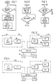
- Figure 1 is a general diagram of a data processing system in which use of the memory control system according to the present invention is contemplated.
- a plurality of intelligent terminals 10 are connected to respective ports of a switch 12.
- Each of the terminals 10 may be, e.g., a personal computer such as an IBM PC.
- the terminals 10 are each coupled to the switch 12 through a respective mapping box 14 which is provided solely for purposes of address translation.
- a variety of devices and circuits may be connected to respective ports of the switch 12, e.g., a print server 16, file server 18, memory 20, shared mainframe 22, etc.
- One of the ports of the switch 12 may also be coupled to a network gateway generally illustrated by block 24.
- the switch 12 is preferably a non-blocking type switch which can operate to selectively connect any of its ports to one another.
- any one of the cluster of intelligent terminals 10 illustrated in Figure 1 may have access to the print server 16, the file server 18 or some other type of shared intelligence 22, e.g., an IBM 370 mainframe computer. Any of the terminals may also communicate with one another through the switch. Terminals which require frequent communications with one another or with a peripheral unit connected to the switch 12 will be connected to the switch as shown in Figure 1. If less frequent communications are desired with other terminals, such communications may be established through the network gateway 24 which may, e.g., be a connection to a local area network or may even be a connection to a second switch to which a further cluster of terminals are connected as shown in Figure 1.
- the network gateway 24 may, e.g., be a connection to a local area network or may even be a connection to a second switch to which a further cluster of terminals are connected as shown in Figure 1.
- the present invention concerns the design and operation of the memory, generally designated by reference numeral 20, which may include a primary memory, e.g., a random access memory (RAM) 26, a backing store 28, e.g., a disc storage device, and a controller 30.
- the primary memory 26 may be a large, page-formatted or segmented memory.
- a conventional system would use a fast serial machine to implement the needed control functions, using memory maps and/or hashing tables. In fact, this function is often performed by one or all of the intelligent terminals 10 using local tables that describe the status of the various pages in the shared memory.
- the present invention rather than using a single fast serial machine, uses a plurality of microprocessors to implement the required memory control, as will now be described in more detail with reference to Figures 2-7.
- FIG. 2 generally illustrates one arrangement of the multi-microprocessor system for controlling shared memory.
- the application processors (CPUs) 110 in Figure 2 correspond to the intelligent terminals 10 in Figure 1
- the switch 112 in Figure 2 generally corresponds to the non-blocking switch 12 in Figure 1
- the Shared Common Store (SCS) 120 corresponds to the primary memory 26 and secondary memory 28 in Figure 1
- the storage Control Function (SCF) 130 generally corresponds to the memory controller 30 illustrated in Figure 1.
- the SCF 130 would perform various memory control functions, e.g., maintaining a directory table of the contents of the shared memory, issuing commands for memory transfers, etc.
- the Shared Common Store 120 can include both a primary memory MP 126 and a secondary memory MS 128.
- a conventional smart memory controller MC 132 can control data transfers between the primary and secondary memories while maintaining communication with the SCF 130.
- the SCF 130 can include a microprocessor array 134 and a control processor 136.
- the microprocessor array may be, e.g., an array of Z80 microprocessors available from Zilog or a plurality of 8086 microprocessors available from Intel.
- the control processor 136 could be an 8086 microprocessor. It should be appreciated that other microprocessors could be used as well.
- the primary memory 126 will be a large, page-formatted memory divided into a plurality of portions, and each of the microprocessors in the array 134 will be assigned to a respective portion, or area, in the primary memory 126.
- the plurality of microprocessors in the array 134 may be connected substantially as disclosed in copending Patent Application Serial No. 272,880, filed June 12, 1981.
- the microprocessors may be arranged as shown in Figures 4A and 4B.
- Each of the processors is connected via communications ports or channels 133 to each of its four immediate neighbors, and all microprocessors will also be connected to a common bus 135 for communicating with the control processor 136.
- Each microprocessor will include dual-ported local memory, e.g., with one R/W port and one RO port, or two R/W ports with a bus arbitrator. This will be described in more detail below.
- each microprocessor in the array 134 maintains in its own local storage the status, or a directory table, of its assigned area and can respond faster and more consistently than a more powerful serial controller which would have to manage the entire shared storage. Any request by a particular terminal 110 for a data record would be forwarded to the microprocessor array 134 which would then send back to the requesting terminal the address in the primary memory 126 at which the requested record could be found. The terminal 110 could then access the primary memory 126 directly through the switch 112. If the requested data record was not presently in the memory 126, a command would be sent from the microprocessor array 134 to the memory controller 132 to cause the memory controller 132 to transfer the requested record from the backing store 128 to the main memory 126. A signal indicating that the transfer had been completed would then be sent back to the microprocessor array, and the address of the requested record in the memory 126 would then be sent to the terminal 110.
- control processor 136 in the preferred embodiment of this invention acts essentially as an interface forwarding messages between the switch 112, microprocessor array 134 and memory controller 32. Messages from the memory controller 132 or switch 112 are forwarded to the microprocessor array 134, and messages from the microprocessor array 134 are forwarded to the switch 112 or memory controller 132 as appropriate.
- the operation of the microprocessor array 134 will now be described in more detail.
- the data request is connected through the switch 112 to the control processor 136 which then forwards the request to a specific microprocessor in the array 134 by hashing the requested address.
- the particular microprocessor to which the request is forwarded will determine at step 200 in Figure 6A that the received message is a request for data by a terminal, and the microprocessor will check its page table to find out if the requested record is stored in the area of memory which has been assigned to that microprocessor.
- the microprocessor at step 202 sends back to the requesting terminal, via the control processor 136 and switch 112, the address in the memory 126 at which the requested data can be found.
- the terminal 110 can then access the memory 126 directly through the switch 112.
- the microprocessor will determine if there is sufficient free space in its partition, i.e., in the area of the memory 126 assigned to that microprocessor, to store the requested record. If so, the microprocessor sends a command to the memory controller 132 to transfer the data from the backing store 128 to a particular address in the primary memory 126. The microprocessor then returns to the beginning of the program in Figure 6A. As soon as the data transfer has been completed by the memory controller 132, a signal to that effect is sent via the control processor 136 to the appropriate microprocessor which then determines at step 204 that the data transfer has been completed. The address of the requested data in the memory 126 is then sent to the requesting terminal.
- the microprocessor determines at step 206 that there is insufficient free space in its assigned memory partition to store the requested record, it must either transfer some of its current memory content to the backing store in order to make room for the newly requested record, or it must obtain the use of some additional memory space. In most cases the latter option is preferred, and the microprocessor at step 208 sends a request over the common communication channels 133 to its immediate neighbors requesting negotiation. When a response is received from a neighbor, the microprocessor then negotiates with that neighbor to determine if the neighboring microprocessor has any space in its own assigned memory partition that it would be willing to relinquish.
- the space negotiation is considered successful and the microprocessor sends to the memory controller 132 a request to transfer the requested data from the backing store to the memory 126.
- the microprocessor then returns to the beginning of the program in Figure 6A and again awaits a signal from the memory controller indicating that the data transfer has been completed.
- the microprocessor determines which page should be discarded, and this can be done according to any one of a number of known criteria, e.g., according to a Least Recently Used (LRU) algorithm.
- LRU Least Recently Used
- the microprocessor cannot merely dump a page from its memory partition, since the terminal which last requested that page may currently be accessing the page directly through the switch 112. Accordingly, when the microprocessor determines that a page should be discarded, it sends a signal to the terminal last requesting that page to indicate that the page is no longer in memory.
- the microprocessor then returns to the beginning of the program in Figure 6A and awaits acknowledgement from the terminal. As soon as an acknowlegement is received, the microprocessor program advances to step 210 in Figure 6A and sends a data transfer command to the memory controller to cause the discarded data to be written out to the backing store 128 and the newly requested data to be written from the backing store 128 to the appropriate address locations in the memory 126. The microprocessor then returns to the beginning of the program to await a signal from the memory controller that the data transfer has been completed, at which time the new address location of the requested data is forwarded via the control processor 136 and switch 112 to the requesting terminal 110.
- the function of the controller 132 is merely to process data transfer requests and to send completion signals back to the control processor 136. This is generally illustrated in the flow chart of Figure 7.
- the memory controller may be a conventional smart disc controller, and its detailed operation will be well understood to those of skill in the art.
- control processor 136 hash the data address in order to determine particular microprocessor in the array 134 which should control that record. However, if hashing is not practical, then a broadcast algorithm can be used.
- each microprocessor at step 200 will also be capable of detecting when a message is a broadcast page number requiring a response.
- the microprocessor will test to see if it does control that page and, if so, will send back a response to the control processor indicating that it does control that page.
- the control processor receiving a response indicating that a particular microprocessor controls the requested page, will then forward the message to that microprocessor at step 214 in Figure 5.
- the additional steps in the control processor flow chart for broadcast operation are shown in Figure 8, and the additional steps to be added to the microprocessor flow chart of Figure 6A for broadcast operation are illustrated in Figure 9.
- an alternative technique for broadcast operation would be for the control processor, after broadcasting the page number to all microprocessors as shown in the flow chart portion of Figure 8, to return to the beginning of the control processor program in Figure 5 and await an acknowledgement message from the responsible microprocessor.
- a third destination choice branching from step 213 in Figure 5 would be that the message is from a microprocessor and is directed to the control processor as an acknowledgement of page responsibility.
- the control processor could then forward the data request message to the acknowledging microprocessor.
- the control processor when no response is received from any microprocessor indicating that it controls the requested page, the control processor knows that a new page is needed. In such a case, the controller will broadcast a request for a new page to all of the elements in the microprocessor array. All elements that have free pages available will respond with their identification numbers on a common bus. In a case of multiple free pages, the controller would use a suitable minimum finding algorithm for selecting one of the free pages. If only one copy of a page exists in memory at a time, the controller can broadcast the request for access to that page knowing that only the proper array element will respond. Duplicate copies of a page and/or data and code sharing (synonym problem) can also be handled using this technique.
- the same microprocessor will acknowledge responsibility for the page and will then request the memory controller 132 to transfer the page from the backing store 128 to the primary memory 126, again in a manner substantially the same as described above with reference to the hashing embodiment.
- the microprocessor may receive a subsequent request for that data at a time when it does not have sufficient space in its assigned area of the primary memory 126. In such a case, the microprocessor will either borrow some memory space assigned to one of its neighbors or will discard some of the data currently stored in its assigned primary memory area in order to make room for the newly requested data. Both of these procedures will be performed in substantially the same manner as described above with reference to the hashing embodiment of the invention.
- the hashing mode of operation i.e. the embodiment of the present invention wherein the control processor 136 would hash the requested data address in order to determine the responsible microprocessor in the array 134, would normally be more efficient than the broadcast mode, but the broadcast mode of operation would be advantageous in that it would permit more efficient balancing of the loading of individual microprocessors in the array 134. This can be understood by examining the two techniques more closely. With reference first to the hashing technique, each microprocessor in the array 134 would be assigned responsibility not only for a respective area of the primary memory 126 but also for a respective area of the virtual address space.
- the virtual address would be hashed to determine the responsible microprocessor, and each time a particular record of data is requested it would always be considered the responsibility of the same microprocessor.
- the responsible microprocessor would therefore always be determined quickly, and the hashing mode of operation would be more efficient in this regard.
- a data request would be broadcast to all microprocessors in the array 134, and the responsible microprocessor would acknowledge. If no microprocessor acknowledged responsibility, the control processor would then have to ask for free page availability and would then have to assign responsibility to an appropriate one of the responding microprocessors. This would be a somewhat slower technique for determining the responsibility for a requested page, but the load balancing advantages should be easily appreciated. More particularly, rather than requiring that the same microprocessor always have responsibility for a particular page as in the hashing technique, the broadcast technique would permit assignment of responsibility to any microprocessor in the array in accordance with the loading of the microprocessors at the time of the original request.
- the loading balancing feature of the broadcast mode of operation would be useful not only in assigning responsibility for new pages, but could be utilized on a continuing basis as follows. If a first microprocessor finds that its directory table, or list, is becoming undesirably long, the first microprocessor may communicate with one of its neighbors to see if a neighbor will accept responsibility for one of the pages for which the first microprocessor is currently responsible. If a neighboring microprocessor does not have an excessively long list, it may accept responsibility for one or more data pages, and the neighboring microprocessor will then acknowledge responsibility for that page upon all feature requests.
- control processor could send out a request asking that all microprocessors examine the page tables in their neighbor microprocessors to insure that a microprocessor had not failed and was merely failing to respond.
- the intelligent disc controller MC will be physically located within the Shared Common Store, since there are several configurations in which the application CPU's must communicate with the main memory 126 through the controller 132.
- the primary memory MP is dual-ported to provide direct access by the application CPUs 110 to the memory 126 through the switch 112. Alternative arrangements may be used, however, several examples of which are illustrated in Figures 10-13.
- the management of the memory 126 is shared by a plurality of microprocessors.
- the memory 126 can therefore be made quite large without encountering excessive memory access delays which would result if a single memory controller were used which would have to process all data requests in a serial manner and which would be required to manage the entire shared storage by itself.
- a controller with 64 independent element microprocessors The memory system would be presented with a virtual address and would have to determine whether any page currently in the shared storage has been mapped onto this virtual address, even though it may have been brought in under some other identifier.
- the system according to the present invention divides the total number of pages in the shared memory into 64 roughly equal sets, and each set would be examined independently and concurrently by its own dedicated microprocessor.
- a sequential processor based controller would have to be 64 times as fast as one microprocessor element of the present invention in order to achieve equivalent performance.
- the present invention results in a large economic advantage with respect to conventional sequential processors, since the control is achieved by a combination of identical inexpensive microprocessors, each of which can be implemented as a high-volume production item. This is made possible by VLSI technology. Since there can be 64 or more microprocessors in such a structure, each can be reasonably slow. This makes a sophisticated cooling and power distributed network unnecessary, substantially reducing the control function costs. In the near future, VLSI technology can be expected to provide 1 MIP (1 million instructions per second) microprocessors costing between $10.00 and $20.00 each, at high volume.
- interconnection between microprocessors and the array is the ability to consult a neighboring microprocessor to negotiate for space in case of overflows
- this interconnection also permits individual element microprocessors to perform extensive local computations to guarantee correctness or to enhance performance without significantly degrading the response of the overall shared-memory unit.
- a main advantage of this approach is that the availability of the shared storage unit is largely unaffected by ancillary processing required for recovery, journalling, look-head cast- outs, or prefetching, etc.
- the central processor is free to process additional requests from other application processors 110 immediately after forwarding, unless serialization is required (e.g., journalling of non-volatile permanent data).
- the local element microprocessor updates any status change to its assigned pages/ segments, and performs any required data transfers using the common bus. This processing and transfer activity is asynchronous with respect to the central control processor, all application processors, and other element microprocessors.
Landscapes
- Engineering & Computer Science (AREA)
- Theoretical Computer Science (AREA)
- Physics & Mathematics (AREA)
- General Engineering & Computer Science (AREA)
- General Physics & Mathematics (AREA)
- Computer Hardware Design (AREA)
- Computing Systems (AREA)
- Multi Processors (AREA)
- Memory System Of A Hierarchy Structure (AREA)
- Memory System (AREA)
Claims (9)
Applications Claiming Priority (2)
| Application Number | Priority Date | Filing Date | Title |
|---|---|---|---|
| US56730483A | 1983-12-30 | 1983-12-30 | |
| US567304 | 1995-12-05 |
Publications (3)
| Publication Number | Publication Date |
|---|---|
| EP0147656A2 EP0147656A2 (fr) | 1985-07-10 |
| EP0147656A3 EP0147656A3 (en) | 1987-12-02 |
| EP0147656B1 true EP0147656B1 (fr) | 1990-01-17 |
Family
ID=24266622
Family Applications (1)
| Application Number | Title | Priority Date | Filing Date |
|---|---|---|---|
| EP19840114426 Expired EP0147656B1 (fr) | 1983-12-30 | 1984-11-30 | Multimicroprocesseur pour la commande d'une mémoire commune |
Country Status (3)
| Country | Link |
|---|---|
| EP (1) | EP0147656B1 (fr) |
| JP (1) | JPH0642238B2 (fr) |
| DE (1) | DE3481092D1 (fr) |
Families Citing this family (3)
| Publication number | Priority date | Publication date | Assignee | Title |
|---|---|---|---|---|
| JPS63225848A (ja) * | 1987-03-16 | 1988-09-20 | Agency Of Ind Science & Technol | 計算機システム |
| AT395202B (de) * | 1989-12-13 | 1992-10-27 | Haider Gottfried Dipl Ing | Drehkolbenverdichter |
| JP3057934B2 (ja) * | 1992-10-30 | 2000-07-04 | 日本電気株式会社 | 共有バス調停機構 |
Family Cites Families (4)
| Publication number | Priority date | Publication date | Assignee | Title |
|---|---|---|---|---|
| US4253144A (en) * | 1978-12-21 | 1981-02-24 | Burroughs Corporation | Multi-processor communication network |
| US4365292A (en) * | 1979-11-26 | 1982-12-21 | Burroughs Corporation | Array processor architecture connection network |
| JPS57105055A (en) * | 1980-12-23 | 1982-06-30 | Fujitsu Ltd | Main storage access system |
| US4528624A (en) * | 1981-03-25 | 1985-07-09 | International Business Machines Corporation | Method and apparatus for allocating memory space based upon free space in diverse memory devices |
-
1984
- 1984-11-20 JP JP59243556A patent/JPH0642238B2/ja not_active Expired - Lifetime
- 1984-11-30 DE DE8484114426T patent/DE3481092D1/de not_active Expired - Lifetime
- 1984-11-30 EP EP19840114426 patent/EP0147656B1/fr not_active Expired
Also Published As
| Publication number | Publication date |
|---|---|
| JPS60147861A (ja) | 1985-08-03 |
| JPH0642238B2 (ja) | 1994-06-01 |
| EP0147656A3 (en) | 1987-12-02 |
| DE3481092D1 (de) | 1990-02-22 |
| EP0147656A2 (fr) | 1985-07-10 |
Similar Documents
| Publication | Publication Date | Title |
|---|---|---|
| US4881164A (en) | Multi-microprocessor for controlling shared memory | |
| EP0709779B1 (fr) | Disques virtuels partagés avec récupération transparente pour l'application | |
| EP0166268B1 (fr) | Accès à mémoire partagée pour système de traitement de données | |
| US5548724A (en) | File server system and file access control method of the same | |
| US5117350A (en) | Memory address mechanism in a distributed memory architecture | |
| US5991797A (en) | Method for directing I/O transactions between an I/O device and a memory | |
| US6108684A (en) | Methods and apparatus for balancing loads on a storage subsystem among a plurality of controllers | |
| US6751703B2 (en) | Data storage systems and methods which utilize an on-board cache | |
| EP0258736B1 (fr) | Calculateur parallèle à mémoires partagées distribuées et circuits partagés pour activer des tâches | |
| EP0106213B1 (fr) | Système décentralisé de traitement d'information et procédé d'introduction initiale du programme y relatif | |
| US6173374B1 (en) | System and method for peer-to-peer accelerated I/O shipping between host bus adapters in clustered computer network | |
| US5335327A (en) | External memory control techniques with multiprocessors improving the throughput of data between a hierarchically upper processing unit and an external memory with efficient use of a cache memory | |
| US20040230750A1 (en) | Memory management for a symmetric multiprocessor computer system | |
| WO2002008899A2 (fr) | Procede et appareil permettant la realisation de systemes de traitement et de memoire de donnees de haute performance et extensibles | |
| US6356978B1 (en) | File control device | |
| JP3776496B2 (ja) | データ記憶システム | |
| US5708784A (en) | Dual bus computer architecture utilizing distributed arbitrators and method of using same | |
| CN118862123A (zh) | 一种共享内存区域的访问方法及计算设备 | |
| US6339812B1 (en) | Method and apparatus for handling invalidation requests to processors not present in a computer system | |
| EP0147656B1 (fr) | Multimicroprocesseur pour la commande d'une mémoire commune | |
| US20030014599A1 (en) | Method for providing a configurable primary mirror | |
| JP3719976B2 (ja) | 二重化コントローラ構成ディスク記憶システム向けコントローラ、及び同コントローラが二重化されたディスク記憶システム | |
| KR100198808B1 (ko) | 저장용 미디어간의 직접 자료 복사 방법 | |
| US6877029B1 (en) | Method and apparatus for managing node controllers using partitions in a computer system | |
| JP2664827B2 (ja) | 実時間情報転送制御方法 |
Legal Events
| Date | Code | Title | Description |
|---|---|---|---|
| PUAI | Public reference made under article 153(3) epc to a published international application that has entered the european phase |
Free format text: ORIGINAL CODE: 0009012 |
|
| 17P | Request for examination filed |
Effective date: 19841214 |
|
| AK | Designated contracting states |
Designated state(s): DE FR GB |
|
| PUAL | Search report despatched |
Free format text: ORIGINAL CODE: 0009013 |
|
| AK | Designated contracting states |
Kind code of ref document: A3 Designated state(s): DE FR GB |
|
| 17Q | First examination report despatched |
Effective date: 19880620 |
|
| GRAA | (expected) grant |
Free format text: ORIGINAL CODE: 0009210 |
|
| AK | Designated contracting states |
Kind code of ref document: B1 Designated state(s): DE FR GB |
|
| REF | Corresponds to: |
Ref document number: 3481092 Country of ref document: DE Date of ref document: 19900222 |
|
| ET | Fr: translation filed | ||
| PLBE | No opposition filed within time limit |
Free format text: ORIGINAL CODE: 0009261 |
|
| STAA | Information on the status of an ep patent application or granted ep patent |
Free format text: STATUS: NO OPPOSITION FILED WITHIN TIME LIMIT |
|
| 26N | No opposition filed | ||
| PGFP | Annual fee paid to national office [announced via postgrant information from national office to epo] |
Ref country code: GB Payment date: 19951024 Year of fee payment: 12 |
|
| PGFP | Annual fee paid to national office [announced via postgrant information from national office to epo] |
Ref country code: FR Payment date: 19951107 Year of fee payment: 12 |
|
| PGFP | Annual fee paid to national office [announced via postgrant information from national office to epo] |
Ref country code: DE Payment date: 19951123 Year of fee payment: 12 |
|
| PG25 | Lapsed in a contracting state [announced via postgrant information from national office to epo] |
Ref country code: GB Effective date: 19961130 |
|
| GBPC | Gb: european patent ceased through non-payment of renewal fee |
Effective date: 19961130 |
|
| PG25 | Lapsed in a contracting state [announced via postgrant information from national office to epo] |
Ref country code: FR Effective date: 19970731 |
|
| PG25 | Lapsed in a contracting state [announced via postgrant information from national office to epo] |
Ref country code: DE Effective date: 19970801 |
|
| REG | Reference to a national code |
Ref country code: FR Ref legal event code: ST |