EP0147576B1 - Process for forming elongated solder connections between a semiconductor device and a supporting substrate - Google Patents
Process for forming elongated solder connections between a semiconductor device and a supporting substrate Download PDFInfo
- Publication number
- EP0147576B1 EP0147576B1 EP84113328A EP84113328A EP0147576B1 EP 0147576 B1 EP0147576 B1 EP 0147576B1 EP 84113328 A EP84113328 A EP 84113328A EP 84113328 A EP84113328 A EP 84113328A EP 0147576 B1 EP0147576 B1 EP 0147576B1
- Authority
- EP
- European Patent Office
- Prior art keywords
- solder
- semiconductor device
- pads
- supporting substrate
- substrate
- Prior art date
- Legal status (The legal status is an assumption and is not a legal conclusion. Google has not performed a legal analysis and makes no representation as to the accuracy of the status listed.)
- Expired
Links
- 229910000679 solder Inorganic materials 0.000 title claims description 84
- 239000000758 substrate Substances 0.000 title claims description 71
- 239000004065 semiconductor Substances 0.000 title claims description 29
- 238000000034 method Methods 0.000 title claims description 28
- 230000008569 process Effects 0.000 title claims description 18
- 239000004606 Fillers/Extenders Substances 0.000 claims description 26
- 229910052751 metal Inorganic materials 0.000 claims description 15
- 239000002184 metal Substances 0.000 claims description 15
- 238000002844 melting Methods 0.000 claims description 11
- 230000008018 melting Effects 0.000 claims description 11
- 238000010438 heat treatment Methods 0.000 claims description 5
- 238000001816 cooling Methods 0.000 claims description 4
- 238000000151 deposition Methods 0.000 claims description 4
- 239000011521 glass Substances 0.000 claims description 4
- 238000005245 sintering Methods 0.000 claims description 4
- 239000011248 coating agent Substances 0.000 claims description 3
- 238000000576 coating method Methods 0.000 claims description 3
- 229910020220 Pb—Sn Inorganic materials 0.000 claims 3
- 239000003870 refractory metal Substances 0.000 claims 1
- 238000007650 screen-printing Methods 0.000 claims 1
- XUIMIQQOPSSXEZ-UHFFFAOYSA-N Silicon Chemical compound [Si] XUIMIQQOPSSXEZ-UHFFFAOYSA-N 0.000 description 5
- 239000000463 material Substances 0.000 description 5
- 229910052710 silicon Inorganic materials 0.000 description 5
- 239000010703 silicon Substances 0.000 description 5
- 238000005272 metallurgy Methods 0.000 description 4
- 239000000919 ceramic Substances 0.000 description 3
- 238000004519 manufacturing process Methods 0.000 description 3
- 230000002093 peripheral effect Effects 0.000 description 3
- PXHVJJICTQNCMI-UHFFFAOYSA-N Nickel Chemical compound [Ni] PXHVJJICTQNCMI-UHFFFAOYSA-N 0.000 description 2
- 229910045601 alloy Inorganic materials 0.000 description 2
- 239000000956 alloy Substances 0.000 description 2
- 230000008901 benefit Effects 0.000 description 2
- 238000005304 joining Methods 0.000 description 2
- 238000012986 modification Methods 0.000 description 2
- 230000004048 modification Effects 0.000 description 2
- 238000007740 vapor deposition Methods 0.000 description 2
- RYGMFSIKBFXOCR-UHFFFAOYSA-N Copper Chemical compound [Cu] RYGMFSIKBFXOCR-UHFFFAOYSA-N 0.000 description 1
- ZOKXTWBITQBERF-UHFFFAOYSA-N Molybdenum Chemical compound [Mo] ZOKXTWBITQBERF-UHFFFAOYSA-N 0.000 description 1
- ATJFFYVFTNAWJD-UHFFFAOYSA-N Tin Chemical compound [Sn] ATJFFYVFTNAWJD-UHFFFAOYSA-N 0.000 description 1
- 230000004888 barrier function Effects 0.000 description 1
- 239000011230 binding agent Substances 0.000 description 1
- 230000015572 biosynthetic process Effects 0.000 description 1
- 229910010293 ceramic material Inorganic materials 0.000 description 1
- 239000004020 conductor Substances 0.000 description 1
- 238000010276 construction Methods 0.000 description 1
- 229910052802 copper Inorganic materials 0.000 description 1
- 239000010949 copper Substances 0.000 description 1
- 230000007423 decrease Effects 0.000 description 1
- 238000011161 development Methods 0.000 description 1
- 238000011982 device technology Methods 0.000 description 1
- 238000005516 engineering process Methods 0.000 description 1
- PCHJSUWPFVWCPO-UHFFFAOYSA-N gold Chemical compound [Au] PCHJSUWPFVWCPO-UHFFFAOYSA-N 0.000 description 1
- 229910052737 gold Inorganic materials 0.000 description 1
- 239000010931 gold Substances 0.000 description 1
- 230000006872 improvement Effects 0.000 description 1
- 239000000203 mixture Substances 0.000 description 1
- 229910052750 molybdenum Inorganic materials 0.000 description 1
- 239000011733 molybdenum Substances 0.000 description 1
- 230000007935 neutral effect Effects 0.000 description 1
- 229910052759 nickel Inorganic materials 0.000 description 1
- 239000004014 plasticizer Substances 0.000 description 1
- 239000011819 refractory material Substances 0.000 description 1
- 238000012827 research and development Methods 0.000 description 1
- 238000012216 screening Methods 0.000 description 1
- 229910052715 tantalum Inorganic materials 0.000 description 1
- GUVRBAGPIYLISA-UHFFFAOYSA-N tantalum atom Chemical compound [Ta] GUVRBAGPIYLISA-UHFFFAOYSA-N 0.000 description 1
- WFKWXMTUELFFGS-UHFFFAOYSA-N tungsten Chemical compound [W] WFKWXMTUELFFGS-UHFFFAOYSA-N 0.000 description 1
- 229910052721 tungsten Inorganic materials 0.000 description 1
- 239000010937 tungsten Substances 0.000 description 1
Images
Classifications
-
- H—ELECTRICITY
- H01—ELECTRIC ELEMENTS
- H01L—SEMICONDUCTOR DEVICES NOT COVERED BY CLASS H10
- H01L24/00—Arrangements for connecting or disconnecting semiconductor or solid-state bodies; Methods or apparatus related thereto
- H01L24/80—Methods for connecting semiconductor or other solid state bodies using means for bonding being attached to, or being formed on, the surface to be connected
- H01L24/81—Methods for connecting semiconductor or other solid state bodies using means for bonding being attached to, or being formed on, the surface to be connected using a bump connector
-
- H—ELECTRICITY
- H01—ELECTRIC ELEMENTS
- H01L—SEMICONDUCTOR DEVICES NOT COVERED BY CLASS H10
- H01L21/00—Processes or apparatus adapted for the manufacture or treatment of semiconductor or solid state devices or of parts thereof
- H01L21/02—Manufacture or treatment of semiconductor devices or of parts thereof
- H01L21/04—Manufacture or treatment of semiconductor devices or of parts thereof the devices having potential barriers, e.g. a PN junction, depletion layer or carrier concentration layer
- H01L21/48—Manufacture or treatment of parts, e.g. containers, prior to assembly of the devices, using processes not provided for in a single one of the subgroups H01L21/06 - H01L21/326
- H01L21/4814—Conductive parts
- H01L21/4846—Leads on or in insulating or insulated substrates, e.g. metallisation
- H01L21/4853—Connection or disconnection of other leads to or from a metallisation, e.g. pins, wires, bumps
-
- H—ELECTRICITY
- H01—ELECTRIC ELEMENTS
- H01L—SEMICONDUCTOR DEVICES NOT COVERED BY CLASS H10
- H01L23/00—Details of semiconductor or other solid state devices
- H01L23/48—Arrangements for conducting electric current to or from the solid state body in operation, e.g. leads, terminal arrangements ; Selection of materials therefor
- H01L23/488—Arrangements for conducting electric current to or from the solid state body in operation, e.g. leads, terminal arrangements ; Selection of materials therefor consisting of soldered or bonded constructions
- H01L23/498—Leads, i.e. metallisations or lead-frames on insulating substrates, e.g. chip carriers
- H01L23/49811—Additional leads joined to the metallisation on the insulating substrate, e.g. pins, bumps, wires, flat leads
-
- H—ELECTRICITY
- H01—ELECTRIC ELEMENTS
- H01L—SEMICONDUCTOR DEVICES NOT COVERED BY CLASS H10
- H01L24/00—Arrangements for connecting or disconnecting semiconductor or solid-state bodies; Methods or apparatus related thereto
- H01L24/01—Means for bonding being attached to, or being formed on, the surface to be connected, e.g. chip-to-package, die-attach, "first-level" interconnects; Manufacturing methods related thereto
- H01L24/10—Bump connectors ; Manufacturing methods related thereto
- H01L24/11—Manufacturing methods
-
- H—ELECTRICITY
- H01—ELECTRIC ELEMENTS
- H01L—SEMICONDUCTOR DEVICES NOT COVERED BY CLASS H10
- H01L24/00—Arrangements for connecting or disconnecting semiconductor or solid-state bodies; Methods or apparatus related thereto
- H01L24/01—Means for bonding being attached to, or being formed on, the surface to be connected, e.g. chip-to-package, die-attach, "first-level" interconnects; Manufacturing methods related thereto
- H01L24/10—Bump connectors ; Manufacturing methods related thereto
- H01L24/15—Structure, shape, material or disposition of the bump connectors after the connecting process
- H01L24/17—Structure, shape, material or disposition of the bump connectors after the connecting process of a plurality of bump connectors
-
- H—ELECTRICITY
- H05—ELECTRIC TECHNIQUES NOT OTHERWISE PROVIDED FOR
- H05K—PRINTED CIRCUITS; CASINGS OR CONSTRUCTIONAL DETAILS OF ELECTRIC APPARATUS; MANUFACTURE OF ASSEMBLAGES OF ELECTRICAL COMPONENTS
- H05K3/00—Apparatus or processes for manufacturing printed circuits
- H05K3/30—Assembling printed circuits with electric components, e.g. with resistor
- H05K3/32—Assembling printed circuits with electric components, e.g. with resistor electrically connecting electric components or wires to printed circuits
- H05K3/34—Assembling printed circuits with electric components, e.g. with resistor electrically connecting electric components or wires to printed circuits by soldering
- H05K3/341—Surface mounted components
- H05K3/3431—Leadless components
- H05K3/3436—Leadless components having an array of bottom contacts, e.g. pad grid array or ball grid array components
-
- H—ELECTRICITY
- H01—ELECTRIC ELEMENTS
- H01L—SEMICONDUCTOR DEVICES NOT COVERED BY CLASS H10
- H01L2224/00—Indexing scheme for arrangements for connecting or disconnecting semiconductor or solid-state bodies and methods related thereto as covered by H01L24/00
- H01L2224/01—Means for bonding being attached to, or being formed on, the surface to be connected, e.g. chip-to-package, die-attach, "first-level" interconnects; Manufacturing methods related thereto
- H01L2224/02—Bonding areas; Manufacturing methods related thereto
- H01L2224/04—Structure, shape, material or disposition of the bonding areas prior to the connecting process
- H01L2224/0401—Bonding areas specifically adapted for bump connectors, e.g. under bump metallisation [UBM]
-
- H—ELECTRICITY
- H01—ELECTRIC ELEMENTS
- H01L—SEMICONDUCTOR DEVICES NOT COVERED BY CLASS H10
- H01L2224/00—Indexing scheme for arrangements for connecting or disconnecting semiconductor or solid-state bodies and methods related thereto as covered by H01L24/00
- H01L2224/01—Means for bonding being attached to, or being formed on, the surface to be connected, e.g. chip-to-package, die-attach, "first-level" interconnects; Manufacturing methods related thereto
- H01L2224/02—Bonding areas; Manufacturing methods related thereto
- H01L2224/04—Structure, shape, material or disposition of the bonding areas prior to the connecting process
- H01L2224/06—Structure, shape, material or disposition of the bonding areas prior to the connecting process of a plurality of bonding areas
- H01L2224/0601—Structure
- H01L2224/0603—Bonding areas having different sizes, e.g. different heights or widths
-
- H—ELECTRICITY
- H01—ELECTRIC ELEMENTS
- H01L—SEMICONDUCTOR DEVICES NOT COVERED BY CLASS H10
- H01L2224/00—Indexing scheme for arrangements for connecting or disconnecting semiconductor or solid-state bodies and methods related thereto as covered by H01L24/00
- H01L2224/01—Means for bonding being attached to, or being formed on, the surface to be connected, e.g. chip-to-package, die-attach, "first-level" interconnects; Manufacturing methods related thereto
- H01L2224/10—Bump connectors; Manufacturing methods related thereto
- H01L2224/1012—Auxiliary members for bump connectors, e.g. spacers
- H01L2224/10122—Auxiliary members for bump connectors, e.g. spacers being formed on the semiconductor or solid-state body to be connected
- H01L2224/10135—Alignment aids
-
- H—ELECTRICITY
- H01—ELECTRIC ELEMENTS
- H01L—SEMICONDUCTOR DEVICES NOT COVERED BY CLASS H10
- H01L2224/00—Indexing scheme for arrangements for connecting or disconnecting semiconductor or solid-state bodies and methods related thereto as covered by H01L24/00
- H01L2224/01—Means for bonding being attached to, or being formed on, the surface to be connected, e.g. chip-to-package, die-attach, "first-level" interconnects; Manufacturing methods related thereto
- H01L2224/10—Bump connectors; Manufacturing methods related thereto
- H01L2224/1012—Auxiliary members for bump connectors, e.g. spacers
- H01L2224/10152—Auxiliary members for bump connectors, e.g. spacers being formed on an item to be connected not being a semiconductor or solid-state body
- H01L2224/10165—Alignment aids
-
- H—ELECTRICITY
- H01—ELECTRIC ELEMENTS
- H01L—SEMICONDUCTOR DEVICES NOT COVERED BY CLASS H10
- H01L2224/00—Indexing scheme for arrangements for connecting or disconnecting semiconductor or solid-state bodies and methods related thereto as covered by H01L24/00
- H01L2224/01—Means for bonding being attached to, or being formed on, the surface to be connected, e.g. chip-to-package, die-attach, "first-level" interconnects; Manufacturing methods related thereto
- H01L2224/10—Bump connectors; Manufacturing methods related thereto
- H01L2224/12—Structure, shape, material or disposition of the bump connectors prior to the connecting process
- H01L2224/13—Structure, shape, material or disposition of the bump connectors prior to the connecting process of an individual bump connector
- H01L2224/13001—Core members of the bump connector
- H01L2224/13099—Material
- H01L2224/131—Material with a principal constituent of the material being a metal or a metalloid, e.g. boron [B], silicon [Si], germanium [Ge], arsenic [As], antimony [Sb], tellurium [Te] and polonium [Po], and alloys thereof
-
- H—ELECTRICITY
- H01—ELECTRIC ELEMENTS
- H01L—SEMICONDUCTOR DEVICES NOT COVERED BY CLASS H10
- H01L2224/00—Indexing scheme for arrangements for connecting or disconnecting semiconductor or solid-state bodies and methods related thereto as covered by H01L24/00
- H01L2224/01—Means for bonding being attached to, or being formed on, the surface to be connected, e.g. chip-to-package, die-attach, "first-level" interconnects; Manufacturing methods related thereto
- H01L2224/10—Bump connectors; Manufacturing methods related thereto
- H01L2224/12—Structure, shape, material or disposition of the bump connectors prior to the connecting process
- H01L2224/14—Structure, shape, material or disposition of the bump connectors prior to the connecting process of a plurality of bump connectors
- H01L2224/1401—Structure
- H01L2224/1403—Bump connectors having different sizes, e.g. different diameters, heights or widths
-
- H—ELECTRICITY
- H01—ELECTRIC ELEMENTS
- H01L—SEMICONDUCTOR DEVICES NOT COVERED BY CLASS H10
- H01L2224/00—Indexing scheme for arrangements for connecting or disconnecting semiconductor or solid-state bodies and methods related thereto as covered by H01L24/00
- H01L2224/01—Means for bonding being attached to, or being formed on, the surface to be connected, e.g. chip-to-package, die-attach, "first-level" interconnects; Manufacturing methods related thereto
- H01L2224/10—Bump connectors; Manufacturing methods related thereto
- H01L2224/15—Structure, shape, material or disposition of the bump connectors after the connecting process
- H01L2224/16—Structure, shape, material or disposition of the bump connectors after the connecting process of an individual bump connector
- H01L2224/161—Disposition
- H01L2224/16151—Disposition the bump connector connecting between a semiconductor or solid-state body and an item not being a semiconductor or solid-state body, e.g. chip-to-substrate, chip-to-passive
- H01L2224/16221—Disposition the bump connector connecting between a semiconductor or solid-state body and an item not being a semiconductor or solid-state body, e.g. chip-to-substrate, chip-to-passive the body and the item being stacked
- H01L2224/16225—Disposition the bump connector connecting between a semiconductor or solid-state body and an item not being a semiconductor or solid-state body, e.g. chip-to-substrate, chip-to-passive the body and the item being stacked the item being non-metallic, e.g. insulating substrate with or without metallisation
-
- H—ELECTRICITY
- H01—ELECTRIC ELEMENTS
- H01L—SEMICONDUCTOR DEVICES NOT COVERED BY CLASS H10
- H01L2224/00—Indexing scheme for arrangements for connecting or disconnecting semiconductor or solid-state bodies and methods related thereto as covered by H01L24/00
- H01L2224/01—Means for bonding being attached to, or being formed on, the surface to be connected, e.g. chip-to-package, die-attach, "first-level" interconnects; Manufacturing methods related thereto
- H01L2224/10—Bump connectors; Manufacturing methods related thereto
- H01L2224/15—Structure, shape, material or disposition of the bump connectors after the connecting process
- H01L2224/17—Structure, shape, material or disposition of the bump connectors after the connecting process of a plurality of bump connectors
- H01L2224/1705—Shape
- H01L2224/17051—Bump connectors having different shapes
-
- H—ELECTRICITY
- H01—ELECTRIC ELEMENTS
- H01L—SEMICONDUCTOR DEVICES NOT COVERED BY CLASS H10
- H01L2224/00—Indexing scheme for arrangements for connecting or disconnecting semiconductor or solid-state bodies and methods related thereto as covered by H01L24/00
- H01L2224/80—Methods for connecting semiconductor or other solid state bodies using means for bonding being attached to, or being formed on, the surface to be connected
- H01L2224/81—Methods for connecting semiconductor or other solid state bodies using means for bonding being attached to, or being formed on, the surface to be connected using a bump connector
- H01L2224/8112—Aligning
- H01L2224/81136—Aligning involving guiding structures, e.g. spacers or supporting members
- H01L2224/81138—Aligning involving guiding structures, e.g. spacers or supporting members the guiding structures being at least partially left in the finished device
- H01L2224/81139—Guiding structures on the body
-
- H—ELECTRICITY
- H01—ELECTRIC ELEMENTS
- H01L—SEMICONDUCTOR DEVICES NOT COVERED BY CLASS H10
- H01L2224/00—Indexing scheme for arrangements for connecting or disconnecting semiconductor or solid-state bodies and methods related thereto as covered by H01L24/00
- H01L2224/80—Methods for connecting semiconductor or other solid state bodies using means for bonding being attached to, or being formed on, the surface to be connected
- H01L2224/81—Methods for connecting semiconductor or other solid state bodies using means for bonding being attached to, or being formed on, the surface to be connected using a bump connector
- H01L2224/8112—Aligning
- H01L2224/81136—Aligning involving guiding structures, e.g. spacers or supporting members
- H01L2224/81138—Aligning involving guiding structures, e.g. spacers or supporting members the guiding structures being at least partially left in the finished device
- H01L2224/8114—Guiding structures outside the body
-
- H—ELECTRICITY
- H01—ELECTRIC ELEMENTS
- H01L—SEMICONDUCTOR DEVICES NOT COVERED BY CLASS H10
- H01L2224/00—Indexing scheme for arrangements for connecting or disconnecting semiconductor or solid-state bodies and methods related thereto as covered by H01L24/00
- H01L2224/80—Methods for connecting semiconductor or other solid state bodies using means for bonding being attached to, or being formed on, the surface to be connected
- H01L2224/81—Methods for connecting semiconductor or other solid state bodies using means for bonding being attached to, or being formed on, the surface to be connected using a bump connector
- H01L2224/8119—Arrangement of the bump connectors prior to mounting
- H01L2224/81193—Arrangement of the bump connectors prior to mounting wherein the bump connectors are disposed on both the semiconductor or solid-state body and another item or body to be connected to the semiconductor or solid-state body
-
- H—ELECTRICITY
- H01—ELECTRIC ELEMENTS
- H01L—SEMICONDUCTOR DEVICES NOT COVERED BY CLASS H10
- H01L2224/00—Indexing scheme for arrangements for connecting or disconnecting semiconductor or solid-state bodies and methods related thereto as covered by H01L24/00
- H01L2224/80—Methods for connecting semiconductor or other solid state bodies using means for bonding being attached to, or being formed on, the surface to be connected
- H01L2224/81—Methods for connecting semiconductor or other solid state bodies using means for bonding being attached to, or being formed on, the surface to be connected using a bump connector
- H01L2224/818—Bonding techniques
- H01L2224/81801—Soldering or alloying
-
- H—ELECTRICITY
- H01—ELECTRIC ELEMENTS
- H01L—SEMICONDUCTOR DEVICES NOT COVERED BY CLASS H10
- H01L24/00—Arrangements for connecting or disconnecting semiconductor or solid-state bodies; Methods or apparatus related thereto
- H01L24/01—Means for bonding being attached to, or being formed on, the surface to be connected, e.g. chip-to-package, die-attach, "first-level" interconnects; Manufacturing methods related thereto
- H01L24/10—Bump connectors ; Manufacturing methods related thereto
- H01L24/12—Structure, shape, material or disposition of the bump connectors prior to the connecting process
-
- H—ELECTRICITY
- H01—ELECTRIC ELEMENTS
- H01L—SEMICONDUCTOR DEVICES NOT COVERED BY CLASS H10
- H01L24/00—Arrangements for connecting or disconnecting semiconductor or solid-state bodies; Methods or apparatus related thereto
- H01L24/01—Means for bonding being attached to, or being formed on, the surface to be connected, e.g. chip-to-package, die-attach, "first-level" interconnects; Manufacturing methods related thereto
- H01L24/10—Bump connectors ; Manufacturing methods related thereto
- H01L24/15—Structure, shape, material or disposition of the bump connectors after the connecting process
- H01L24/16—Structure, shape, material or disposition of the bump connectors after the connecting process of an individual bump connector
-
- H—ELECTRICITY
- H01—ELECTRIC ELEMENTS
- H01L—SEMICONDUCTOR DEVICES NOT COVERED BY CLASS H10
- H01L2924/00—Indexing scheme for arrangements or methods for connecting or disconnecting semiconductor or solid-state bodies as covered by H01L24/00
- H01L2924/0001—Technical content checked by a classifier
- H01L2924/00013—Fully indexed content
-
- H—ELECTRICITY
- H01—ELECTRIC ELEMENTS
- H01L—SEMICONDUCTOR DEVICES NOT COVERED BY CLASS H10
- H01L2924/00—Indexing scheme for arrangements or methods for connecting or disconnecting semiconductor or solid-state bodies as covered by H01L24/00
- H01L2924/01—Chemical elements
- H01L2924/01006—Carbon [C]
-
- H—ELECTRICITY
- H01—ELECTRIC ELEMENTS
- H01L—SEMICONDUCTOR DEVICES NOT COVERED BY CLASS H10
- H01L2924/00—Indexing scheme for arrangements or methods for connecting or disconnecting semiconductor or solid-state bodies as covered by H01L24/00
- H01L2924/01—Chemical elements
- H01L2924/01015—Phosphorus [P]
-
- H—ELECTRICITY
- H01—ELECTRIC ELEMENTS
- H01L—SEMICONDUCTOR DEVICES NOT COVERED BY CLASS H10
- H01L2924/00—Indexing scheme for arrangements or methods for connecting or disconnecting semiconductor or solid-state bodies as covered by H01L24/00
- H01L2924/01—Chemical elements
- H01L2924/01029—Copper [Cu]
-
- H—ELECTRICITY
- H01—ELECTRIC ELEMENTS
- H01L—SEMICONDUCTOR DEVICES NOT COVERED BY CLASS H10
- H01L2924/00—Indexing scheme for arrangements or methods for connecting or disconnecting semiconductor or solid-state bodies as covered by H01L24/00
- H01L2924/01—Chemical elements
- H01L2924/01033—Arsenic [As]
-
- H—ELECTRICITY
- H01—ELECTRIC ELEMENTS
- H01L—SEMICONDUCTOR DEVICES NOT COVERED BY CLASS H10
- H01L2924/00—Indexing scheme for arrangements or methods for connecting or disconnecting semiconductor or solid-state bodies as covered by H01L24/00
- H01L2924/01—Chemical elements
- H01L2924/01042—Molybdenum [Mo]
-
- H—ELECTRICITY
- H01—ELECTRIC ELEMENTS
- H01L—SEMICONDUCTOR DEVICES NOT COVERED BY CLASS H10
- H01L2924/00—Indexing scheme for arrangements or methods for connecting or disconnecting semiconductor or solid-state bodies as covered by H01L24/00
- H01L2924/01—Chemical elements
- H01L2924/0105—Tin [Sn]
-
- H—ELECTRICITY
- H01—ELECTRIC ELEMENTS
- H01L—SEMICONDUCTOR DEVICES NOT COVERED BY CLASS H10
- H01L2924/00—Indexing scheme for arrangements or methods for connecting or disconnecting semiconductor or solid-state bodies as covered by H01L24/00
- H01L2924/01—Chemical elements
- H01L2924/01061—Promethium [Pm]
-
- H—ELECTRICITY
- H01—ELECTRIC ELEMENTS
- H01L—SEMICONDUCTOR DEVICES NOT COVERED BY CLASS H10
- H01L2924/00—Indexing scheme for arrangements or methods for connecting or disconnecting semiconductor or solid-state bodies as covered by H01L24/00
- H01L2924/01—Chemical elements
- H01L2924/01073—Tantalum [Ta]
-
- H—ELECTRICITY
- H01—ELECTRIC ELEMENTS
- H01L—SEMICONDUCTOR DEVICES NOT COVERED BY CLASS H10
- H01L2924/00—Indexing scheme for arrangements or methods for connecting or disconnecting semiconductor or solid-state bodies as covered by H01L24/00
- H01L2924/01—Chemical elements
- H01L2924/01074—Tungsten [W]
-
- H—ELECTRICITY
- H01—ELECTRIC ELEMENTS
- H01L—SEMICONDUCTOR DEVICES NOT COVERED BY CLASS H10
- H01L2924/00—Indexing scheme for arrangements or methods for connecting or disconnecting semiconductor or solid-state bodies as covered by H01L24/00
- H01L2924/01—Chemical elements
- H01L2924/01079—Gold [Au]
-
- H—ELECTRICITY
- H01—ELECTRIC ELEMENTS
- H01L—SEMICONDUCTOR DEVICES NOT COVERED BY CLASS H10
- H01L2924/00—Indexing scheme for arrangements or methods for connecting or disconnecting semiconductor or solid-state bodies as covered by H01L24/00
- H01L2924/01—Chemical elements
- H01L2924/01082—Lead [Pb]
-
- H—ELECTRICITY
- H01—ELECTRIC ELEMENTS
- H01L—SEMICONDUCTOR DEVICES NOT COVERED BY CLASS H10
- H01L2924/00—Indexing scheme for arrangements or methods for connecting or disconnecting semiconductor or solid-state bodies as covered by H01L24/00
- H01L2924/013—Alloys
- H01L2924/014—Solder alloys
-
- H—ELECTRICITY
- H01—ELECTRIC ELEMENTS
- H01L—SEMICONDUCTOR DEVICES NOT COVERED BY CLASS H10
- H01L2924/00—Indexing scheme for arrangements or methods for connecting or disconnecting semiconductor or solid-state bodies as covered by H01L24/00
- H01L2924/10—Details of semiconductor or other solid state devices to be connected
- H01L2924/11—Device type
- H01L2924/14—Integrated circuits
-
- H—ELECTRICITY
- H01—ELECTRIC ELEMENTS
- H01L—SEMICONDUCTOR DEVICES NOT COVERED BY CLASS H10
- H01L2924/00—Indexing scheme for arrangements or methods for connecting or disconnecting semiconductor or solid-state bodies as covered by H01L24/00
- H01L2924/15—Details of package parts other than the semiconductor or other solid state devices to be connected
- H01L2924/151—Die mounting substrate
- H01L2924/156—Material
- H01L2924/15786—Material with a principal constituent of the material being a non metallic, non metalloid inorganic material
- H01L2924/15787—Ceramics, e.g. crystalline carbides, nitrides or oxides
-
- H—ELECTRICITY
- H05—ELECTRIC TECHNIQUES NOT OTHERWISE PROVIDED FOR
- H05K—PRINTED CIRCUITS; CASINGS OR CONSTRUCTIONAL DETAILS OF ELECTRIC APPARATUS; MANUFACTURE OF ASSEMBLAGES OF ELECTRICAL COMPONENTS
- H05K2201/00—Indexing scheme relating to printed circuits covered by H05K1/00
- H05K2201/09—Shape and layout
- H05K2201/09209—Shape and layout details of conductors
- H05K2201/09654—Shape and layout details of conductors covering at least two types of conductors provided for in H05K2201/09218 - H05K2201/095
- H05K2201/09781—Dummy conductors, i.e. not used for normal transport of current; Dummy electrodes of components
-
- H—ELECTRICITY
- H05—ELECTRIC TECHNIQUES NOT OTHERWISE PROVIDED FOR
- H05K—PRINTED CIRCUITS; CASINGS OR CONSTRUCTIONAL DETAILS OF ELECTRIC APPARATUS; MANUFACTURE OF ASSEMBLAGES OF ELECTRICAL COMPONENTS
- H05K2201/00—Indexing scheme relating to printed circuits covered by H05K1/00
- H05K2201/10—Details of components or other objects attached to or integrated in a printed circuit board
- H05K2201/10227—Other objects, e.g. metallic pieces
- H05K2201/10234—Metallic balls
-
- H—ELECTRICITY
- H05—ELECTRIC TECHNIQUES NOT OTHERWISE PROVIDED FOR
- H05K—PRINTED CIRCUITS; CASINGS OR CONSTRUCTIONAL DETAILS OF ELECTRIC APPARATUS; MANUFACTURE OF ASSEMBLAGES OF ELECTRICAL COMPONENTS
- H05K2201/00—Indexing scheme relating to printed circuits covered by H05K1/00
- H05K2201/20—Details of printed circuits not provided for in H05K2201/01 - H05K2201/10
- H05K2201/2036—Permanent spacer or stand-off in a printed circuit or printed circuit assembly
-
- H—ELECTRICITY
- H05—ELECTRIC TECHNIQUES NOT OTHERWISE PROVIDED FOR
- H05K—PRINTED CIRCUITS; CASINGS OR CONSTRUCTIONAL DETAILS OF ELECTRIC APPARATUS; MANUFACTURE OF ASSEMBLAGES OF ELECTRICAL COMPONENTS
- H05K2203/00—Indexing scheme relating to apparatus or processes for manufacturing printed circuits covered by H05K3/00
- H05K2203/04—Soldering or other types of metallurgic bonding
- H05K2203/0465—Shape of solder, e.g. differing from spherical shape, different shapes due to different solder pads
-
- Y—GENERAL TAGGING OF NEW TECHNOLOGICAL DEVELOPMENTS; GENERAL TAGGING OF CROSS-SECTIONAL TECHNOLOGIES SPANNING OVER SEVERAL SECTIONS OF THE IPC; TECHNICAL SUBJECTS COVERED BY FORMER USPC CROSS-REFERENCE ART COLLECTIONS [XRACs] AND DIGESTS
- Y02—TECHNOLOGIES OR APPLICATIONS FOR MITIGATION OR ADAPTATION AGAINST CLIMATE CHANGE
- Y02P—CLIMATE CHANGE MITIGATION TECHNOLOGIES IN THE PRODUCTION OR PROCESSING OF GOODS
- Y02P70/00—Climate change mitigation technologies in the production process for final industrial or consumer products
- Y02P70/50—Manufacturing or production processes characterised by the final manufactured product
Definitions
- the invention concerns a process for forming elongated solder connections, between a semiconductor device and a supporting substrate, the semiconductor device and the supporting substrate each having a plurality of solder wettable pads.
- This invention relates to methods of solder joining a microminiature component to a supporting board or substrate, and more particularly to methods of forming joints that are elongated in the longitudinal direction to provide improved resistance to lateral stress. They involve the face down bonding of a semiconductor device to a substrate wherein a plurality of electrical connections between the device and the supporting board or substrate are formed by very small and closely spaced solder interconnections.
- the solder extenders 16 are formed by placing a suitable apertured mask having apertures corresponding to the pad configuration on substrate 10 and vapor depositing the solder alloy on the substrate 14 to the appropriate desired depth, typically in the range of 50 to 100 nm.
- the low melting layer 18 is subsequently deposited on the top surfaces of the extenders also by vapor deposition.
- the blank silicon substrate 14 with the extenders 16 is then inverted and placed on the top surface of substrate 10 with the layer 18 in contact with the surface of pad 12.
- the solder extenders 16 are transferred to the substrate by heating the resultant assembly to a temperature sufficient to melt the layer 18 and subsequently cooling to fuse the extenders to the pads 12.
- the blank silicon substrate 14 can then be conveniently removed leaving the structure illustrated in step 4.
- the assembly is then heated to a temperature sufficient to melt the material of the extender 16 and the solder mound 22 thus forming elongated hour-glass shaped solder connections 38 between the pads on the device and the substrate.
- the total amount of solder in the extenders 16 and the solder mound 22 is calculated, considering the spacing between pads to provide the hour-glass shaped connections.
Landscapes
- Engineering & Computer Science (AREA)
- Microelectronics & Electronic Packaging (AREA)
- Computer Hardware Design (AREA)
- Power Engineering (AREA)
- Manufacturing & Machinery (AREA)
- Physics & Mathematics (AREA)
- Condensed Matter Physics & Semiconductors (AREA)
- General Physics & Mathematics (AREA)
- Ceramic Engineering (AREA)
- Wire Bonding (AREA)
- Electric Connection Of Electric Components To Printed Circuits (AREA)
Description
- The invention concerns a process for forming elongated solder connections, between a semiconductor device and a supporting substrate, the semiconductor device and the supporting substrate each having a plurality of solder wettable pads.
- This invention relates to methods of solder joining a microminiature component to a supporting board or substrate, and more particularly to methods of forming joints that are elongated in the longitudinal direction to provide improved resistance to lateral stress. They involve the face down bonding of a semiconductor device to a substrate wherein a plurality of electrical connections between the device and the supporting board or substrate are formed by very small and closely spaced solder interconnections.
- The present invention is an improvement in the solder reflow controlled collapse chip connection technology. The U.S. Patent Nos. 3,401,126 and 3,429,040 to Louis F. Miller and assigned to the assignee of the present patent application describe in detail the controlled collapse connection technique of face-down bonding of semiconductor chips to a carrier. In general, what is described and claimed in those patents is the formation of a malleable pad of metallic solder on the semiconductor chip contact site and solder joinable sites on the conductors on the chip carrier. The chip carrier solder joinable sites are surrounded by non-solderable barriers so that when the solder on the carrier sites and the semiconductor device contact sites melt and merge, surface tension holds the semiconductor chip suspended above the carrier.
- With the development of the integrated circuit semiconductor device technology, the size of individual active and passive elements have become very small, and the number of elements in a device has increased dramatically. This results in significantly larger device sizes with larger numbers of I/O terminals. This trend will continue and will place increasingly higher demands on terminal density and overall numbers. An advantage of solder joining is that the I/O terminals can be distributed over substantially the entire top surface of the device. This allows an efficient use of the entire surface, which is more commonly known as area bonding.
- Normally the integrated circuit devices are mounted on supporting substrates made of materials with coefficients of expansion that differ from the coefficient of expansion of the material of the semiconductor device, i.e. silicon. In use the elements of the device inevitably generate heat resulting in temperature fluctuations in both the device and the supporting substrate since the heat is conducted through the solder bonds. The device and the substrate expand and contract in different amounts with temperature fluctuations, due to the difference in coefficient of expansion. This imposes stresses on the solder terminal. The stress on the solder bond during operation is directly proportional to (1) the magnitude of the temperature fluctuations, (2) the distance from the neutral point, and (3) the difference in the coefficients of expansion of the device and substrate, and inversely proportioned to the height of the solder bond, i.e. the spacing between the device and the support substrate. The seriousness of the situation is further compounded by the fact that as the solder terminals become smaller in diameter to accommodate the need for greater density, the overall height also decreases.
- It is widely recognized that a potential solution that will permit using solder terminals for future applications involving larger devices with more dense terminals is in elongating the solder terminal. Various techniques have been proposed to achieve this objective as disclosed in U.S. Patents 3,811,186, 3,486,223, 3,921,285 and also in IBM TDB August 1973 P. 767, September 1976 P. 1178, and July 1980 P. 575. It has also been discovered that an hour-glass-shaped solder terminal is superior to a cylindrical or barrel-shaped terminal for withstanding stress, where both have the same height.
- This phenomena is explained in IBM Journal of Research and Development May 1969 Vol. 13, No. 3, P. 261.
- While the aforementioned references clearly disclose the objective of elongating solder terminals to reduce stress, the methods of achieving the elongation are not practical in a manufacturing environment. In general, the techniques described require personalized operations that depend on an operator's skill, and personal dedication to carry out the process. This environment is usually not available in a manufacturing environment.
- The invention as claimed in
claim 1 is intended to remedy these drawbacks. It provides a new method for forming elongated solder terminal connections between an integrated circuit semiconductor device and a supporting substrate, which elongated connections are resistant to stresses imposed by thermal fluctuation of the device and substrate. Another advantage of the invention is that the disclosed method for elon- . gating solder joints is applicable in a large scale manufacturing environment. - Different ways of carrying out the invention are described in detail below with reference to drawings which illustrate specific embodiments and in which:
- Fig. 1 is a sequence of elevational views of a substrate and device which illustrate the various process steps of a preferred embodiment of the process of our invention for forming elongated solder connections.
- Fig. 2 is a sequence of elevational views illustrating a second embodiment of our invention for forming elongated solder connections between a device and a supporting substrate.
- Referring now to the drawings,
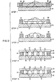
step 1 of Fig. 1 in particular, there is illustrated atypical substrate 10 to which a device can be bonded. Thesubstrate 10 has a set of solderwettable pads 12 mounted on a ceramic base with either an internal metallurgy system that interconnects the pads with pin (not shown), and other associated devices, and/or a metallurgy formed on the top surface. In the interest of clarity only a single set of pads is shown. In practice the substrate can have many sets of pads for a connection to many devices, as shown in U.S. 4,245,273. The metallurgy can be located on the surface, or on the surface and also internally, if desired.Substrate 10 is illustrative of a general type substrate, which substrate structure does not constitute part of the invention. In general, thesubstrate 10 is formed of a ceramic material which normally has a coefficient of expansion that differs from the coefficient of expansion of silicon, the material used to form the semiconductor device to be bonded to the substrate. -
Step 2 shows ablank silicon substrate 14 having bonded theretosolder extenders 16 formed of a suitable solder alloy having a relatively high melting point. Typically the solder extenders will be formed of a pure Pb or a solder with a very high Pb composition. The melting point of the extender should be material of the order of 327°C. On the top surface of each ofextenders 16 is alayer 18 of a low melting metal, typically tin with a thickness in the range of 40 to 60 nm and a melting point on the order of 240°C. Thesolder extenders 16 are formed by placing a suitable apertured mask having apertures corresponding to the pad configuration onsubstrate 10 and vapor depositing the solder alloy on thesubstrate 14 to the appropriate desired depth, typically in the range of 50 to 100 nm. Thelow melting layer 18 is subsequently deposited on the top surfaces of the extenders also by vapor deposition. As indicated instep 3, theblank silicon substrate 14 with theextenders 16 is then inverted and placed on the top surface ofsubstrate 10 with thelayer 18 in contact with the surface ofpad 12. Thesolder extenders 16 are transferred to the substrate by heating the resultant assembly to a temperature sufficient to melt thelayer 18 and subsequently cooling to fuse the extenders to thepads 12. Theblank silicon substrate 14 can then be conveniently removed leaving the structure illustrated instep 4. The integratedcircuit semiconductor device 20 to be bonded tosubstrate 10 is illustrated instep 5.Device 20 has a plurality ofsolder mounds 22 arranged in a configuration to match the configuration ofsolder pads 12 onsubstrate 10. Thesolder terminals 22 each consists of a solderwettable pad structure 21 with a mound of solder reflowed thereto on the top surface. As indicated, the peripheral portion ofdevice 20 extends outwardly beyond thesolder terminals 22.Device 20 is conventional and consists of many active and passive semiconductor elements interconnected with a suitable metallurgy system (not shown). On the peripheral portion ofdevice 20 there is provided solderwettable pads 24 which are normally fabricated along with thepads 21 ondevice 20. Any suitable number of pads can be provided since they form the basis for the means to maintain a predetermined vertical spacing between the semiconductor device and the substrate. In general a minimum of three pads per device structure must be provided although more can be used if desired. The means for maintaining the spacing is fabricated as shown instep 6. Amask 26 havingapertures 28 that overliepads 24 is placed on the top surface ofdevice 20. A thin layer ofsolder 30 is vapor deposited on the top surface ofpads 24 by conventional vapor deposition techniques.Metal spheres 32 having a diameter approximately the desired spacing of the substrate and the device are placed inapertures 28 and the assembly is heated to melt thelayer 30 and subsequently cooled to join the spheres to thedevice 20. The metal spheres can be any suitable metal but are preferably formed of copper with a nickel coating on the surface with an overlying coating of gold. The spheres will normally have a diameter in the order of 125 µm. After themask 26 is removed the assembly is inverted and placed into position onsubstrate 10 havingextenders 16 on the pads as shown instep 7. As illustrated thespheres 32 provide standoffs that maintain the desired spacing between the device and the substrate, and each I/O pad on the device is connected to a corresponding pad on the substrate with each solder mound in contact with a solder extender. The assembly is then heated to a temperature sufficient to melt the material of theextender 16 and thesolder mound 22 thus forming elongated hour-glass shapedsolder connections 38 between the pads on the device and the substrate. The total amount of solder in theextenders 16 and thesolder mound 22 is calculated, considering the spacing between pads to provide the hour-glass shaped connections. - Referring now the Fig. 2 of the drawings there is depicted a second sequence of steps illustrating a second preferred embodiment of the process of our invention. In this embodiment the
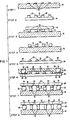
substrate 10 can be any suitable support for a semiconductor device as discussed previously in the description of the first preferred embodiment.Substrate 10 can also be an unsintered ceramic substrate, as for example a MLC substrate. Amask 40 withopenings 42 is positioned on the top surface ofsubstrate 10 withopenings 42 positioned over the desired locations of the standoff to be fabricated. A metal paste consisting of a particulate metal, preferably refractory material such as molybdenum, tantalum or tungsten combined with a suitable vehicle is screened intoopenings 42 formingstandoff elements 44. Following thescreening operation mask 40 is removed and the assembly sintered thereby driving off the vehicle plasticizers, etc. in the paste and also the binders in the greenceramic substrate 10 if the substrate has not been previously sintered. The height of thestandoff 44 after sintering corresponds to the desired spacing between the device to be positioned on the substrate and thesubstrate 10. Any shrinkage due to sintering must be accommodated by increasing the thickness ofmask 40. Thesolder extenders 16 shown in Fig. 2 adhered toblank substrate 14 are fabricated in the same manner described in the previous embodiment. Theblank substrate 14 is positioned over thepads 12 and heated to fuse theextenders 16 to the pads and theblank substrate 14 is subsequently removed leaving the structure shown instep 3. As shown instep 4, a semiconductor device provided withsolder mounds 22 is positioned over the substrate with the solder mounds in contact with thesolder extenders 16 and the peripheral portion of the device in abutting contact with thestandoff elements 44. The assembly is then heated to reflow the solder element resulting in the structure illustrated instep 5 wherein thesolder connections 38 are elongated and have an hour-glass figure. - Obvious modifications can be made to the process embodiment described as for example the spherical standoffs that were adhered to the substrate in the
first embodiment 10 could instead be adhered to pads mounted on thesubstrate 10 if desired. Further the location of the standoffs either on the device or the substrate can be varied to suit the individual application. Further the standoffs themselves can be used as an I/0 or ground terminal provided that the necessary connections are made in the substrate and the semiconductor device. - While the invention has been illustrated and described with reference to preferred embodiments thereof, it is to be understood that the invention is not limited to the precise construction herein disclosed and the right is reserved to all changes and modifications coming within the scope of the invention as defined in the appended claims.
Claims (11)
Applications Claiming Priority (2)
| Application Number | Priority Date | Filing Date | Title |
|---|---|---|---|
| US06/555,264 US4545610A (en) | 1983-11-25 | 1983-11-25 | Method for forming elongated solder connections between a semiconductor device and a supporting substrate |
| US555264 | 1995-11-08 |
Publications (2)
| Publication Number | Publication Date |
|---|---|
| EP0147576A1 EP0147576A1 (en) | 1985-07-10 |
| EP0147576B1 true EP0147576B1 (en) | 1989-06-14 |
Family
ID=24216611
Family Applications (1)
| Application Number | Title | Priority Date | Filing Date |
|---|---|---|---|
| EP84113328A Expired EP0147576B1 (en) | 1983-11-25 | 1984-11-06 | Process for forming elongated solder connections between a semiconductor device and a supporting substrate |
Country Status (4)
| Country | Link |
|---|---|
| US (1) | US4545610A (en) |
| EP (1) | EP0147576B1 (en) |
| JP (1) | JPS60119737A (en) |
| DE (1) | DE3478729D1 (en) |
Families Citing this family (229)
| Publication number | Priority date | Publication date | Assignee | Title |
|---|---|---|---|---|
| US4604644A (en) * | 1985-01-28 | 1986-08-05 | International Business Machines Corporation | Solder interconnection structure for joining semiconductor devices to substrates that have improved fatigue life, and process for making |
| US4661375A (en) * | 1985-04-22 | 1987-04-28 | At&T Technologies, Inc. | Method for increasing the height of solder bumps |
| JPS61260648A (en) * | 1985-05-15 | 1986-11-18 | Matsushita Electric Ind Co Ltd | Packaging method for semiconductor device |
| JPS629642A (en) * | 1985-07-05 | 1987-01-17 | Matsushita Electric Ind Co Ltd | Manufacture of semiconductor device |
| GB8522429D0 (en) * | 1985-09-10 | 1985-10-16 | Plessey Co Plc | Alignment for hybrid device |
| US5476211A (en) * | 1993-11-16 | 1995-12-19 | Form Factor, Inc. | Method of manufacturing electrical contacts, using a sacrificial member |
| US5917707A (en) | 1993-11-16 | 1999-06-29 | Formfactor, Inc. | Flexible contact structure with an electrically conductive shell |
| US4695861A (en) * | 1985-10-21 | 1987-09-22 | Honeywell Inc. | Backside mosaic photoconductive infrared detector array |
| JPS6284973U (en) * | 1985-11-19 | 1987-05-30 | ||
| US4807021A (en) * | 1986-03-10 | 1989-02-21 | Kabushiki Kaisha Toshiba | Semiconductor device having stacking structure |
| EP0248566A3 (en) * | 1986-05-30 | 1990-01-31 | AT&T Corp. | Process for controlling solder joint geometry when surface mounting a leadless integrated circuit package on a substrate |
| GB2194387A (en) * | 1986-08-20 | 1988-03-02 | Plessey Co Plc | Bonding integrated circuit devices |
| DE3785720T2 (en) * | 1986-09-25 | 1993-08-12 | Toshiba Kawasaki Kk | METHOD FOR PRODUCING A FILM CARRIER. |
| DE3788263T2 (en) * | 1986-09-25 | 1994-03-24 | Toshiba Kawasaki Kk | Method for electrically connecting two objects. |
| US4760948A (en) * | 1986-12-23 | 1988-08-02 | Rca Corporation | Leadless chip carrier assembly and method |
| US5170931A (en) * | 1987-03-11 | 1992-12-15 | International Business Machines Corporation | Method and apparatus for mounting a flexible film semiconductor chip carrier on a circuitized substrate |
| US4845542A (en) * | 1987-03-19 | 1989-07-04 | Unisys Corporation | Interconnect for layered integrated circuit assembly |
| US4831724A (en) * | 1987-08-04 | 1989-05-23 | Western Digital Corporation | Apparatus and method for aligning surface mountable electronic components on printed circuit board pads |
| US4912545A (en) * | 1987-09-16 | 1990-03-27 | Irvine Sensors Corporation | Bonding of aligned conductive bumps on adjacent surfaces |
| US4803450A (en) * | 1987-12-14 | 1989-02-07 | General Electric Company | Multilayer circuit board fabricated from silicon |
| US4980753A (en) * | 1988-11-21 | 1990-12-25 | Honeywell Inc. | Low-cost high-performance semiconductor chip package |
| US5208186A (en) * | 1989-02-09 | 1993-05-04 | National Semiconductor Corporation | Process for reflow bonding of bumps in IC devices |
| US4935627A (en) * | 1989-03-13 | 1990-06-19 | Honeywell Inc. | Electrical interconnection apparatus for achieving precise alignment of hybrid components |
| GB2236217A (en) * | 1989-08-23 | 1991-03-27 | Itt Ind Ltd | Improvement relating to electrical connectors |
| US5489804A (en) * | 1989-08-28 | 1996-02-06 | Lsi Logic Corporation | Flexible preformed planar structures for interposing between a chip and a substrate |
| US5834799A (en) * | 1989-08-28 | 1998-11-10 | Lsi Logic | Optically transmissive preformed planar structures |
| JP2805245B2 (en) * | 1989-08-28 | 1998-09-30 | エルエスアイ ロジック コーポレーション | Flip chip structure |
| US5299730A (en) * | 1989-08-28 | 1994-04-05 | Lsi Logic Corporation | Method and apparatus for isolation of flux materials in flip-chip manufacturing |
| US5168346A (en) * | 1989-08-28 | 1992-12-01 | Lsi Logic Corporation | Method and apparatus for isolation of flux materials in flip-chip manufacturing |
| US5504035A (en) * | 1989-08-28 | 1996-04-02 | Lsi Logic Corporation | Process for solder ball interconnecting a semiconductor device to a substrate using a noble metal foil embedded interposer substrate |
| US5175612A (en) * | 1989-12-19 | 1992-12-29 | Lsi Logic Corporation | Heat sink for semiconductor device assembly |
| CA2034703A1 (en) * | 1990-01-23 | 1991-07-24 | Masanori Nishiguchi | Substrate for packaging a semiconductor device |
| US5056216A (en) * | 1990-01-26 | 1991-10-15 | Sri International | Method of forming a plurality of solder connections |
| US6471115B1 (en) | 1990-02-19 | 2002-10-29 | Hitachi, Ltd. | Process for manufacturing electronic circuit devices |
| US6227436B1 (en) | 1990-02-19 | 2001-05-08 | Hitachi, Ltd. | Method of fabricating an electronic circuit device and apparatus for performing the method |
| US5130779A (en) * | 1990-06-19 | 1992-07-14 | International Business Machines Corporation | Solder mass having conductive encapsulating arrangement |
| US5251806A (en) * | 1990-06-19 | 1993-10-12 | International Business Machines Corporation | Method of forming dual height solder interconnections |
| US5060844A (en) * | 1990-07-18 | 1991-10-29 | International Business Machines Corporation | Interconnection structure and test method |
| US5011066A (en) * | 1990-07-27 | 1991-04-30 | Motorola, Inc. | Enhanced collapse solder interconnection |
| ZA915965B (en) * | 1990-07-30 | 1992-04-29 | South Africa Ind Dev Corp | Attaching integrated circuits to circuit boards |
| US5399903A (en) * | 1990-08-15 | 1995-03-21 | Lsi Logic Corporation | Semiconductor device having an universal die size inner lead layout |
| FR2666173A1 (en) * | 1990-08-21 | 1992-02-28 | Thomson Csf | HYBRID INTERCONNECTION STRUCTURE FOR INTEGRATED CIRCUITS AND MANUFACTURING METHOD. |
| US5057969A (en) * | 1990-09-07 | 1991-10-15 | International Business Machines Corporation | Thin film electronic device |
| US5148265A (en) | 1990-09-24 | 1992-09-15 | Ist Associates, Inc. | Semiconductor chip assemblies with fan-in leads |
| US5679977A (en) * | 1990-09-24 | 1997-10-21 | Tessera, Inc. | Semiconductor chip assemblies, methods of making same and components for same |
| US5258330A (en) * | 1990-09-24 | 1993-11-02 | Tessera, Inc. | Semiconductor chip assemblies with fan-in leads |
| US7198969B1 (en) | 1990-09-24 | 2007-04-03 | Tessera, Inc. | Semiconductor chip assemblies, methods of making same and components for same |
| US5148266A (en) * | 1990-09-24 | 1992-09-15 | Ist Associates, Inc. | Semiconductor chip assemblies having interposer and flexible lead |
| JPH04170811A (en) * | 1990-11-05 | 1992-06-18 | Fujitsu Ltd | Surface acoustic wave device |
| US5154341A (en) * | 1990-12-06 | 1992-10-13 | Motorola Inc. | Noncollapsing multisolder interconnection |
| US5233504A (en) * | 1990-12-06 | 1993-08-03 | Motorola, Inc. | Noncollapsing multisolder interconnection |
| US5220200A (en) * | 1990-12-10 | 1993-06-15 | Delco Electronics Corporation | Provision of substrate pillars to maintain chip standoff |
| US5157480A (en) * | 1991-02-06 | 1992-10-20 | Motorola, Inc. | Semiconductor device having dual electrical contact sites |
| US5266520A (en) * | 1991-02-11 | 1993-11-30 | International Business Machines Corporation | Electronic packaging with varying height connectors |
| US5148968A (en) * | 1991-02-11 | 1992-09-22 | Motorola, Inc. | Solder bump stretch device |
| KR920022482A (en) * | 1991-05-09 | 1992-12-19 | 가나이 쯔도무 | Electronic component mounting module |
| US5160409A (en) * | 1991-08-05 | 1992-11-03 | Motorola, Inc. | Solder plate reflow method for forming a solder bump on a circuit trace intersection |
| US5194137A (en) * | 1991-08-05 | 1993-03-16 | Motorola Inc. | Solder plate reflow method for forming solder-bumped terminals |
| US5133495A (en) * | 1991-08-12 | 1992-07-28 | International Business Machines Corporation | Method of bonding flexible circuit to circuitized substrate to provide electrical connection therebetween |
| US5203075A (en) * | 1991-08-12 | 1993-04-20 | Inernational Business Machines | Method of bonding flexible circuit to cicuitized substrate to provide electrical connection therebetween using different solders |
| US5249098A (en) * | 1991-08-22 | 1993-09-28 | Lsi Logic Corporation | Semiconductor device package with solder bump electrical connections on an external surface of the package |
| JP2555811B2 (en) * | 1991-09-10 | 1996-11-20 | 富士通株式会社 | Flip chip bonding method for semiconductor chips |
| CA2077161A1 (en) * | 1991-09-13 | 1993-03-14 | Thomas W. Fitzgerald | Method of establishing soldered connections |
| US5186383A (en) * | 1991-10-02 | 1993-02-16 | Motorola, Inc. | Method for forming solder bump interconnections to a solder-plated circuit trace |
| DE69331876T2 (en) * | 1992-01-28 | 2002-11-28 | British Telecommunications P.L.C., London | Alignment of integrated optical components |
| US5338208A (en) * | 1992-02-04 | 1994-08-16 | International Business Machines Corporation | High density electronic connector and method of assembly |
| US5434750A (en) * | 1992-02-07 | 1995-07-18 | Lsi Logic Corporation | Partially-molded, PCB chip carrier package for certain non-square die shapes |
| WO1993019487A1 (en) * | 1992-03-24 | 1993-09-30 | Unisys Corporation | Integrated circuit module having microscopic self-alignment features |
| US5269453A (en) * | 1992-04-02 | 1993-12-14 | Motorola, Inc. | Low temperature method for forming solder bump interconnections to a plated circuit trace |
| US5324892A (en) * | 1992-08-07 | 1994-06-28 | International Business Machines Corporation | Method of fabricating an electronic interconnection |
| US5334804A (en) * | 1992-11-17 | 1994-08-02 | Fujitsu Limited | Wire interconnect structures for connecting an integrated circuit to a substrate |
| JP2716336B2 (en) * | 1993-03-10 | 1998-02-18 | 日本電気株式会社 | Integrated circuit device |
| US5329423A (en) * | 1993-04-13 | 1994-07-12 | Scholz Kenneth D | Compressive bump-and-socket interconnection scheme for integrated circuits |
| US5767580A (en) * | 1993-04-30 | 1998-06-16 | Lsi Logic Corporation | Systems having shaped, self-aligning micro-bump structures |
| US5616206A (en) * | 1993-06-15 | 1997-04-01 | Ricoh Company, Ltd. | Method for arranging conductive particles on electrodes of substrate |
| US5438477A (en) * | 1993-08-12 | 1995-08-01 | Lsi Logic Corporation | Die-attach technique for flip-chip style mounting of semiconductor dies |
| JP3194553B2 (en) * | 1993-08-13 | 2001-07-30 | 富士通株式会社 | Method for manufacturing semiconductor device |
| US5388327A (en) * | 1993-09-15 | 1995-02-14 | Lsi Logic Corporation | Fabrication of a dissolvable film carrier containing conductive bump contacts for placement on a semiconductor device package |
| US5591941A (en) * | 1993-10-28 | 1997-01-07 | International Business Machines Corporation | Solder ball interconnected assembly |
| US7084656B1 (en) | 1993-11-16 | 2006-08-01 | Formfactor, Inc. | Probe for semiconductor devices |
| US20020053734A1 (en) | 1993-11-16 | 2002-05-09 | Formfactor, Inc. | Probe card assembly and kit, and methods of making same |
| US7073254B2 (en) * | 1993-11-16 | 2006-07-11 | Formfactor, Inc. | Method for mounting a plurality of spring contact elements |
| US5820014A (en) | 1993-11-16 | 1998-10-13 | Form Factor, Inc. | Solder preforms |
| US7200930B2 (en) | 1994-11-15 | 2007-04-10 | Formfactor, Inc. | Probe for semiconductor devices |
| US5471011A (en) * | 1994-05-26 | 1995-11-28 | Ak Technology, Inc. | Homogeneous thermoplastic semi-conductor chip carrier package |
| US5466635A (en) * | 1994-06-02 | 1995-11-14 | Lsi Logic Corporation | Process for making an interconnect bump for flip-chip integrated circuit including integral standoff and hourglass shaped solder coating |
| US5700715A (en) * | 1994-06-14 | 1997-12-23 | Lsi Logic Corporation | Process for mounting a semiconductor device to a circuit substrate |
| US5657206A (en) * | 1994-06-23 | 1997-08-12 | Cubic Memory, Inc. | Conductive epoxy flip-chip package and method |
| US6486003B1 (en) * | 1996-12-13 | 2002-11-26 | Tessera, Inc. | Expandable interposer for a microelectronic package and method therefor |
| US6848173B2 (en) | 1994-07-07 | 2005-02-01 | Tessera, Inc. | Microelectric packages having deformed bonded leads and methods therefor |
| US5539153A (en) * | 1994-08-08 | 1996-07-23 | Hewlett-Packard Company | Method of bumping substrates by contained paste deposition |
| US5567648A (en) * | 1994-08-29 | 1996-10-22 | Motorola, Inc. | Process for providing interconnect bumps on a bonding pad by application of a sheet of conductive discs |
| US5542174A (en) * | 1994-09-15 | 1996-08-06 | Intel Corporation | Method and apparatus for forming solder balls and solder columns |
| US5915170A (en) * | 1994-09-20 | 1999-06-22 | Tessera, Inc. | Multiple part compliant interface for packaging of a semiconductor chip and method therefor |
| US5665989A (en) * | 1995-01-03 | 1997-09-09 | Lsi Logic | Programmable microsystems in silicon |
| US5726861A (en) * | 1995-01-03 | 1998-03-10 | Ostrem; Fred E. | Surface mount component height control |
| US5573171A (en) * | 1995-02-16 | 1996-11-12 | Trw Inc. | Method of thin film patterning by reflow |
| US6388203B1 (en) | 1995-04-04 | 2002-05-14 | Unitive International Limited | Controlled-shaped solder reservoirs for increasing the volume of solder bumps, and structures formed thereby |
| DE69628161T2 (en) | 1995-04-05 | 2004-03-25 | Unitive International Ltd. | A SOLDERING STRUCTURE FOR A MICROELECTRONIC SUBSTRATE |
| US5874782A (en) * | 1995-08-24 | 1999-02-23 | International Business Machines Corporation | Wafer with elevated contact structures |
| US5770889A (en) * | 1995-12-29 | 1998-06-23 | Lsi Logic Corporation | Systems having advanced pre-formed planar structures |
| US5994152A (en) | 1996-02-21 | 1999-11-30 | Formfactor, Inc. | Fabricating interconnects and tips using sacrificial substrates |
| US8033838B2 (en) | 1996-02-21 | 2011-10-11 | Formfactor, Inc. | Microelectronic contact structure |
| US6030856A (en) * | 1996-06-10 | 2000-02-29 | Tessera, Inc. | Bondable compliant pads for packaging of a semiconductor chip and method therefor |
| US6395991B1 (en) * | 1996-07-29 | 2002-05-28 | International Business Machines Corporation | Column grid array substrate attachment with heat sink stress relief |
| JPH1070153A (en) * | 1996-08-26 | 1998-03-10 | Hitachi Ltd | Method for connecting electronic component |
| US5829668A (en) * | 1996-09-03 | 1998-11-03 | Motorola Corporation | Method for forming solder bumps on bond pads |
| JP3553300B2 (en) * | 1996-12-02 | 2004-08-11 | 富士通株式会社 | Semiconductor device manufacturing method and semiconductor device mounting method |
| US5937276A (en) | 1996-12-13 | 1999-08-10 | Tessera, Inc. | Bonding lead structure with enhanced encapsulation |
| US6686015B2 (en) | 1996-12-13 | 2004-02-03 | Tessera, Inc. | Transferable resilient element for packaging of a semiconductor chip and method therefor |
| US5957370A (en) * | 1997-01-10 | 1999-09-28 | Integrated Device Technology, Inc. | Plating process for fine pitch die in wafer form |
| US6330967B1 (en) | 1997-03-13 | 2001-12-18 | International Business Machines Corporation | Process to produce a high temperature interconnection |
| US5859474A (en) * | 1997-04-23 | 1999-01-12 | Lsi Logic Corporation | Reflow ball grid array assembly |
| US7842599B2 (en) * | 1997-05-27 | 2010-11-30 | Wstp, Llc | Bumping electronic components using transfer substrates |
| US6293456B1 (en) | 1997-05-27 | 2001-09-25 | Spheretek, Llc | Methods for forming solder balls on substrates |
| US7007833B2 (en) | 1997-05-27 | 2006-03-07 | Mackay John | Forming solder balls on substrates |
| US7654432B2 (en) | 1997-05-27 | 2010-02-02 | Wstp, Llc | Forming solder balls on substrates |
| US7288471B2 (en) * | 1997-05-27 | 2007-10-30 | Mackay John | Bumping electronic components using transfer substrates |
| US7819301B2 (en) * | 1997-05-27 | 2010-10-26 | Wstp, Llc | Bumping electronic components using transfer substrates |
| US6609652B2 (en) | 1997-05-27 | 2003-08-26 | Spheretek, Llc | Ball bumping substrates, particuarly wafers |
| US6195268B1 (en) * | 1997-06-09 | 2001-02-27 | Floyd K. Eide | Stacking layers containing enclosed IC chips |
| US6096576A (en) | 1997-09-02 | 2000-08-01 | Silicon Light Machines | Method of producing an electrical interface to an integrated circuit device having high density I/O count |
| US6335222B1 (en) * | 1997-09-18 | 2002-01-01 | Tessera, Inc. | Microelectronic packages with solder interconnections |
| US6324069B1 (en) * | 1997-10-29 | 2001-11-27 | Hestia Technologies, Inc. | Chip package with molded underfill |
| US6495083B2 (en) | 1997-10-29 | 2002-12-17 | Hestia Technologies, Inc. | Method of underfilling an integrated circuit chip |
| US5984164A (en) * | 1997-10-31 | 1999-11-16 | Micron Technology, Inc. | Method of using an electrically conductive elevation shaping tool |
| US6059173A (en) | 1998-03-05 | 2000-05-09 | International Business Machines Corporation | Micro grid array solder interconnection structure for second level packaging joining a module and printed circuit board |
| US5923955A (en) * | 1998-05-28 | 1999-07-13 | Xerox Corporation | Fine flip chip interconnection |
| US6070782A (en) * | 1998-07-09 | 2000-06-06 | International Business Machines Corporation | Socketable bump grid array shaped-solder on copper spheres |
| US6303986B1 (en) | 1998-07-29 | 2001-10-16 | Silicon Light Machines | Method of and apparatus for sealing an hermetic lid to a semiconductor die |
| US6713238B1 (en) | 1998-10-09 | 2004-03-30 | Stephen Y. Chou | Microscale patterning and articles formed thereby |
| AU1444800A (en) * | 1998-10-09 | 2000-05-01 | Trustees Of Princeton University, The | Microscale patterning and articles formed thereby |
| US6177729B1 (en) | 1999-04-03 | 2001-01-23 | International Business Machines Corporation | Rolling ball connector |
| SE523164C2 (en) * | 1999-05-17 | 2004-03-30 | Ericsson Telefon Ab L M | Mounting arrangement for semiconductor elements with solder beads for alignment to receiving surface |
| US6274474B1 (en) | 1999-10-25 | 2001-08-14 | International Business Machines Corporation | Method of forming BGA interconnections having mixed solder profiles |
| US6410861B1 (en) * | 1999-12-03 | 2002-06-25 | Motorola, Inc. | Low profile interconnect structure |
| US6956878B1 (en) | 2000-02-07 | 2005-10-18 | Silicon Light Machines Corporation | Method and apparatus for reducing laser speckle using polarization averaging |
| EP1332654B1 (en) | 2000-11-10 | 2005-01-12 | Unitive Electronics, Inc. | Methods of positioning components using liquid prime movers and related structures |
| US6863209B2 (en) | 2000-12-15 | 2005-03-08 | Unitivie International Limited | Low temperature methods of bonding components |
| US6707591B2 (en) | 2001-04-10 | 2004-03-16 | Silicon Light Machines | Angled illumination for a single order light modulator based projection system |
| US20030087477A1 (en) * | 2001-05-02 | 2003-05-08 | Tomohiro Kawashima | Repairable flip clip semiconductor device with excellent packaging reliability and method of manufacturing same |
| KR100443504B1 (en) * | 2001-06-12 | 2004-08-09 | 주식회사 하이닉스반도체 | ball grid array package and method of fabricating the same |
| US6683375B2 (en) * | 2001-06-15 | 2004-01-27 | Fairchild Semiconductor Corporation | Semiconductor die including conductive columns |
| US6782205B2 (en) | 2001-06-25 | 2004-08-24 | Silicon Light Machines | Method and apparatus for dynamic equalization in wavelength division multiplexing |
| US6747781B2 (en) | 2001-06-25 | 2004-06-08 | Silicon Light Machines, Inc. | Method, apparatus, and diffuser for reducing laser speckle |
| US6829092B2 (en) | 2001-08-15 | 2004-12-07 | Silicon Light Machines, Inc. | Blazed grating light valve |
| US6541710B1 (en) * | 2001-11-16 | 2003-04-01 | Hewlett-Packard Company | Method and apparatus of supporting circuit component having a solder column array using interspersed rigid columns |
| US6809937B2 (en) * | 2001-11-16 | 2004-10-26 | Hewlett-Packard Development Company, L.P. | Method and apparatus for shock and vibration isolation of a circuit component |
| US6813162B2 (en) * | 2001-11-16 | 2004-11-02 | Hewlett-Packard Development Company, L.P. | Method and apparatus for supporting circuit component having solder column array interconnects using interposed support shims |
| US6710264B2 (en) | 2001-11-16 | 2004-03-23 | Hewlett-Packard Development Company, L.P. | Method and apparatus for supporting a circuit component having solder column interconnects using external support |
| US6800238B1 (en) | 2002-01-15 | 2004-10-05 | Silicon Light Machines, Inc. | Method for domain patterning in low coercive field ferroelectrics |
| US6908845B2 (en) * | 2002-03-28 | 2005-06-21 | Intel Corporation | Integrated circuit die and an electronic assembly having a three-dimensional interconnection scheme |
| US6848177B2 (en) * | 2002-03-28 | 2005-02-01 | Intel Corporation | Integrated circuit die and an electronic assembly having a three-dimensional interconnection scheme |
| US20030183943A1 (en) * | 2002-03-28 | 2003-10-02 | Swan Johanna M. | Integrated circuit die and an electronic assembly having a three-dimensional interconnection scheme |
| US6600661B1 (en) | 2002-04-08 | 2003-07-29 | Hewlett-Packard Development Company, L.P. | Method and apparatus for supporting a circuit component |
| US6728023B1 (en) | 2002-05-28 | 2004-04-27 | Silicon Light Machines | Optical device arrays with optimized image resolution |
| US6767751B2 (en) | 2002-05-28 | 2004-07-27 | Silicon Light Machines, Inc. | Integrated driver process flow |
| US6822797B1 (en) | 2002-05-31 | 2004-11-23 | Silicon Light Machines, Inc. | Light modulator structure for producing high-contrast operation using zero-order light |
| US7547623B2 (en) | 2002-06-25 | 2009-06-16 | Unitive International Limited | Methods of forming lead free solder bumps |
| WO2004001837A2 (en) | 2002-06-25 | 2003-12-31 | Unitive International Limited | Methods of forming electronic structures including conductive shunt layers and related structures |
| US7531898B2 (en) | 2002-06-25 | 2009-05-12 | Unitive International Limited | Non-Circular via holes for bumping pads and related structures |
| US6829258B1 (en) | 2002-06-26 | 2004-12-07 | Silicon Light Machines, Inc. | Rapidly tunable external cavity laser |
| US6714337B1 (en) | 2002-06-28 | 2004-03-30 | Silicon Light Machines | Method and device for modulating a light beam and having an improved gamma response |
| US6813059B2 (en) | 2002-06-28 | 2004-11-02 | Silicon Light Machines, Inc. | Reduced formation of asperities in contact micro-structures |
| US6801354B1 (en) | 2002-08-20 | 2004-10-05 | Silicon Light Machines, Inc. | 2-D diffraction grating for substantially eliminating polarization dependent losses |
| US6712480B1 (en) | 2002-09-27 | 2004-03-30 | Silicon Light Machines | Controlled curvature of stressed micro-structures |
| US6987600B1 (en) | 2002-12-17 | 2006-01-17 | Silicon Light Machines Corporation | Arbitrary phase profile for better equalization in dynamic gain equalizer |
| US6953956B2 (en) * | 2002-12-18 | 2005-10-11 | Easic Corporation | Semiconductor device having borderless logic array and flexible I/O |
| US20040147169A1 (en) | 2003-01-28 | 2004-07-29 | Allison Jeffrey W. | Power connector with safety feature |
| TWI225899B (en) | 2003-02-18 | 2005-01-01 | Unitive Semiconductor Taiwan C | Etching solution and method for manufacturing conductive bump using the etching solution to selectively remove barrier layer |
| US6806997B1 (en) | 2003-02-28 | 2004-10-19 | Silicon Light Machines, Inc. | Patterned diffractive light modulator ribbon for PDL reduction |
| US6829077B1 (en) | 2003-02-28 | 2004-12-07 | Silicon Light Machines, Inc. | Diffractive light modulator with dynamically rotatable diffraction plane |
| US7239023B2 (en) * | 2003-09-24 | 2007-07-03 | Tai-Saw Technology Co., Ltd. | Package assembly for electronic device |
| US7049216B2 (en) * | 2003-10-14 | 2006-05-23 | Unitive International Limited | Methods of providing solder structures for out plane connections |
| US6890795B1 (en) * | 2003-12-30 | 2005-05-10 | Agency For Science, Technology And Research | Wafer level super stretch solder |
| EP1702389B1 (en) | 2003-12-31 | 2020-12-09 | Amphenol FCI Asia Pte. Ltd. | Electrical power contacts and connectors comprising same |
| US7458839B2 (en) | 2006-02-21 | 2008-12-02 | Fci Americas Technology, Inc. | Electrical connectors having power contacts with alignment and/or restraining features |
| US7095105B2 (en) * | 2004-03-23 | 2006-08-22 | Texas Instruments Incorporated | Vertically stacked semiconductor device |
| US7358174B2 (en) | 2004-04-13 | 2008-04-15 | Amkor Technology, Inc. | Methods of forming solder bumps on exposed metal pads |
| US7214104B2 (en) | 2004-09-14 | 2007-05-08 | Fci Americas Technology, Inc. | Ball grid array connector |
| US7476108B2 (en) | 2004-12-22 | 2009-01-13 | Fci Americas Technology, Inc. | Electrical power connectors with cooling features |
| US7226296B2 (en) * | 2004-12-23 | 2007-06-05 | Fci Americas Technology, Inc. | Ball grid array contacts with spring action |
| US7384289B2 (en) | 2005-01-31 | 2008-06-10 | Fci Americas Technology, Inc. | Surface-mount connector |
| US7303427B2 (en) | 2005-04-05 | 2007-12-04 | Fci Americas Technology, Inc. | Electrical connector with air-circulation features |
| US7160757B2 (en) * | 2005-04-25 | 2007-01-09 | Intel Corporation | Gap control between interposer and substrate in electronic assemblies |
| US20070040565A1 (en) * | 2005-08-19 | 2007-02-22 | National University of Singapore, Agency For Science, Technology and Research | Compliant probes and test methodology for fine pitch wafer level devices and interconnects |
| US7745301B2 (en) * | 2005-08-22 | 2010-06-29 | Terapede, Llc | Methods and apparatus for high-density chip connectivity |
| US8957511B2 (en) * | 2005-08-22 | 2015-02-17 | Madhukar B. Vora | Apparatus and methods for high-density chip connectivity |
| US20070045807A1 (en) * | 2005-09-01 | 2007-03-01 | Micron Technology, Inc. | Microelectronic devices and methods for manufacturing microelectronic devices |
| US7674701B2 (en) | 2006-02-08 | 2010-03-09 | Amkor Technology, Inc. | Methods of forming metal layers using multi-layer lift-off patterns |
| US7932615B2 (en) | 2006-02-08 | 2011-04-26 | Amkor Technology, Inc. | Electronic devices including solder bumps on compliant dielectric layers |
| US20080036100A1 (en) * | 2006-05-17 | 2008-02-14 | Tessera, Inc. | Solder elements with columnar structures and methods of making the same |
| US7425145B2 (en) | 2006-05-26 | 2008-09-16 | Fci Americas Technology, Inc. | Connectors and contacts for transmitting electrical power |
| US7726982B2 (en) | 2006-06-15 | 2010-06-01 | Fci Americas Technology, Inc. | Electrical connectors with air-circulation features |
| TWI346826B (en) * | 2006-10-26 | 2011-08-11 | Taiwan Tft Lcd Ass | Bonding structure and method of fabricating the same |
| US7641500B2 (en) | 2007-04-04 | 2010-01-05 | Fci Americas Technology, Inc. | Power cable connector system |
| US7905731B2 (en) | 2007-05-21 | 2011-03-15 | Fci Americas Technology, Inc. | Electrical connector with stress-distribution features |
| US7762857B2 (en) | 2007-10-01 | 2010-07-27 | Fci Americas Technology, Inc. | Power connectors with contact-retention features |
| US8062051B2 (en) | 2008-07-29 | 2011-11-22 | Fci Americas Technology Llc | Electrical communication system having latching and strain relief features |
| USD664096S1 (en) | 2009-01-16 | 2012-07-24 | Fci Americas Technology Llc | Vertical electrical connector |
| USD608293S1 (en) | 2009-01-16 | 2010-01-19 | Fci Americas Technology, Inc. | Vertical electrical connector |
| USD606497S1 (en) | 2009-01-16 | 2009-12-22 | Fci Americas Technology, Inc. | Vertical electrical connector |
| USD640637S1 (en) * | 2009-01-16 | 2011-06-28 | Fci Americas Technology Llc | Vertical electrical connector |
| USD610548S1 (en) | 2009-01-16 | 2010-02-23 | Fci Americas Technology, Inc. | Right-angle electrical connector |
| USD619099S1 (en) | 2009-01-30 | 2010-07-06 | Fci Americas Technology, Inc. | Electrical connector |
| US8323049B2 (en) | 2009-01-30 | 2012-12-04 | Fci Americas Technology Llc | Electrical connector having power contacts |
| US8366485B2 (en) | 2009-03-19 | 2013-02-05 | Fci Americas Technology Llc | Electrical connector having ribbed ground plate |
| USD618180S1 (en) | 2009-04-03 | 2010-06-22 | Fci Americas Technology, Inc. | Asymmetrical electrical connector |
| USD618181S1 (en) | 2009-04-03 | 2010-06-22 | Fci Americas Technology, Inc. | Asymmetrical electrical connector |
| US8296940B2 (en) * | 2010-04-19 | 2012-10-30 | General Electric Company | Method of forming a micro pin hybrid interconnect array |
| KR101712043B1 (en) * | 2010-10-14 | 2017-03-03 | 삼성전자주식회사 | Stacked semiconductor package, Semiconductor device including the stacked semiconductor package and Method of manufacturing the stacked semiconductor package |
| US20120267779A1 (en) | 2011-04-25 | 2012-10-25 | Mediatek Inc. | Semiconductor package |
| US10096540B2 (en) * | 2011-05-13 | 2018-10-09 | STATS ChipPAC Pte. Ltd. | Semiconductor device and method of forming dummy pillars between semiconductor die and substrate for maintaining standoff distance |
| EP2624034A1 (en) | 2012-01-31 | 2013-08-07 | Fci | Dismountable optical coupling device |
| USD727852S1 (en) | 2012-04-13 | 2015-04-28 | Fci Americas Technology Llc | Ground shield for a right angle electrical connector |
| US8944831B2 (en) | 2012-04-13 | 2015-02-03 | Fci Americas Technology Llc | Electrical connector having ribbed ground plate with engagement members |
| USD727268S1 (en) | 2012-04-13 | 2015-04-21 | Fci Americas Technology Llc | Vertical electrical connector |
| US9257778B2 (en) | 2012-04-13 | 2016-02-09 | Fci Americas Technology | High speed electrical connector |
| USD718253S1 (en) | 2012-04-13 | 2014-11-25 | Fci Americas Technology Llc | Electrical cable connector |
| US9543703B2 (en) | 2012-07-11 | 2017-01-10 | Fci Americas Technology Llc | Electrical connector with reduced stack height |
| USD751507S1 (en) | 2012-07-11 | 2016-03-15 | Fci Americas Technology Llc | Electrical connector |
| US8970035B2 (en) | 2012-08-31 | 2015-03-03 | Taiwan Semiconductor Manufacturing Company, Ltd. | Bump structures for semiconductor package |
| US8941236B2 (en) | 2012-09-28 | 2015-01-27 | Intel Corporation | Using collapse limiter structures between elements to reduce solder bump bridging |
| USD745852S1 (en) | 2013-01-25 | 2015-12-22 | Fci Americas Technology Llc | Electrical connector |
| USD720698S1 (en) | 2013-03-15 | 2015-01-06 | Fci Americas Technology Llc | Electrical cable connector |
| US20190206821A1 (en) * | 2017-12-29 | 2019-07-04 | Intel Corporation | Substrate assembly with spacer element |
| TWI736859B (en) * | 2019-03-18 | 2021-08-21 | 矽品精密工業股份有限公司 | Electronic package and manufacturing method thereof |
| DE102021103360A1 (en) * | 2021-02-05 | 2022-08-11 | Few Fahrzeugelektrik Werk Gmbh & Co. Kg | Method of making a pre-tinning assembly and such pre-tinning assembly |
| CN113745169B (en) * | 2021-07-23 | 2023-10-24 | 中国电子科技集团公司第二十九研究所 | Multi-cavity groove LTCC substrate and packaging box welding structure and method |
Family Cites Families (15)
| Publication number | Priority date | Publication date | Assignee | Title |
|---|---|---|---|---|
| US3401126A (en) * | 1965-06-18 | 1968-09-10 | Ibm | Method of rendering noble metal conductive composition non-wettable by solder |
| US3429040A (en) * | 1965-06-18 | 1969-02-25 | Ibm | Method of joining a component to a substrate |
| US3458925A (en) * | 1966-01-20 | 1969-08-05 | Ibm | Method of forming solder mounds on substrates |
| US3486223A (en) * | 1967-04-27 | 1969-12-30 | Philco Ford Corp | Solder bonding |
| US3621565A (en) * | 1969-06-12 | 1971-11-23 | Nasa | Fabrication of single-crystal film semiconductor devices |
| US3871015A (en) * | 1969-08-14 | 1975-03-11 | Ibm | Flip chip module with non-uniform connector joints |
| US3591839A (en) * | 1969-08-27 | 1971-07-06 | Siliconix Inc | Micro-electronic circuit with novel hermetic sealing structure and method of manufacture |
| US3811186A (en) * | 1972-12-11 | 1974-05-21 | Ibm | Method of aligning and attaching circuit devices on a substrate |
| US3997963A (en) * | 1973-06-29 | 1976-12-21 | Ibm Corporation | Novel beam-lead integrated circuit structure and method for making the same including automatic registration of beam-leads with corresponding dielectric substrate leads |
| US3921285A (en) * | 1974-07-15 | 1975-11-25 | Ibm | Method for joining microminiature components to a carrying structure |
| FR2378354A1 (en) * | 1977-01-19 | 1978-08-18 | Alsthom Atlantique | PRESS CONTACT POWER SEMICONDUCTOR MANUFACTURING PROCESS |
| NL7704770A (en) * | 1977-05-02 | 1978-11-06 | Philips Nv | PROCEDURE FOR APPLYING SPACERS TO AN INSULATING SUBSTRATE. |
| JPS5678356U (en) * | 1979-11-12 | 1981-06-25 | ||
| JPS58157146A (en) * | 1982-03-12 | 1983-09-19 | Fujitsu Ltd | Semiconductor device |
| FR2612617B1 (en) * | 1987-03-16 | 1992-07-10 | Bergounhon Rene | OVEN TO DEHYDRATE POWDER, SAND AND AGGREGATES |
-
1983
- 1983-11-25 US US06/555,264 patent/US4545610A/en not_active Expired - Lifetime
-
1984
- 1984-09-20 JP JP59195908A patent/JPS60119737A/en active Granted
- 1984-11-06 DE DE8484113328T patent/DE3478729D1/en not_active Expired
- 1984-11-06 EP EP84113328A patent/EP0147576B1/en not_active Expired
Non-Patent Citations (1)
| Title |
|---|
| IBM TDB, vol. 16, no. 3, August 1973, p. 767 * |
Also Published As
| Publication number | Publication date |
|---|---|
| JPS60119737A (en) | 1985-06-27 |
| EP0147576A1 (en) | 1985-07-10 |
| JPH0263301B2 (en) | 1990-12-27 |
| DE3478729D1 (en) | 1989-07-20 |
| US4545610A (en) | 1985-10-08 |
Similar Documents
| Publication | Publication Date | Title |
|---|---|---|
| EP0147576B1 (en) | Process for forming elongated solder connections between a semiconductor device and a supporting substrate | |
| EP0398485B1 (en) | A method of making a Flip Chip Solder bond structure for devices with gold based metallisation | |
| US6136047A (en) | Solder bump transfer plate | |
| US5698465A (en) | Process for manufacturing an interconnect bump for flip-chip integrated circuit including integral standoff and hourglass shaped solder coating | |
| US5251806A (en) | Method of forming dual height solder interconnections | |
| US5130779A (en) | Solder mass having conductive encapsulating arrangement | |
| KR840000477B1 (en) | Fabrication of circuit packages | |
| US5480835A (en) | Electrical interconnect and method for forming the same | |
| JP3202903B2 (en) | Method of forming solder balls on a substrate | |
| US7449406B2 (en) | Semiconductor element and a producing method for the same, and a semiconductor device and a producing method for the same | |
| US6858941B2 (en) | Multi-chip stack and method of fabrication utilizing self-aligning electrical contact array | |
| EP0473929B1 (en) | Method of forming a thin film electronic device | |
| KR20000053412A (en) | Process for forming cone shaped solder for chip interconnection | |
| JPH098447A (en) | Chip mounting circuit card structure | |
| JPH10256315A (en) | Semiconductor chip bonding pad and its formation | |
| US5198695A (en) | Semiconductor wafer with circuits bonded to a substrate | |
| US5646068A (en) | Solder bump transfer for microelectronics packaging and assembly | |
| US20020076910A1 (en) | High density electronic interconnection | |
| US6258703B1 (en) | Reflow of low melt solder tip C4's | |
| GB2290171A (en) | Inductor chip device | |
| US6179200B1 (en) | Method for forming solder bumps of improved height and devices formed | |
| JP3367826B2 (en) | Semiconductor memory device and method of manufacturing the same | |
| JP3180041B2 (en) | Connection terminal and method of forming the same | |
| JP2741611B2 (en) | Substrate for flip chip bonding | |
| JP3469093B2 (en) | Manufacturing method of printed circuit board and mounted circuit board |
Legal Events
| Date | Code | Title | Description |
|---|---|---|---|
| PUAI | Public reference made under article 153(3) epc to a published international application that has entered the european phase |
Free format text: ORIGINAL CODE: 0009012 |
|
| 17P | Request for examination filed |
Effective date: 19841211 |
|
| AK | Designated contracting states |
Designated state(s): DE FR GB |
|
| 17Q | First examination report despatched |
Effective date: 19871022 |
|
| GRAA | (expected) grant |
Free format text: ORIGINAL CODE: 0009210 |
|
| AK | Designated contracting states |
Kind code of ref document: B1 Designated state(s): DE FR GB |
|
| REF | Corresponds to: |
Ref document number: 3478729 Country of ref document: DE Date of ref document: 19890720 |
|
| ET | Fr: translation filed | ||
| PLBE | No opposition filed within time limit |
Free format text: ORIGINAL CODE: 0009261 |
|
| STAA | Information on the status of an ep patent application or granted ep patent |
Free format text: STATUS: NO OPPOSITION FILED WITHIN TIME LIMIT |
|
| 26N | No opposition filed | ||
| PGFP | Annual fee paid to national office [announced via postgrant information from national office to epo] |
Ref country code: GB Payment date: 19941013 Year of fee payment: 11 |
|
| PGFP | Annual fee paid to national office [announced via postgrant information from national office to epo] |
Ref country code: FR Payment date: 19941103 Year of fee payment: 11 |
|
| PGFP | Annual fee paid to national office [announced via postgrant information from national office to epo] |
Ref country code: DE Payment date: 19941201 Year of fee payment: 11 |
|
| PG25 | Lapsed in a contracting state [announced via postgrant information from national office to epo] |
Ref country code: GB Effective date: 19951106 |
|
| GBPC | Gb: european patent ceased through non-payment of renewal fee |
Effective date: 19951106 |
|
| PG25 | Lapsed in a contracting state [announced via postgrant information from national office to epo] |
Ref country code: FR Effective date: 19960731 |
|
| PG25 | Lapsed in a contracting state [announced via postgrant information from national office to epo] |
Ref country code: DE Effective date: 19960801 |
|
| REG | Reference to a national code |
Ref country code: FR Ref legal event code: ST |