EP0147296A2 - Multiplizierschaltung - Google Patents
Multiplizierschaltung Download PDFInfo
- Publication number
- EP0147296A2 EP0147296A2 EP84402615A EP84402615A EP0147296A2 EP 0147296 A2 EP0147296 A2 EP 0147296A2 EP 84402615 A EP84402615 A EP 84402615A EP 84402615 A EP84402615 A EP 84402615A EP 0147296 A2 EP0147296 A2 EP 0147296A2
- Authority
- EP
- European Patent Office
- Prior art keywords
- carry
- residue
- multiplier
- gates
- res
- Prior art date
- Legal status (The legal status is an assumption and is not a legal conclusion. Google has not performed a legal analysis and makes no representation as to the accuracy of the status listed.)
- Granted
Links
Images


Classifications
-
- G—PHYSICS
- G06—COMPUTING OR CALCULATING; COUNTING
- G06F—ELECTRIC DIGITAL DATA PROCESSING
- G06F7/00—Methods or arrangements for processing data by operating upon the order or content of the data handled
- G06F7/38—Methods or arrangements for performing computations using exclusively denominational number representation, e.g. using binary, ternary, decimal representation
- G06F7/48—Methods or arrangements for performing computations using exclusively denominational number representation, e.g. using binary, ternary, decimal representation using non-contact-making devices, e.g. tube, solid state device; using unspecified devices
- G06F7/52—Multiplying; Dividing
- G06F7/523—Multiplying only
- G06F7/527—Multiplying only in serial-parallel fashion, i.e. one operand being entered serially and the other in parallel
- G06F7/5272—Multiplying only in serial-parallel fashion, i.e. one operand being entered serially and the other in parallel with row wise addition of partial products
- G06F7/5275—Multiplying only in serial-parallel fashion, i.e. one operand being entered serially and the other in parallel with row wise addition of partial products using carry save adders
-
- G—PHYSICS
- G06—COMPUTING OR CALCULATING; COUNTING
- G06F—ELECTRIC DIGITAL DATA PROCESSING
- G06F7/00—Methods or arrangements for processing data by operating upon the order or content of the data handled
-
- G—PHYSICS
- G06—COMPUTING OR CALCULATING; COUNTING
- G06F—ELECTRIC DIGITAL DATA PROCESSING
- G06F11/00—Error detection; Error correction; Monitoring
- G06F11/07—Responding to the occurrence of a fault, e.g. fault tolerance
- G06F11/0703—Error or fault processing not based on redundancy, i.e. by taking additional measures to deal with the error or fault not making use of redundancy in operation, in hardware, or in data representation
- G06F11/0751—Error or fault detection not based on redundancy
- G06F11/0763—Error or fault detection not based on redundancy by bit configuration check, e.g. of formats or tags
-
- G—PHYSICS
- G06—COMPUTING OR CALCULATING; COUNTING
- G06F—ELECTRIC DIGITAL DATA PROCESSING
- G06F7/00—Methods or arrangements for processing data by operating upon the order or content of the data handled
- G06F7/38—Methods or arrangements for performing computations using exclusively denominational number representation, e.g. using binary, ternary, decimal representation
- G06F7/48—Methods or arrangements for performing computations using exclusively denominational number representation, e.g. using binary, ternary, decimal representation using non-contact-making devices, e.g. tube, solid state device; using unspecified devices
- G06F7/52—Multiplying; Dividing
Definitions
- the present invention is related to a multiplication circuit used for a high speed multiplier in a computer system.
- multiplication of binary numbers is performed by repeating addition and carry in the multiplier of the computer system.
- there are two methods of binary number multiplication i.e., one, a parallel arithmetic method using an array circuit arrangement; and two, a carry save adder (CSA) tree method using a plurality of carry save adders, each connected branchwise.
- CSA carry save adder
- the primary object of the present invention is to provide a multiplication circuit used for a high speed multiplier in a computer system.
- Another object of the present invention is to provide a multiplication circuit using carry save adder trees enabling a reduction in the number of gate circuits.
- Still another object of the present invention is a multiplication circuit using carry save adder trees enabling a very precise error check during the operation.
- a multiplication circuit used for a high speed multiplier in a computer system, the multiplication circuit comprising a multiplier and a carry propagating adder, the multiplier obtaining a sum and carry per each bit by using carry save adder trees having a plurality of carry save adders, the multiplier generating a carry generation function and a carry propagating function based on the sum and carry obtained by using a generation/propagation unit, and the carry propagating adder obtaining a final product based on the carry generation function and carry propagation function, according to the present invention, the carry generation function and carry propagation function.generated by the generation/ propagation unit are fed back to a appropriate stage of the carry save adder.
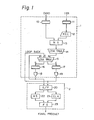
- the multiplication circuit is basically constituted by a multiplier 1 and a carry propagating adder 2.
- the multiplier 1 comprises a resister 10 for setting a multiplicand CAND, a resister 11 for setting a multiplier factor iER, a recoder 12 for setting the iER, a multiple gate 13 for determining a scale factor based on outputs of the resister 10 and the recoder 12, a first stage CSA tree 14 for obtaining the sum and carry based on the output of the multiple gate 13, a final stage CSA tree 15 for obtaining the sum and carry based on the outputs of CSA tree 14 and a loop back of a partial product, a resister 16 for setting the sum S of the partial product from the CSA tree 15, a resister 17 for setting the carry C of the partial product, an output gate 18 for providing a high power output of the sum, and an output gate 19 for providing a high power output of the carry C. Both outputs from the output gates 18 and 19 are fed back to the CSA tree 15 (so-
- the carry propagating adder (CPA) 2 comprises a generation/propagation (G/P) unit 20 for generating a carry generation function and a carry propagation function based on the sum S and the carry C transmitted from the output gates 18 and 19, a carry look ahead logic circuit (CLA) 21, a half sum logic circuit (HS) 22, and a full sum logic circuit (FS) 23 for generating a final product based on the outputs from the G/P unit 20.
- G/P generation/propagation
- CLA carry look ahead logic circuit
- HS half sum logic circuit
- FS full sum logic circuit
- the loop backs of the sum S and the carry C to the CSA tree 15 are performed by the outputs from the gate 18 and 19.
- the structure of the CSA tree 15 is made complex by the use of these loop backs of the sum S and the carry C.
- the multiplier l when the multiplier 1 and the carry propagating adder 2 cannot be incorporated on a single LSI chip, the multiplier l must be provided with high power output gates 18 and 19 because the gates of the resisters 16 and 17 do not provide sufficient power to drive an external terminal.
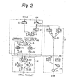
- a conventional error check circuit 3 used in the multiplication circuit is constituted by a residue generator 30 for generating a residue based on the CAND, a residue generator 31 for generating a residue based on the iER, a residue multiplier 32 for multiplying both residues transmitted from both resisters 30 and 31, a residue generator 33 for generating a residue based on the carry C, a residue generator 34 for generating a residue based on the sum S, a residue adder 35 for adding both residues transmitted from both residue generators 33 and 34, and a residue comparator 36 for generating an error ERR based on comparison of a residue obtained by the residue multiplier 32 with a residue obtained by the residue adder 35.
- a conventional error check is performed by comparing the residue obtained from the CAND and the iER with the residue obtained from the sum S and the carry C.
- the structure of the error check circuit is made complex by the use of the residue obtained from the sum S and the carry C.
- a multiplication circuit used for a high speed multiplier in a computer system according to the present invention will now be explained.
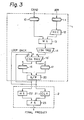
- Fig. 3 the same components as that of Fig. 1 are referred to by the same reference numerals.
- the differences between the conventional multiplication circuit and that of the present invention are first, the loop backs to the CSA tree 15' are changed to the generated term G i and the propagated term P i obtained by the G/P unit 20, and second, the G/P unit 20 is formed in the LSI chip of the multiplier 1 and is directly driven by both resisters 16 and 17, so that both output gates 18 and 19 are eliminated from the multiplier 1.
- the G/P unit 20, .in general, is constituted by a plurality of AND gates and OR gates as shown in Fig. 4, only for an "i"th bit for convenience.
- the relationships between the generated term G. , propagated term P i and the sum S i and the carry C i+1 are shown by the following formulas. where, A i and B i indicate S i and C i+1 , and i indicates a bit number.
- An eight gates type CSA unit UN1 is, in general, constituted by eight AND gates as shown in Fig. 5.
- a, ⁇ , and ⁇ represent inputs to the UN1;
- S and C represent outputs from the CSA unit UN1; and
- minus marks indicate turnover input and turnover output.
- a logic table is as represented by the following table 1.
- a six gates type CSA unit UN2 is constituted by six AND gates as shown in Fig. 6.
- a, G, and P represent inputs looped back from the G/P unit 20 and transmitted from the CSA tree 14.
- S and C represent outputs from the CSA unit.
- a logic table is as represented by the following table 2.
- the CSA tree 14 is constituted by a plurality of UNl's and the CSA tree 15' is constituted by a plurality of UNl's and UN2's.
- UN2 is indicated by the hatched boxes.
- cc indicates the output of the next carry.
- three inputs (G, P and a) transmitted from the G/P unit and the CSA tree 14 are applied to the UN2 in the CSA tree 15'. Accordingly, since one UN2 per nine inputs (i.e.
- Two outputs, i.e., sum S and carry C, obtained by the CSA tree 15' are applied to the G/P unit 20 through the resisters 16 and 17.
- the outputs of the G/P unit 20, i.e., the generated term G i and the propagated term P i are applied to the carry look ahead logic CLA 21 and the half sum logic HS 22 in parallel with the loop back to the CSA tree 15' after conversion to the generated term G and the propagated term P by the G/P unit 20.
- the loop backs to the CSA tree 15' are performed by the generated term G i and the propagated term P. , thereby making it possible to reduce the number of gate circuits in the CS A unit and to improve the operation speed of the multiplication circuit.
- the output gates 18 and 19 are eliminated in the multiplier 1, the G/P unit 20 can function as a high power gate instead of the output gates 18 and 19, because the G/P unit is constituted by the AND gate and the OR gate as explained in Fig. 4.
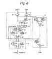
- an error check circuit 4 is constituted by a residue generator 40 for generating a residue based on the CAND, a residue generator 41 for generating a residue based on the iER, a residue multiplier 42 for multiplying both residues transmitted from both residue generators 40 and 41, a residue generator 43 for generating a residue based on the generated term G i and the propagated term P. transmitted from the G/P unit 20, and a residue comparator 44 for generating an error ERR based on comparison of a residue obtained by the residue multiplier 42 with a residue obtained by the residue generator 43.
- an error check according to the present invention is performed by comparing the residues obtained from the CAND and iER with the residues obtained from the generated term G. and propagated term P i .
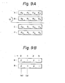
- Figs. 9A and 9B the relationship between inputs A, B and outputs G, P is represented as shown in Fig. 9A by referring to formulas (1) and (2).
- the residue for example, when both inputs A and B are equal to "1" is shown in Fig. 9B.
- there are two residue groups i.e., A and B equal to "2" (a), and A and B equal to "1" (b), at the same bit number.
- the former is in the case of an even bit and the latter is in the case of an odd bit.
- the residue RES (G l ) can be obtained by RES (2) which adds the residue "1" to the residue "1”
- the residue RES (P 1 ) can be obtained by RES (1) which adds the residue "1" to residue "0".
- Table 3 represents the RES when "i" is bit number "0" and the Table 4 represents the RES when "i” is bit number "1".
- X is used for indicating that this number is unnecessary since P 0 and P 1 are always “1” when G 0 and G 1 are “1”, based on formulas (1) and (2).
- the same table as shown in Table 3 is adapted to G 2 and P 2 when "i" is bit number "2”, and the same table as shown in Table 4 is adapted to G 3 and P 3 - when "i" is bit number "3".
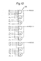
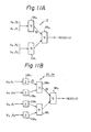
- this gate block GB is used in the residue generator 43 shown in Fig. 8.
- the residue generator 43 in the case of four bits inputs of A and B is constituted by three gate blocks GB 0 to GB 2 , as shown in Fig. 11A.
- the gate block GB is constituted by nine AND gates.
- the residue generator 43 comprises three gates blocks GB 0 to GB 2 shown in Fig. 11A, each of which comprises nine AND gates as shown in Fig. 10. While, the conventional residue generators 33 and 34 comprise three gate blocks GB 0 to GB 2 having nine AND gates per unit and four gate blocks GB 3 to GB 6 having two AND gates per unit shown in Fig. 11B. Two AND gate blocks are used as inputs to each nine AND gate block. Accordingly, in the case of four bits inputs of A and B, conventional residue generators 33 and 34 need thirty five gates (two AND gates X 4, and nine AND gates X 3). While, the residue generator 43 according to the present invention need only twenty seven gates (nine AND gates X 3).
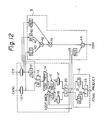
- a detector 50 and a residue multiplier 51 are added to the error check circuit 4 shown in Fig. 8. Moreover, an input to the detector is applied from the iER, and an input to the residue generator 41 is applied from the recoder 12.
- the detector 50 functions as an all "0" detector, i.e., if the iER is all "0", the detector 50 detects this all "0". This all "0" is multiplied by the output of the residue multiplier 42. The following operation is the same as that shown in Fig. 8, and a description thereof is omitted.
Landscapes
- Engineering & Computer Science (AREA)
- Theoretical Computer Science (AREA)
- General Physics & Mathematics (AREA)
- Physics & Mathematics (AREA)
- Mathematical Analysis (AREA)
- Mathematical Optimization (AREA)
- Pure & Applied Mathematics (AREA)
- Computational Mathematics (AREA)
- General Engineering & Computer Science (AREA)
- Computing Systems (AREA)
- Quality & Reliability (AREA)
- Complex Calculations (AREA)
- Error Detection And Correction (AREA)
- Detection And Correction Of Errors (AREA)
Applications Claiming Priority (6)
| Application Number | Priority Date | Filing Date | Title |
|---|---|---|---|
| JP247392/83 | 1983-12-26 | ||
| JP58247392A JPS60136831A (ja) | 1983-12-26 | 1983-12-26 | レシデユ−生成回路 |
| JP25192483A JPH0227686B2 (ja) | 1983-12-27 | 1983-12-27 | Jozankairo |
| JP251924/83 | 1983-12-27 | ||
| JP24135/84 | 1984-02-10 | ||
| JP59024135A JPS60168235A (ja) | 1984-02-10 | 1984-02-10 | 乗算器チエツク方式 |
Publications (3)
| Publication Number | Publication Date |
|---|---|
| EP0147296A2 true EP0147296A2 (de) | 1985-07-03 |
| EP0147296A3 EP0147296A3 (en) | 1988-01-20 |
| EP0147296B1 EP0147296B1 (de) | 1992-03-04 |
Family
ID=27284521
Family Applications (1)
| Application Number | Title | Priority Date | Filing Date |
|---|---|---|---|
| EP84402615A Expired EP0147296B1 (de) | 1983-12-26 | 1984-12-17 | Multiplizierschaltung |
Country Status (8)
| Country | Link |
|---|---|
| US (1) | US4727507A (de) |
| EP (1) | EP0147296B1 (de) |
| KR (1) | KR900000477B1 (de) |
| AU (1) | AU550740B2 (de) |
| BR (1) | BR8406677A (de) |
| CA (1) | CA1232072A (de) |
| DE (1) | DE3485535D1 (de) |
| ES (1) | ES539052A0 (de) |
Families Citing this family (10)
| Publication number | Priority date | Publication date | Assignee | Title |
|---|---|---|---|---|
| JPS6347874A (ja) * | 1986-08-16 | 1988-02-29 | Nec Corp | 算術演算装置 |
| US4989168A (en) * | 1987-11-30 | 1991-01-29 | Fujitsu Limited | Multiplying unit in a computer system, capable of population counting |
| US5283755A (en) * | 1993-04-14 | 1994-02-01 | International Business Machines Corporation | Multiplier employing carry select or carry look-ahead adders in hierarchical tree configuration |
| US5636155A (en) * | 1993-04-27 | 1997-06-03 | Matsushita Electric Industrial Co., Ltd. | Arithmetic processor and arithmetic method |
| US5684731A (en) * | 1995-08-31 | 1997-11-04 | National Semiconductor Corporation | Booth multiplier using data path width adder for efficient carry save addition |
| US5847981A (en) * | 1997-09-04 | 1998-12-08 | Motorola, Inc. | Multiply and accumulate circuit |
| US7543713B2 (en) * | 2001-04-19 | 2009-06-09 | Graham Packaging Company L.P. | Multi-functional base for a plastic, wide-mouth, blow-molded container |
| US6763367B2 (en) * | 2000-12-11 | 2004-07-13 | International Business Machines Corporation | Pre-reduction technique within a multiplier/accumulator architecture |
| US6917956B2 (en) * | 2001-08-14 | 2005-07-12 | Sun Microsystems, Inc. | Apparatus and method for efficient modular exponentiation |
| GB2396708B (en) * | 2002-12-05 | 2006-06-21 | Micron Technology Inc | Hybrid arithmetic logic unit |
Family Cites Families (2)
| Publication number | Priority date | Publication date | Assignee | Title |
|---|---|---|---|---|
| US3840727A (en) * | 1972-10-30 | 1974-10-08 | Amdahl Corp | Binary multiplication by addition with non-verlapping multiplier recording |
| US4041292A (en) * | 1975-12-22 | 1977-08-09 | Honeywell Information Systems Inc. | High speed binary multiplication system employing a plurality of multiple generator circuits |
-
1984
- 1984-12-12 CA CA000469911A patent/CA1232072A/en not_active Expired
- 1984-12-17 DE DE8484402615T patent/DE3485535D1/de not_active Expired - Lifetime
- 1984-12-17 EP EP84402615A patent/EP0147296B1/de not_active Expired
- 1984-12-18 AU AU36856/84A patent/AU550740B2/en not_active Ceased
- 1984-12-21 BR BR8406677A patent/BR8406677A/pt not_active IP Right Cessation
- 1984-12-24 US US06/685,517 patent/US4727507A/en not_active Expired - Fee Related
- 1984-12-24 KR KR8408288A patent/KR900000477B1/ko not_active Expired
- 1984-12-26 ES ES539052A patent/ES539052A0/es active Granted
Non-Patent Citations (2)
| Title |
|---|
| IBM TECHNICAL DISCLOSURE BULLETIN, vol. 10, no. 6, November 1967, pages 727-728, New York, US; R.E. GOLDSCHMIDT: "Dual-mode adder" * |
| PROCEEDINGS OF THE IEEE, vol. 118, nos. 3/4, March/April 1971, pages 499-506, GB; J.B. GOSLING: "Design of large high-speed binary multiplier units" * |
Also Published As
| Publication number | Publication date |
|---|---|
| ES8602271A1 (es) | 1985-11-16 |
| ES539052A0 (es) | 1985-11-16 |
| CA1232072A (en) | 1988-01-26 |
| EP0147296A3 (en) | 1988-01-20 |
| US4727507A (en) | 1988-02-23 |
| BR8406677A (pt) | 1985-10-22 |
| EP0147296B1 (de) | 1992-03-04 |
| KR850004819A (ko) | 1985-07-27 |
| AU550740B2 (en) | 1986-04-10 |
| DE3485535D1 (de) | 1992-04-09 |
| KR900000477B1 (en) | 1990-01-30 |
| AU3685684A (en) | 1985-07-04 |
Similar Documents
| Publication | Publication Date | Title |
|---|---|---|
| Lim | Single-precision multiplier with reduced circuit complexity for signal processing applications | |
| Stenzel et al. | A compact high-speed parallel multiplication scheme | |
| KR940008613B1 (ko) | 캐리선견가산기와 캐리전송방법 | |
| EP0147296A2 (de) | Multiplizierschaltung | |
| US5018093A (en) | High performance self-checking adder having small circuit area | |
| EP1752870B1 (de) | Multiplizierer | |
| Taylor | Compatible hardware for division and square root | |
| US4730266A (en) | Logic full adder circuit | |
| EP0137386A2 (de) | Digitale Multiplizierschaltung | |
| US5177703A (en) | Division circuit using higher radices | |
| JPH0315219B2 (de) | ||
| US6745219B1 (en) | Arithmetic unit using stochastic data processing | |
| US4815019A (en) | Fast ALU equals zero circuit | |
| US5327368A (en) | Chunky binary multiplier and method of operation | |
| US7461107B2 (en) | Converter circuit for converting 1-redundant representation of an integer | |
| EP0326414A2 (de) | Hochgeschwindigkeits-Multiplizierer | |
| JPH0149973B2 (de) | ||
| KR0147942B1 (ko) | 승산기에서의 부스 레코딩회로 | |
| CN215068204U (zh) | 33位加法器、运算电路及芯片 | |
| EP0214836A1 (de) | Addierschaltung mit Auswahl des Übertrags | |
| EP0242600A2 (de) | Verfahren zur Berechnung des Übertragvorgriffs und Schaltung dazu | |
| Lim | High-speed multiplication and multiple summand addition | |
| JPS6083140A (ja) | 乗算器 | |
| EP0213854A2 (de) | Serielle Festkoeffizientmultiplikation und Digitalschaltungen zu deren Ausführung | |
| JPH0673103B2 (ja) | 浮動小数点乗算回路 |
Legal Events
| Date | Code | Title | Description |
|---|---|---|---|
| PUAI | Public reference made under article 153(3) epc to a published international application that has entered the european phase |
Free format text: ORIGINAL CODE: 0009012 |
|
| AK | Designated contracting states |
Designated state(s): DE FR GB |
|
| PUAL | Search report despatched |
Free format text: ORIGINAL CODE: 0009013 |
|
| AK | Designated contracting states |
Kind code of ref document: A3 Designated state(s): DE FR GB |
|
| 17P | Request for examination filed |
Effective date: 19880625 |
|
| 17Q | First examination report despatched |
Effective date: 19891013 |
|
| GRAA | (expected) grant |
Free format text: ORIGINAL CODE: 0009210 |
|
| PGFP | Annual fee paid to national office [announced via postgrant information from national office to epo] |
Ref country code: FR Payment date: 19920210 Year of fee payment: 9 |
|
| AK | Designated contracting states |
Kind code of ref document: B1 Designated state(s): DE FR GB |
|
| REF | Corresponds to: |
Ref document number: 3485535 Country of ref document: DE Date of ref document: 19920409 |
|
| ET | Fr: translation filed | ||
| PGFP | Annual fee paid to national office [announced via postgrant information from national office to epo] |
Ref country code: GB Payment date: 19921204 Year of fee payment: 9 |
|
| PLBE | No opposition filed within time limit |
Free format text: ORIGINAL CODE: 0009261 |
|
| STAA | Information on the status of an ep patent application or granted ep patent |
Free format text: STATUS: NO OPPOSITION FILED WITHIN TIME LIMIT |
|
| 26N | No opposition filed | ||
| PG25 | Lapsed in a contracting state [announced via postgrant information from national office to epo] |
Ref country code: GB Effective date: 19931217 |
|
| GBPC | Gb: european patent ceased through non-payment of renewal fee |
Effective date: 19931217 |
|
| PG25 | Lapsed in a contracting state [announced via postgrant information from national office to epo] |
Ref country code: FR Effective date: 19940831 |
|
| REG | Reference to a national code |
Ref country code: FR Ref legal event code: ST |
|
| PGFP | Annual fee paid to national office [announced via postgrant information from national office to epo] |
Ref country code: DE Payment date: 19981229 Year of fee payment: 15 |
|
| PG25 | Lapsed in a contracting state [announced via postgrant information from national office to epo] |
Ref country code: DE Free format text: LAPSE BECAUSE OF NON-PAYMENT OF DUE FEES Effective date: 20001003 |