EP0147041A2 - Dispositif de protection d'erreurs - Google Patents
Dispositif de protection d'erreurs Download PDFInfo
- Publication number
- EP0147041A2 EP0147041A2 EP84307709A EP84307709A EP0147041A2 EP 0147041 A2 EP0147041 A2 EP 0147041A2 EP 84307709 A EP84307709 A EP 84307709A EP 84307709 A EP84307709 A EP 84307709A EP 0147041 A2 EP0147041 A2 EP 0147041A2
- Authority
- EP
- European Patent Office
- Prior art keywords
- ordered
- inputs
- outputs
- registers
- exclusive
- Prior art date
- Legal status (The legal status is an assumption and is not a legal conclusion. Google has not performed a legal analysis and makes no representation as to the accuracy of the status listed.)
- Granted
Links
Images

Classifications
-
- H—ELECTRICITY
- H03—ELECTRONIC CIRCUITRY
- H03M—CODING; DECODING; CODE CONVERSION IN GENERAL
- H03M13/00—Coding, decoding or code conversion, for error detection or error correction; Coding theory basic assumptions; Coding bounds; Error probability evaluation methods; Channel models; Simulation or testing of codes
- H03M13/03—Error detection or forward error correction by redundancy in data representation, i.e. code words containing more digits than the source words
- H03M13/05—Error detection or forward error correction by redundancy in data representation, i.e. code words containing more digits than the source words using block codes, i.e. a predetermined number of check bits joined to a predetermined number of information bits
- H03M13/13—Linear codes
- H03M13/15—Cyclic codes, i.e. cyclic shifts of codewords produce other codewords, e.g. codes defined by a generator polynomial, Bose-Chaudhuri-Hocquenghem [BCH] codes
- H03M13/151—Cyclic codes, i.e. cyclic shifts of codewords produce other codewords, e.g. codes defined by a generator polynomial, Bose-Chaudhuri-Hocquenghem [BCH] codes using error location or error correction polynomials
Definitions
- This invention relates to error correcting apparatus and more particularly to Reed-Solomon error correcting apparatus.
- Reed-Solomon error correction is known in the art: E. Berlekamp, A lbegraic Coding Theory (1968) at Chapter 10; Peterson and Weldon, Error Correcting Codes, 2nd ed. (1972); S. Lin, Error-Correcting Codes (1974); Key Papers in Developing of. Coding Theory (1974) (edited by E . Peterson) ; and Lin and Costello, Error Control Coding: Fundamentals and Applications (1983) at 278 and 531-2. See also such references as Chien et al., U.S. Patent No. 4, 142,174, filed August 15 1977, entitled High Speed Decoding of Reed Solomon Codes and Berlekamp 4,162,480, filed January 28, 1977, entitled Galois Field Computer.
- Reed-Solomon error correcting apparatus have generally utilised a general purpose digital computer to control peripheral arithmetic units implementing Galois Field manipulation.
- a general purpose digital computer to control peripheral arithmetic units implementing Galois Field manipulation.
- error-correction capability codes such as a ten-error-correcting code
- Bowever, an all software implementation of the error correction algorithms would be too slow.
- an error correcting apparatus characterised by comprising; a set of 2t registers, where t is the number of errors to be corrected, each register adapted to hold m bits, m being an arbitrary number; a set of 2 t exclusive-OR gates, each gate adapted to, by order, exclusive-OR two ordered m-bit sets of inputs and provide a set of ordered outputs, the outputs of the respectively ordered gate connected to the inputs of the correspondingly ordered register; a set of 2t top multiplexers, each adapted to select between two ordered sets of m-bit inputs and place the selected set on m ordered outputs, a first set of inputs being an A set, a second set of inputs being a B set, the outputs of the respectively ordered multiplexer connected to a first set of ordered inputs of the correspondingly ordered exclusive-OR gate; a set of 2t bottom multiplexers, each adapted to select between two ordered sets of m-bit inputs and place the selected set on m ordered output
- ⁇ i is an m-tuple of Galois Field (2m), the inputs of the respectively ordered multipliers connected to the outputs of the inversely respectively ordered registers, and the outputs of the respectively ordered multipliers connected to the A input set of the inversely respectively ordered top multiplexers; a second set of 2t Galois Field multipliers, each respectively ordered multiplier adapted to multiply an ordered m-bit input by the correspondingly ordered coefficient of a generator polynomial G(X) derived from the equation a feedback multiplexer adapted to select between two ordered sets of m-bit inputs and place the selected set on m ordered outputs, a first set of inputs being an A set, a second set of inputs being a B set, the outputs connected to the inputs of each of said second set of Galois Field multipliers, the outputs of the highest order of said registers connected to the A input set of the feedback multiplexer; a lead exclusive-OR gate adapted to, by order exclusive-OR two ordered m-bit sets
- t connected to the registers connected to the correspondingly ordered first set of Galois Field multipliers; t-1 ordered Chien exclusive-OR gates, each gate adapted to, by order, exclusive-OR two ordered m-bit sets of inputs and provide a set of ordered outputs, a first set of inputs connected to the outputs of the register connected to the correspondingly ordered first Galois Field multiplier, a second set of inputs connected to the outputs of the next higher order Chien exclusive-OR gate, save for the highest order gate, whose second set of inputs is connected to the outputs of the register connected to the next highest order Galois Field multiplier, the outputs from the lowest order gate comprising a Chien search output data path; and a controller means including means for selectively selecting the A or B input set of each of said multiplexers, for providing said enable detection signal for selectively providing said a-enable signals, for provdiing a signal for clearing each of said registers, and for providing a signal to clock each of said registers.
- Error correction is essentially a three step process: 1) encoding information, 2) decoding it, and 3) correcting any errors.
- Encoding information comprises forming a codeword C(X) of n symbols for transmission of data to, for example, an optical disk recorder for recording.
- the codeword C(X) comprises k information symbols I(X) and n-k parity check symbols P(X). Each symbol comprises m bits.
- the parity check symbols are derived by dividing the information symbols X n-k I ( X ) by a generator polynomial G(X). Division results in a quotient Q(X) which is ignored and a remainder R(X). The remainder comprises the parity check symbols which are then added to the n-k lowest order locations of the codeword C(X).
- the irreducible polynomial is As A log table (Table 1) of the elements of Galois Field (2 8 ) represented by this irreducible polynomial follows.
- the number to the left is the number of the field element corresponds to the power of a of the field element.
- the bits correspond to the coefficients A i of the ⁇ i m-tuple, with the rightmost list being A 0 and the leftmost list being A7 .
- the code word C(X) thus transmitted is a multiple of both the generator polynomial and each of its factors or roots.
- the division of the received word R(X) by the generator polynomial or each of its roots, if the received word contains no errors, results in some quotient and a remainder of zero.
- the syndrome can be defined as the remainder after dividing the received word R(X) by a root (X- ⁇ i ) of the generator polynomial G(X). This is equivalent to evaluating the received word polynomial R(X) at ⁇ i , i.e. R(a 1 ). As there are twenty such roots, there are twenty syndromes.
- the error locations can be derived from the syndromes in the following manner: first, the coefficients of an error location polynomial are calculated according to Berlekamp's Algorithm given on page 154 of his Algebraic Coding Theory. See also pp. 155-8 of the Lin and Costello reference above.
- the error location polynomial of the form for a ten error correcting code This equation is related to the error locations X i by the following:
- This search shortened by ignoring errors in the parity check symbols and not evaluating the polynomial at powers of a corresponding to the locations of the parity check symbols.
- the error values Y i may be evaluated.
- An error polynominal S(z) is defined by where U is the number of errors (max.). By subsituting the reciprocals of the error locations X . for z, or , in the following error evaluator polynomial, the error values Y i may be determined.
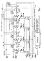
- the error correction apparatus indicated by reference numeral 10 is comprised of two major elements: a controller 12 and an ECC array 14.
- the controller 12 is connected to a microprocessor (not shown) through a bus 16 for the bi-directional transfer of data. It is also connected through a read/write line 18 for controlling the direction of data on the bus 16 and a clear line 20.
- the controller 12 is connected to the ECC array 14 through an ECC input data path 22, an ECC output data path 24, a Chien search output data path 26, and a miscellaneous control signals 28.
- the bus 16, the ECC input data path 22, the ECC output data path 24 and the Chien search output data path 26 are all eight line connections for transmitting eight bits in parallel.
- the ECC array 14 is comprised of twenty registers 30 whose inputs are respectively connected to twenty exclusive-OR gates 32.
- the two sets of inputs to the exclusive-OR gates are respectively connected one set to the outputs of twenty top multiplexers 34 and another set to the outputs of twenty bottom multiplexers 36.
- the outputs of each of the registers 30 are inversely respectively connected to twenty Galois Field multipliers So to S 19 .
- the outputs of the respective multipliers S 0 to S 19 are provided as the A inputs to the inversely corresponding top multiplexers 34.
- a highest order register 38 of the registers 30 has its outputs connected to a lead exclusive-OR gate 40, whose outputs are connected as a feedback connection through a feedback multiplexer 42 ("B" inputs) to a Galois Field parallel multiplier array 44 of the multipliers G 0 to G 19 . Additionally, the outputs of the registers 38 are provided directly as the A inputs of the feedback multiplexer 42. The outputs of the respective multipliers G 0 to G 19 of the parallel multiplier array -44 are provided as the A inputs to the correspondingly ordered bottom multiplexers 36, the outputs of which are, in turn, connected as one set of inputs to the correspondingly ordered exclusive-OR gates 32.
- the ECC input data path 22 is connected first to the exclusive-OR gate 40; second, in parallel to each of the B inputs of the bottom multiplexers 36; third, to the ECC output data path 24 via the A inputs of an output multiplexer 50; and fourth, as one set of inputs to an AND gate 46, the outputs of which are connected to the B inputs of a lowest order top multiplexer 48.
- the outputs of the registers 30, save for the register 38, are additionally respectively connected to the B inputs of the top multiplexers 34, save for the multiplexer 48.
- the outputs of the registers 30 connected to multipliers S to S 10 are additionally respectively connected as one set of inputs to nine exclusive-OR gates 52 in the following manner: the outputs from the multiplier S 10 and the outputs from the multiplier S 9 are connected as inputs to a first exclusive-OR gate 70 (see Fig. 2).
- the outputs of this exclusive-OR gate are connected as a first input set to a next exclusive-OR gate 72; the other inputs to this next exclusive-OR gate 72 are from the multiplier S 8 ; the outputs of this next exclusive-OR gate 72 are provided as a first input set to a subsequent exclusive-OR gate 74; the other input set to this subsequent exclusive-OR gate 74 being the outputs from the register S 7 , and so on until an exclusive-OR gate 64.
- the outputs of this last exclusive-OR gate 64 are provided on the C hien search output data path 26 to the controller 12.
- the number to the left of the equal sign represents the number of the output, while the numbers to the right of the equal sign represents the numbers of the inputs.
- the plus sign represents addition modulo 2, which is equivalent to an exclusive-OR gate.
- Table 2 The mathematical meaning of Table 2 can best be illustrated by example. Multiplication of two elements of GF(2 m ), y ( ⁇ ) and A ( ⁇ ), where and can be expressed which leads to
- Each of the ⁇ i is an 8-t u ple, as is the product Y ( ⁇ ) ⁇ 190 , which can be represented by Z( ⁇ ),
- Each of the inputs to the multipliers S 0 to S 19 are provided by the associated registers 30.
- each of the inputs to multipliers G 0 to G 19 are provided from a single source, the multiplexer 42. This results in the same symbol being multiplied by twenty constants, G 0 to G 19 , in parallel.
- the actual implementation of the above multiplier logic attempts to simplify the circuitry and reduce redundancy by sharing repeated logic patterns. For example, in the multiplier S 2 , the pattern "6 + 7" is repeated in equations "3" and "4". Only one "6 + 7" circuit need be implemented and its output provided as inputs to both the "3" and the "4" circuits.
- the logic associated with multipliers G 0 to G 19 may be greatly simplified by making terms appearing in many different multipliers common to all. The actual choice of circuitry implementing the logic equations is deemed to be within the skill of the art.
- an initialise line 56 is connected between the controller 12 and the clear input of each of the registers 30. Activation of the initialised line clears each of the registers 30.
- a master clock line 58 is similarly connected between the controller 12 and each of the registers 30.
- Ten ⁇ enable clock signals 60 are connected respectively to ten of the registers 30, beginning with a register 62 connected to the multiplier S1 as shown in Figure 1.
- a multiplexer select line 1 is connected to a select input of the top multiplexer 34.
- a multiplexer select line 2 is connected to a select input of the bottom multiplexer 36.
- An enable detection line is connected to the AND gate 46 and the select input of the feedback multiplexer 42.
- a read parity syndrome select line is connected to the enable input of the feedback multiplexer 42 and the select input of the output multiplexer 50. When "off" the B input of the output multiplexer 50 is selected and the feedback multiplexer 42 is disabled. When disabled, the feedback multiplexer 42 outputs all zeros.
- the transmitted code-word can be broken down into two parts: the first part, the k information symbols and the second part, the 2t parity check symbols, each symbol being eight bits in length.
- n is assumed to be equal to the length of the code word to be transmitted, and n-k equal to the number of parity check symbols.
- the transmitted code word expressed in polynomial form: where and r (X) being the remainder resulting from the division of X n-k I (X) by G(X), the generator polynomial, i.e. or Q(X) being an unused quotient, and r(X) comprising the n-k parity check symbols.
- the error correcting apparatus divides X n-k I (X) by G ( X ) and transmits the remainder r(X) so it can be appended to x n-k I(X).
- the error correcting apparatus 10 encodes the information symbols as follows: the output multiplexer 50 is initially set to output, on the ECC output data path 24, the ECC input data.
- the top multiplexers 34 are set to pass through the B inputs.
- the bottom multiplexers 36 are set to pass through the A inputs.
- the feedback multiplexer 42 is set to pass through the B inputs.
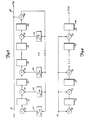
- the AND gate 46 is disabled. When so conditioned, the ECC array 14 operates as the equivalent circuit shown in Figure 3.
- the information symbols are transmitted, one by one, highest order first, along the ECC input data path 22.
- Each information symbol proceeds through the ECC input data path 22 to the lead exclusive-OR gate 40., and then through the feedback multiplexer 42 into the multiplier array 44, where the symbol is multiplied by the twenty multipliers GO to G 19 which are the coefficients of the generator polynomial G(X).
- the multiplied outputs are immediately available on the line 54 and pass through the bottom multiplexers 36 to one set of inputs to the exlusive-OR gates 32.
- the master clock is clocked once thereby causing the registers 30 to copy the information present at the exclusive-OR gates 32.
- the copied information is then available on the outputs of the registers 30.
- the outputs are multiplexed through the top multiplexers 34 (B inputs) to a second set of inputs to the exclusive-OR gates 32.
- the results of the first symbol multiplied by the multipliers GO to G 19 are exclusive-ORed with the results of the second symbol multiplied at the exclusive-OR gates 32.
- the register 30 copy the results of this exclusive-OR gate. This process continues until all information symbols have been clocked through the multiplier array 44.
- the above sequence of operations divides the information symbols, multiplied by X n-k by the generator polynomial G(X). After the division the remainder, which comprises twenty symbols, is left as a residue in the registers 30.
- the controller selects B inputs of the multiplexer 50 to connect the output of the register 38 with the ECC output data path 26; this also disables the feedback multiplexer 42. This sends all the zeros to the exclusive-OR gates 32.
- the setting of the top multiplexers 34 remains unchanged. This effectively transforms the exclusive-OR gate 32 into an OR gate to effectively transfer symbols from one register 30 to another unmodified.
- the ECC array 44 When so connected, the ECC array 44 functions as the equivalent circuit shown in Figure 4.
- the first parity symbol from the register 38 is available.
- the master clock clocks the registers, the symbols from preceding registers are copied into the next registers, and the second parity symbol is now available on the output of the register 38.
- the master clock is pulsed 19 more times or a total of 20 times to clock out each parity symbol to the ECC output data path. After all parity symbols have been clocked out, the code word C(X) is complete.
- the information symbols I(X) are provided highest order first. Assuming there are k information symbols, 2 k-1 I 0 + I i X + I ⁇ x 2 + ... I k-1 X k-1 , symbol I k-1 X k-1 appears first at the ECC input data path. This symbol is fed to the ECC array 14 for division. It also becomes the highest order C(X) output, which is an order n-k greater than in the I (X) polynomial. This transposition effectively multiplies information symbol I k-i X k-1 by X n-k , so that or
- the remainder r(X) is also provided to the ECC output data path 26 highest order first.
- the division of the code word C(X) by the generator polynomial G(X) results in a remainder r(X) having a value of zero if the code word is received without error.
- the error correcting apparatus is conditioned to divide the code word C(X) by the generator polynomial G(X) and test the remainder r(X) for a zero result by shifting the contents of the registers 30 out to the microprocessor which can perform the text for zero.
- the error correcting apparatus is conditioned in a slightly altered fashion to perform the division and testing.
- the controller 12 enables the AND gate 46 by activation of the enable detection line from the controller 12.
- the controller selects the A inputs of the bottom multiplexers 36, the B inputs of the top multiplexers 34, and the A input of the feedback multiplexer 42.
- the ECC array 44 appears as in Figure 5.
- the code word is provided, symbol-by-symbol, highest order first at the E C C data input path 22.
- the symbols are clocked through the registers 30, lowest order register to highest order register, and then fed back through the feedback multiplexer 42 into the multiplier array 44, where the highest order symbol is multiplied by the multipliers GO to G19, the coefficients of the generator polynomial.
- the process continues until each code word symbol has been clocked into a lowest order register 39, at which time the remainder from the division will be present in the registers 30.
- the B inputs of the multiplexer 50 are selected to connect the register 38 to the ECC output data path 26.
- the feedback multiplexer is disabled and 0's are provided for symbols to the exclusive-OR gates 32.
- the circuit is now equivalent to the circuit of Figure 3.
- the registers 30 are clocked 20 times providing the remainder to the microprocessor for testing for a zero value. If any of the remainder symbols are non-zero, then an error has occurred in the wode word C(X).
- the syndrome components S. can be computed by dividing R(X) by X - ⁇ 1 .
- the division results in the equality: where the remainder B. i is a constant in GF(2 m ).
- Substituting ⁇ i for X in both sides of this equation gives:
- the division can be performed as shown in Figure 6 where the received word R( X ) is provided, symbol-by-symbol, as one set of inputs to one of the exclusive-OR gate 32, which exclusive-OR is bit-by-bit the correspondingly ordered bits of its two input sets.
- the output of the exclusive-OR gate is stored, bit-by-bit, into one of the registers 30.
- the output of the register 30 is provided, bit-by-bit, to a multiply-by- ⁇ i circuit 62.
- the eight ordered outputs from the multiplier circuit 62 are provided as the second input set to the exclusive-OR gate 32.
- the selection of the A inputs of the top multiplexer 34 latches the multipliers S 0 , S 1 ... S 19 into the exclusive-OR gates 32 as shown in Figure 6.
- the selection of the B inputs of the bottom multiplexers causes the ECC input data path 22 to be coupled to the other inputs to the exclusive-OR gates 32.
- the received word R(X) is provided, symbol-by-symbol, on the ECC input data path 22, highest order first. Thereafter the ECC array is clocked n times computing the twenty syndromes S 0 , S 1 ... s 19 in parallel.
- the syndromes are present in the registers 30.
- the controller 12 selects the B input of the top multiplexers the 34 A inputs of the lower multiplexers 36 and disables the feedback multiplexer 42 to supply zero symbol data to the exclusive-OR gates 32 and clocks the ECC array 14 twenty times thereby reading out of the array along ECC output data path 24 all twenty syndromes.
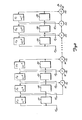
- a circuit as shown in Figure 2 performs the Chien search function.
- the circuit is comprised of ten registers 30, ten multipliers S 1 , S 2 , S 3 ... S 10 , which multiply the contents of the registers 30 by the corresponding power of a and provide feedback into the registers 30, and nine modulo 2 addition gates 52 serially connected to one another and also connected to the outputs of the registers 30.
- An additional input to register 30 comprises the coefficients of the error locator polynomial ⁇ 1 , a 2 ... ⁇ 10 . These are initally loaded into the registers 30. Thereafter the registers are clocked once 1 to form in the registers 30 the values ⁇ 10 ⁇ 10 , ⁇ 9 ⁇ 9 , ⁇ 8 ⁇ 8 ...
- the modulo 2 addition of these registers by the exclusive-OR gates 52 forms at a Chien search output at the exclusive-OR gate 64 the evaluation of the error locator polynomial at ⁇ , i.e., ⁇ ( ⁇ ) - 1.
- the outputs are evaluated by the controller 12. If the results of this evaluation are identical to 1, i.e., the eight-bit symbol at the Chien search output has only its least significant bit with non-zero value, then an error location has been found.
- the location of the error is ⁇ -1 .
- the controller When the controller identifies a Chien search output symbol having a value of 1, it signals this fact to the microprocessor. The actual location of the error is established by a counter in the microprocessor.
- the registers To evaluate the error polynomial at each possible location of the received word R(X) the registers must be clocked a total of 255 times which corresponds to the maximum length of the code word. However, one is not normally interested in errors occurring in the parity check symbols. Therefore, the registers 30 need only be clocked 255 - 2t times, where t is the number of errors, as the parity check symbols occur in the lowest order locations of the code word R(X), i.e.,
- the controller 12 conditions the ECC array 14 to perform the Chien search function by initially loading the coefficients of the error locator polynomials ⁇ (X) into the registers 30 corresponding to multipliers S 1 to S 10 as follows: the registers 30 are first initialised to zero and the B inputs of the bottom multiplexers are selected thereby connecting the ECC input data path 22 to the exclusive-OR gates 32. As the contents of the registers 30 are zero, the exclusive-OR gates 32 will pass the information on the ECC input data path 22 unchanged into the registers 30 if the information is loaded into the registers from right to left in the figure. Thus the coefficients of the error polynomial ⁇ (X) are presented with the lowest order coefficient a first and the highest order coefficient ⁇ 10 last.
- the controller 12 When ⁇ 1 is transmitted to the ECC array 14 by the microprocessor, the controller 12 enables and clocks the register 62 via the ⁇ 1 enable clock signals 60. A similar procedure is performed for a 2 to a 10 individually clocking into the registers 30 the respective coefficients of the error locator polynomial. Once the coefficients have been loaded, the controller 12 presents symbols of zero value on the ECC input data path 22 thereby effectively changing the exclusive-OR gates 32 into OR gates which pass the information presented by the upper multiplexers unchanged into the registers 30. The controller selects the A inputs of the upper multiplexers 34 to connect the multipliers S 1 to S 10 into exclusive-OR gates 32. The registers 30 are then clocked once to evaluate the error locator polynomial at ⁇ 1 .
- the outputs of the multipliers S to S 10 are fed into the exclusive-OR gates 52 connected as shown in Figure 2 so that the modulo 2 sum of the registers appears at the Chien search output.
- This output is provided as a feedback to the controller 12 which in turn, provides it as feedback to the microprocessor.
- the controller clocks the registers 2 m - 2t -1 times where m is the length of the code symbol and 2t are the number of parity check symbols.
- the values of the error at the locations can be found by solving the error value formula for the Y. as described above.
- the error correcting apparatus of the present invention can also perform burst error trapping.
- Reed-Solomon codes are cyclic and therefore may be used for trapping single burst errors to a maximum length of t, where t is the error correction capability of the code, provided the errors are confined to contiguous symbols within a code word.
- the controller 12 selects the B inputs of the upper multiplexers 34, the A input of the bottom multiplexers 36 and the B input of the multiplexer 42.
- the arrangement is set to divide the received word X n-k R(X) by the generator polynomial G(X).
- the incoming received word R(X) is cycled symbol-by-symbol highest order first.
- the ECC array 14 is clocked n times for the n symbols of the received word R(X). After all the symbols of the received word R ( X ) have been clocked into the ECC array 14, the controller 12 disables the ECC input data path 22 by providing all-zero symbols.
- the controller clocks the registers 30 an additional n-2t times where n is the length of the code or until t or more zeros are detected at the encoder output data path.
- the magnitude of the burst error now exists in the next t or fewer registers 30 and may be used for the correction of the burst error by direct modulo 2 addition of the contents of the next t or fewer non-zero symbols to the correspondingly shifted received word symbols. See, e.g., Chapter 11 of Peterson and Weldon, Error-Correcting Codes, 2nd Ed. (1972), especially at Section 11.3.
Landscapes
- Physics & Mathematics (AREA)
- Mathematical Physics (AREA)
- Algebra (AREA)
- General Physics & Mathematics (AREA)
- Pure & Applied Mathematics (AREA)
- Probability & Statistics with Applications (AREA)
- Engineering & Computer Science (AREA)
- Theoretical Computer Science (AREA)
- Error Detection And Correction (AREA)
Applications Claiming Priority (2)
| Application Number | Priority Date | Filing Date | Title |
|---|---|---|---|
| US06/564,273 US4584686A (en) | 1983-12-22 | 1983-12-22 | Reed-Solomon error correction apparatus |
| US564273 | 1983-12-22 |
Publications (3)
| Publication Number | Publication Date |
|---|---|
| EP0147041A2 true EP0147041A2 (fr) | 1985-07-03 |
| EP0147041A3 EP0147041A3 (en) | 1988-02-03 |
| EP0147041B1 EP0147041B1 (fr) | 1991-04-24 |
Family
ID=24253818
Family Applications (1)
| Application Number | Title | Priority Date | Filing Date |
|---|---|---|---|
| EP84307709A Expired EP0147041B1 (fr) | 1983-12-22 | 1984-11-08 | Dispositif de protection d'erreurs |
Country Status (5)
| Country | Link |
|---|---|
| US (1) | US4584686A (fr) |
| EP (1) | EP0147041B1 (fr) |
| JP (1) | JPS60223230A (fr) |
| CA (1) | CA1222829A (fr) |
| DE (1) | DE3484503D1 (fr) |
Cited By (10)
| Publication number | Priority date | Publication date | Assignee | Title |
|---|---|---|---|---|
| EP0249982A2 (fr) * | 1986-06-18 | 1987-12-23 | Mitsubishi Denki Kabushiki Kaisha | Décodeur |
| EP0271082A2 (fr) * | 1986-12-10 | 1988-06-15 | Matsushita Electric Industrial Co., Ltd. | Unité arithmétique et logique utilisant des éléments des champs de Galois |
| EP0329775A1 (fr) * | 1987-08-24 | 1989-08-30 | Quantum Corporation | Circuit de codage, decodage et de correction d'erreur reed-solomon a grande largeur de bande |
| EP0442320A1 (fr) * | 1990-02-14 | 1991-08-21 | ALCATEL ITALIA Società per Azioni | Procédé et système pour la correction d'erreurs dans la transmission numérique |
| FR2717968A1 (fr) * | 1994-03-25 | 1995-09-29 | Mitsubishi Electric Corp | Codeur exécutant une correction d'erreurs, décodeur exécutant une correction d'erreurs et système de transmission de données utilisant des codes de correction d'erreurs. |
| FR2721774A1 (fr) * | 1994-06-27 | 1995-12-29 | Sgs Thomson Microelectronics | Décodeur reed-solomon. |
| EP0723342A2 (fr) * | 1986-09-30 | 1996-07-24 | Canon Kabushiki Kaisha | Appareil de correction d'erreurs |
| WO1997011530A1 (fr) * | 1995-09-20 | 1997-03-27 | Hitachi, Ltd. | Procede de decodage d'une grappe d'erreurs du code de reed-solomon et dispositif correspondant |
| US5912905A (en) * | 1994-03-25 | 1999-06-15 | Mitsubishi Denki Kabushiki Kaisha | Error-correcting encoder, error-correcting decoder and data transmitting system with error-correcting codes |
| DE19747774B4 (de) * | 1996-10-29 | 2009-07-09 | Daewoo Electronics Corp. | Reed-Solomon-Decoder zur Verwendung beim verbesserten Fernsehen (ATV) |
Families Citing this family (108)
| Publication number | Priority date | Publication date | Assignee | Title |
|---|---|---|---|---|
| JPS60186942A (ja) * | 1984-02-24 | 1985-09-24 | Victor Co Of Japan Ltd | デイジタル乗算回路 |
| US5027315A (en) * | 1984-09-28 | 1991-06-25 | Advanced Micro Devices, Inc. | Programmable logic array using internally generated dynamic logic signals as selection signals for controlling its functions |
| US4747103A (en) * | 1985-03-21 | 1988-05-24 | Canon Kabushiki Kaisha | Signal processing apparatus for correcting decoding errors |
| JPH0728227B2 (ja) * | 1985-06-07 | 1995-03-29 | ソニー株式会社 | Bch符号の復号装置 |
| US4845713A (en) * | 1987-06-08 | 1989-07-04 | Exabyte Corporation | Method and apparatus for determining the coefficients of a locator polynomial |
| EP0329789B1 (fr) * | 1987-06-30 | 1995-02-08 | Matsushita Electric Industrial Co., Ltd. | Unite arithmetique a champ de galois |
| US4979173A (en) * | 1987-09-21 | 1990-12-18 | Cirrus Logic, Inc. | Burst mode error detection and definition |
| US5140595A (en) * | 1987-09-21 | 1992-08-18 | Cirrus Logic, Inc. | Burst mode error detection and definition |
| US4835775A (en) * | 1987-10-13 | 1989-05-30 | Cyclotomics, Inc. | Hypersystolic reed-solomon encoder |
| US4843607A (en) * | 1987-12-17 | 1989-06-27 | Cyclotomics, Inc. | Multiple error trapping |
| US4916702A (en) * | 1988-06-17 | 1990-04-10 | Cyclotomics, Inc. | Elongated burst trapping |
| JPH0267013A (ja) * | 1988-09-01 | 1990-03-07 | Mitsubishi Electric Corp | ガロア体演算回路 |
| US5107506A (en) * | 1990-01-25 | 1992-04-21 | Digital Equipment Corporation | Error trapping decoding method and apparatus |
| US5280488A (en) * | 1990-11-08 | 1994-01-18 | Neal Glover | Reed-Solomon code system employing k-bit serial techniques for encoding and burst error trapping |
| JPH04315332A (ja) * | 1991-04-15 | 1992-11-06 | Hitachi Ltd | 誤り訂正装置 |
| US5638386A (en) * | 1991-09-20 | 1997-06-10 | Hitachi, Ltd. | Recording apparatus |
| US5329535A (en) * | 1992-04-30 | 1994-07-12 | International Business Machines Corporation | Variable block lengths on-the-fly error correcting decoder |
| US5444719A (en) * | 1993-01-26 | 1995-08-22 | International Business Machines Corporation | Adjustable error-correction composite Reed-Solomon encoder/syndrome generator |
| JPH06314978A (ja) * | 1993-04-28 | 1994-11-08 | Nec Corp | チェン・サーチ回路 |
| US5463642A (en) * | 1993-06-29 | 1995-10-31 | Mitsubishi Semiconductor America, Inc. | Method and apparatus for determining error location |
| US5465261A (en) * | 1993-08-03 | 1995-11-07 | National Semiconductor Corporation | RAM based architecture for ECC circuits |
| US5642367A (en) * | 1994-02-07 | 1997-06-24 | Mitsubishi Semiconductor America, Inc. | Finite field polynomial processing module for error control coding |
| US5771244A (en) * | 1994-03-09 | 1998-06-23 | University Of Southern California | Universal Reed-Solomon coder/encoder |
| US5936978A (en) * | 1996-12-05 | 1999-08-10 | Telefonaktiebolaget L M Ericsson (Publ) | Shortened fire code error-trapping decoding method and apparatus |
| KR100480685B1 (ko) * | 1997-04-04 | 2005-05-16 | 엘지전자 주식회사 | 에러정정회로 |
| US5970075A (en) * | 1997-06-18 | 1999-10-19 | Uniden San Diego Research And Development Center Inc. | Method and apparatus for generating an error location polynomial table |
| US6163871A (en) * | 1998-05-29 | 2000-12-19 | Adaptec, Inc. | RAM based error correction code encoder and syndrome generator with programmable interleaving degrees |
| US6279137B1 (en) | 1998-12-08 | 2001-08-21 | Lsi Logic Corporation | System and method for a storage-efficient parallel Chien Search |
| US6571368B1 (en) * | 2000-02-02 | 2003-05-27 | Macronix International Co., Ltd. | Systolic Reed-Solomon decoder |
| US7155656B1 (en) * | 2003-05-01 | 2006-12-26 | Hellosoft Inc. | Method and system for decoding of binary shortened cyclic code |
| TWI309364B (en) * | 2005-09-02 | 2009-05-01 | Infortrend Technology Inc | Method and controller for processing data multiplication in raid system |
| US20070089023A1 (en) * | 2005-09-30 | 2007-04-19 | Sigmatel, Inc. | System and method for system resource access |
| US20070268905A1 (en) * | 2006-05-18 | 2007-11-22 | Sigmatel, Inc. | Non-volatile memory error correction system and method |
| WO2009095902A2 (fr) | 2008-01-31 | 2009-08-06 | Densbits Technologies Ltd. | Systèmes et procédés pour traiter des erreurs de données immédiates dans une mémoire flash |
| US8650352B2 (en) * | 2007-09-20 | 2014-02-11 | Densbits Technologies Ltd. | Systems and methods for determining logical values of coupled flash memory cells |
| US8694715B2 (en) | 2007-10-22 | 2014-04-08 | Densbits Technologies Ltd. | Methods for adaptively programming flash memory devices and flash memory systems incorporating same |
| WO2009053961A2 (fr) | 2007-10-25 | 2009-04-30 | Densbits Technologies Ltd. | Systèmes et procédés pour rendements de codage multiples dans des dispositifs flash |
| US8335977B2 (en) | 2007-12-05 | 2012-12-18 | Densbits Technologies Ltd. | Flash memory apparatus and methods using a plurality of decoding stages including optional use of concatenated BCH codes and/or designation of “first below” cells |
| US8453022B2 (en) | 2007-12-05 | 2013-05-28 | Densbits Technologies Ltd. | Apparatus and methods for generating row-specific reading thresholds in flash memory |
| US8607128B2 (en) | 2007-12-05 | 2013-12-10 | Densbits Technologies Ltd. | Low power chien-search based BCH/RS decoding system for flash memory, mobile communications devices and other applications |
| WO2009074979A2 (fr) * | 2007-12-12 | 2009-06-18 | Densbits Technologies Ltd. | Système de recherche de chien employant un schéma de désactivation du signal d'horloge pour économiser de l'énergie pour un décodeur correcteur d'erreurs et autres applications |
| US8359516B2 (en) | 2007-12-12 | 2013-01-22 | Densbits Technologies Ltd. | Systems and methods for error correction and decoding on multi-level physical media |
| WO2009078006A2 (fr) | 2007-12-18 | 2009-06-25 | Densbits Technologies Ltd. | Appareil pour le codage avec une pluralité de vitesses dans des systèmes de mémoires flash à niveaux multiples et procédés utiles associés |
| WO2009118720A2 (fr) * | 2008-03-25 | 2009-10-01 | Densbits Technologies Ltd. | Appareil et procédés pour l’arrondi non biaisé à efficacité matérielle |
| US8332725B2 (en) | 2008-08-20 | 2012-12-11 | Densbits Technologies Ltd. | Reprogramming non volatile memory portions |
| US8407554B2 (en) * | 2009-02-03 | 2013-03-26 | Complete Genomics, Inc. | Method and apparatus for quantification of DNA sequencing quality and construction of a characterizable model system using Reed-Solomon codes |
| US8762818B1 (en) * | 2009-03-05 | 2014-06-24 | Marvell International Ltd. | System and methods for performing decoding error detection in a storage device |
| US8819385B2 (en) | 2009-04-06 | 2014-08-26 | Densbits Technologies Ltd. | Device and method for managing a flash memory |
| US8458574B2 (en) * | 2009-04-06 | 2013-06-04 | Densbits Technologies Ltd. | Compact chien-search based decoding apparatus and method |
| US8566510B2 (en) | 2009-05-12 | 2013-10-22 | Densbits Technologies Ltd. | Systems and method for flash memory management |
| US8995197B1 (en) | 2009-08-26 | 2015-03-31 | Densbits Technologies Ltd. | System and methods for dynamic erase and program control for flash memory device memories |
| US8868821B2 (en) | 2009-08-26 | 2014-10-21 | Densbits Technologies Ltd. | Systems and methods for pre-equalization and code design for a flash memory |
| US8305812B2 (en) * | 2009-08-26 | 2012-11-06 | Densbits Technologies Ltd. | Flash memory module and method for programming a page of flash memory cells |
| US9330767B1 (en) | 2009-08-26 | 2016-05-03 | Avago Technologies General Ip (Singapore) Pte. Ltd. | Flash memory module and method for programming a page of flash memory cells |
| US8730729B2 (en) | 2009-10-15 | 2014-05-20 | Densbits Technologies Ltd. | Systems and methods for averaging error rates in non-volatile devices and storage systems |
| US8724387B2 (en) | 2009-10-22 | 2014-05-13 | Densbits Technologies Ltd. | Method, system, and computer readable medium for reading and programming flash memory cells using multiple bias voltages |
| US8626988B2 (en) * | 2009-11-19 | 2014-01-07 | Densbits Technologies Ltd. | System and method for uncoded bit error rate equalization via interleaving |
| US9037777B2 (en) * | 2009-12-22 | 2015-05-19 | Densbits Technologies Ltd. | Device, system, and method for reducing program/read disturb in flash arrays |
| US8607124B2 (en) * | 2009-12-24 | 2013-12-10 | Densbits Technologies Ltd. | System and method for setting a flash memory cell read threshold |
| US8700970B2 (en) * | 2010-02-28 | 2014-04-15 | Densbits Technologies Ltd. | System and method for multi-dimensional decoding |
| US8527840B2 (en) | 2010-04-06 | 2013-09-03 | Densbits Technologies Ltd. | System and method for restoring damaged data programmed on a flash device |
| US9104610B2 (en) | 2010-04-06 | 2015-08-11 | Densbits Technologies Ltd. | Method, system and medium for analog encryption in a flash memory |
| US8745317B2 (en) | 2010-04-07 | 2014-06-03 | Densbits Technologies Ltd. | System and method for storing information in a multi-level cell memory |
| US9021177B2 (en) | 2010-04-29 | 2015-04-28 | Densbits Technologies Ltd. | System and method for allocating and using spare blocks in a flash memory |
| US8468431B2 (en) | 2010-07-01 | 2013-06-18 | Densbits Technologies Ltd. | System and method for multi-dimensional encoding and decoding |
| US8539311B2 (en) | 2010-07-01 | 2013-09-17 | Densbits Technologies Ltd. | System and method for data recovery in multi-level cell memories |
| US8467249B2 (en) | 2010-07-06 | 2013-06-18 | Densbits Technologies Ltd. | Systems and methods for storing, retrieving, and adjusting read thresholds in flash memory storage system |
| US8964464B2 (en) | 2010-08-24 | 2015-02-24 | Densbits Technologies Ltd. | System and method for accelerated sampling |
| US8508995B2 (en) | 2010-09-15 | 2013-08-13 | Densbits Technologies Ltd. | System and method for adjusting read voltage thresholds in memories |
| US9063878B2 (en) | 2010-11-03 | 2015-06-23 | Densbits Technologies Ltd. | Method, system and computer readable medium for copy back |
| US8850100B2 (en) | 2010-12-07 | 2014-09-30 | Densbits Technologies Ltd. | Interleaving codeword portions between multiple planes and/or dies of a flash memory device |
| US10079068B2 (en) | 2011-02-23 | 2018-09-18 | Avago Technologies General Ip (Singapore) Pte. Ltd. | Devices and method for wear estimation based memory management |
| US8693258B2 (en) | 2011-03-17 | 2014-04-08 | Densbits Technologies Ltd. | Obtaining soft information using a hard interface |
| US8990665B1 (en) | 2011-04-06 | 2015-03-24 | Densbits Technologies Ltd. | System, method and computer program product for joint search of a read threshold and soft decoding |
| US9195592B1 (en) | 2011-05-12 | 2015-11-24 | Densbits Technologies Ltd. | Advanced management of a non-volatile memory |
| US8996790B1 (en) | 2011-05-12 | 2015-03-31 | Densbits Technologies Ltd. | System and method for flash memory management |
| US9396106B2 (en) | 2011-05-12 | 2016-07-19 | Avago Technologies General Ip (Singapore) Pte. Ltd. | Advanced management of a non-volatile memory |
| US9110785B1 (en) | 2011-05-12 | 2015-08-18 | Densbits Technologies Ltd. | Ordered merge of data sectors that belong to memory space portions |
| US9501392B1 (en) | 2011-05-12 | 2016-11-22 | Avago Technologies General Ip (Singapore) Pte. Ltd. | Management of a non-volatile memory module |
| US9372792B1 (en) | 2011-05-12 | 2016-06-21 | Avago Technologies General Ip (Singapore) Pte. Ltd. | Advanced management of a non-volatile memory |
| US8667211B2 (en) | 2011-06-01 | 2014-03-04 | Densbits Technologies Ltd. | System and method for managing a non-volatile memory |
| US8588003B1 (en) | 2011-08-01 | 2013-11-19 | Densbits Technologies Ltd. | System, method and computer program product for programming and for recovering from a power failure |
| US8553468B2 (en) | 2011-09-21 | 2013-10-08 | Densbits Technologies Ltd. | System and method for managing erase operations in a non-volatile memory |
| US8996788B2 (en) | 2012-02-09 | 2015-03-31 | Densbits Technologies Ltd. | Configurable flash interface |
| US8947941B2 (en) | 2012-02-09 | 2015-02-03 | Densbits Technologies Ltd. | State responsive operations relating to flash memory cells |
| US8996793B1 (en) | 2012-04-24 | 2015-03-31 | Densbits Technologies Ltd. | System, method and computer readable medium for generating soft information |
| US8838937B1 (en) | 2012-05-23 | 2014-09-16 | Densbits Technologies Ltd. | Methods, systems and computer readable medium for writing and reading data |
| US8879325B1 (en) | 2012-05-30 | 2014-11-04 | Densbits Technologies Ltd. | System, method and computer program product for processing read threshold information and for reading a flash memory module |
| US9921954B1 (en) | 2012-08-27 | 2018-03-20 | Avago Technologies General Ip (Singapore) Pte. Ltd. | Method and system for split flash memory management between host and storage controller |
| US9368225B1 (en) | 2012-11-21 | 2016-06-14 | Avago Technologies General Ip (Singapore) Pte. Ltd. | Determining read thresholds based upon read error direction statistics |
| US9069659B1 (en) | 2013-01-03 | 2015-06-30 | Densbits Technologies Ltd. | Read threshold determination using reference read threshold |
| US9136876B1 (en) | 2013-06-13 | 2015-09-15 | Densbits Technologies Ltd. | Size limited multi-dimensional decoding |
| US9413491B1 (en) | 2013-10-08 | 2016-08-09 | Avago Technologies General Ip (Singapore) Pte. Ltd. | System and method for multiple dimension decoding and encoding a message |
| US9397706B1 (en) | 2013-10-09 | 2016-07-19 | Avago Technologies General Ip (Singapore) Pte. Ltd. | System and method for irregular multiple dimension decoding and encoding |
| US9348694B1 (en) | 2013-10-09 | 2016-05-24 | Avago Technologies General Ip (Singapore) Pte. Ltd. | Detecting and managing bad columns |
| US9786388B1 (en) | 2013-10-09 | 2017-10-10 | Avago Technologies General Ip (Singapore) Pte. Ltd. | Detecting and managing bad columns |
| US9536612B1 (en) | 2014-01-23 | 2017-01-03 | Avago Technologies General Ip (Singapore) Pte. Ltd | Digital signaling processing for three dimensional flash memory arrays |
| US10120792B1 (en) | 2014-01-29 | 2018-11-06 | Avago Technologies General Ip (Singapore) Pte. Ltd. | Programming an embedded flash storage device |
| US9542262B1 (en) | 2014-05-29 | 2017-01-10 | Avago Technologies General Ip (Singapore) Pte. Ltd. | Error correction |
| US9892033B1 (en) | 2014-06-24 | 2018-02-13 | Avago Technologies General Ip (Singapore) Pte. Ltd. | Management of memory units |
| US9972393B1 (en) | 2014-07-03 | 2018-05-15 | Avago Technologies General Ip (Singapore) Pte. Ltd. | Accelerating programming of a flash memory module |
| US9584159B1 (en) | 2014-07-03 | 2017-02-28 | Avago Technologies General Ip (Singapore) Pte. Ltd. | Interleaved encoding |
| US9449702B1 (en) | 2014-07-08 | 2016-09-20 | Avago Technologies General Ip (Singapore) Pte. Ltd. | Power management |
| US9524211B1 (en) | 2014-11-18 | 2016-12-20 | Avago Technologies General Ip (Singapore) Pte. Ltd. | Codeword management |
| US10305515B1 (en) | 2015-02-02 | 2019-05-28 | Avago Technologies International Sales Pte. Limited | System and method for encoding using multiple linear feedback shift registers |
| US10628255B1 (en) | 2015-06-11 | 2020-04-21 | Avago Technologies International Sales Pte. Limited | Multi-dimensional decoding |
| US9851921B1 (en) | 2015-07-05 | 2017-12-26 | Avago Technologies General Ip (Singapore) Pte. Ltd. | Flash memory chip processing |
| US9954558B1 (en) | 2016-03-03 | 2018-04-24 | Avago Technologies General Ip (Singapore) Pte. Ltd. | Fast decoding of data stored in a flash memory |
Citations (2)
| Publication number | Priority date | Publication date | Assignee | Title |
|---|---|---|---|---|
| US3648236A (en) * | 1970-04-20 | 1972-03-07 | Bell Telephone Labor Inc | Decoding method and apparatus for bose-chaudhuri-hocquenghem codes |
| EP0096109A2 (fr) * | 1982-06-15 | 1983-12-21 | Kabushiki Kaisha Toshiba | Système de correction d'erreurs |
Family Cites Families (3)
| Publication number | Priority date | Publication date | Assignee | Title |
|---|---|---|---|---|
| US4162480A (en) * | 1977-01-28 | 1979-07-24 | Cyclotomics, Inc. | Galois field computer |
| US4142174A (en) * | 1977-08-15 | 1979-02-27 | International Business Machines Corporation | High speed decoding of Reed-Solomon codes |
| US4410989A (en) * | 1980-12-11 | 1983-10-18 | Cyclotomics, Inc. | Bit serial encoder |
-
1983
- 1983-12-22 US US06/564,273 patent/US4584686A/en not_active Expired - Fee Related
-
1984
- 1984-11-08 EP EP84307709A patent/EP0147041B1/fr not_active Expired
- 1984-11-08 DE DE8484307709T patent/DE3484503D1/de not_active Expired - Lifetime
- 1984-11-19 CA CA000468136A patent/CA1222829A/fr not_active Expired
- 1984-11-26 JP JP59249424A patent/JPS60223230A/ja active Granted
Patent Citations (2)
| Publication number | Priority date | Publication date | Assignee | Title |
|---|---|---|---|---|
| US3648236A (en) * | 1970-04-20 | 1972-03-07 | Bell Telephone Labor Inc | Decoding method and apparatus for bose-chaudhuri-hocquenghem codes |
| EP0096109A2 (fr) * | 1982-06-15 | 1983-12-21 | Kabushiki Kaisha Toshiba | Système de correction d'erreurs |
Non-Patent Citations (2)
| Title |
|---|
| IEEE TRANSACTIONS ON COMPUTERS, vol. C-31, no. 2, February 1982, pages 170-175, IEEE, New York, US; K.Y. LIU: "Architecture for VLSI design of Reed-Solomon encoders" * |
| PROCEEDINGS OF SPIE-THE INTERNATIONAL SOCIETY FOR OPTICAL ENGINEERING, Arlington, Virginia, 8th-9th June 1983, vol. 421, pages 65-78, Bellingham, Washington, US; S. DEODHAR et al.: "High speed interleaved Reed-Solomon error detection and correction system" * |
Cited By (17)
| Publication number | Priority date | Publication date | Assignee | Title |
|---|---|---|---|---|
| EP0249982A3 (en) * | 1986-06-18 | 1990-12-27 | Mitsubishi Denki Kabushiki Kaisha | Decoder |
| EP0249982A2 (fr) * | 1986-06-18 | 1987-12-23 | Mitsubishi Denki Kabushiki Kaisha | Décodeur |
| EP0723342A3 (fr) * | 1986-09-30 | 1997-08-20 | Canon Kk | Appareil de correction d'erreurs |
| EP0723342A2 (fr) * | 1986-09-30 | 1996-07-24 | Canon Kabushiki Kaisha | Appareil de correction d'erreurs |
| US5774389A (en) * | 1986-09-30 | 1998-06-30 | Canon Kabushiki Kaisha | Error correction apparatus |
| EP0271082A2 (fr) * | 1986-12-10 | 1988-06-15 | Matsushita Electric Industrial Co., Ltd. | Unité arithmétique et logique utilisant des éléments des champs de Galois |
| EP0271082A3 (en) * | 1986-12-10 | 1990-05-23 | Matsushita Electric Industrial Co., Ltd. | Galois field arithmetic logic unit |
| EP0329775A4 (en) * | 1987-08-24 | 1991-09-25 | Digital Equipment Corporation | High bandwidth reed-solomon encoding, decoding and error correcting circuit |
| EP0329775A1 (fr) * | 1987-08-24 | 1989-08-30 | Quantum Corporation | Circuit de codage, decodage et de correction d'erreur reed-solomon a grande largeur de bande |
| EP0442320A1 (fr) * | 1990-02-14 | 1991-08-21 | ALCATEL ITALIA Società per Azioni | Procédé et système pour la correction d'erreurs dans la transmission numérique |
| FR2717968A1 (fr) * | 1994-03-25 | 1995-09-29 | Mitsubishi Electric Corp | Codeur exécutant une correction d'erreurs, décodeur exécutant une correction d'erreurs et système de transmission de données utilisant des codes de correction d'erreurs. |
| US5699368A (en) * | 1994-03-25 | 1997-12-16 | Mitsubishi Denki Kabushiki Kaisha | Error-correcting encoder, error-correcting decoder, and data transmitting system with error-correcting codes |
| US5912905A (en) * | 1994-03-25 | 1999-06-15 | Mitsubishi Denki Kabushiki Kaisha | Error-correcting encoder, error-correcting decoder and data transmitting system with error-correcting codes |
| FR2721774A1 (fr) * | 1994-06-27 | 1995-12-29 | Sgs Thomson Microelectronics | Décodeur reed-solomon. |
| EP0690585A1 (fr) * | 1994-06-27 | 1996-01-03 | STMicroelectronics S.A. | Décodeur Reed-Solomon |
| WO1997011530A1 (fr) * | 1995-09-20 | 1997-03-27 | Hitachi, Ltd. | Procede de decodage d'une grappe d'erreurs du code de reed-solomon et dispositif correspondant |
| DE19747774B4 (de) * | 1996-10-29 | 2009-07-09 | Daewoo Electronics Corp. | Reed-Solomon-Decoder zur Verwendung beim verbesserten Fernsehen (ATV) |
Also Published As
| Publication number | Publication date |
|---|---|
| JPH0464211B2 (fr) | 1992-10-14 |
| EP0147041A3 (en) | 1988-02-03 |
| CA1222829A (fr) | 1987-06-09 |
| US4584686A (en) | 1986-04-22 |
| EP0147041B1 (fr) | 1991-04-24 |
| JPS60223230A (ja) | 1985-11-07 |
| DE3484503D1 (de) | 1991-05-29 |
Similar Documents
| Publication | Publication Date | Title |
|---|---|---|
| US4584686A (en) | Reed-Solomon error correction apparatus | |
| US6374383B1 (en) | Determining error locations using error correction codes | |
| US5491701A (en) | Burst error corrector | |
| US4782490A (en) | Method and a system for multiple error detection and correction | |
| US6615387B1 (en) | Method and apparatus for error detection | |
| EP1131893B1 (fr) | Correcteur d'erreurs sans voie de retour | |
| US4504948A (en) | Syndrome processing unit for multibyte error correcting systems | |
| US5467297A (en) | Finite field inversion | |
| US8176396B2 (en) | System and method for implementing a Reed Solomon multiplication section from exclusive-OR logic | |
| EP0233075B1 (fr) | Méthode et appareil pour générer des bytes de contrôle pour la détection d'erreurs dans des blocs de données | |
| US5805617A (en) | Apparatus for computing error correction syndromes | |
| US4527269A (en) | Encoder verifier | |
| US20130139028A1 (en) | Extended Bidirectional Hamming Code for Double-Error Correction and Triple-Error Detection | |
| US10812109B2 (en) | Determination and use of byte error position signals | |
| EP0753942A2 (fr) | Traitement par mot pour des codes Reed-Solomon | |
| JPH0728227B2 (ja) | Bch符号の復号装置 | |
| KR100192795B1 (ko) | 리드 솔로몬 복호기의 에러 위치 다항식 계산 장치 | |
| US5822337A (en) | Programmable redundancy/syndrome generator | |
| US7096408B1 (en) | Method and apparatus for computing the error locator polynomial in a decoder of a forward error correction (FEC) system | |
| KR100258951B1 (ko) | 리드-솔로몬(rs) 복호기와 그 복호방법 | |
| US6643819B1 (en) | Hybrid root-finding technique | |
| US6405339B1 (en) | Parallelized programmable encoder/syndrome generator | |
| US5971607A (en) | Polynomial evaluator for use in a Reed-Solomon decoder | |
| EP0793352B1 (fr) | Appareil pour la détermination du polynÔme d'évaluation des erreurs dans un décodeur Reed-Solomon | |
| Khan et al. | Hardware implementation of shortened (48, 38) Reed Solomon forward error correcting code |
Legal Events
| Date | Code | Title | Description |
|---|---|---|---|
| PUAI | Public reference made under article 153(3) epc to a published international application that has entered the european phase |
Free format text: ORIGINAL CODE: 0009012 |
|
| AK | Designated contracting states |
Designated state(s): DE FR GB NL |
|
| RAP1 | Party data changed (applicant data changed or rights of an application transferred) |
Owner name: LASER MAGNETIC STORAGE INTERNATIONAL COMPANY |
|
| PUAL | Search report despatched |
Free format text: ORIGINAL CODE: 0009013 |
|
| RHK1 | Main classification (correction) |
Ipc: H03M 13/00 |
|
| AK | Designated contracting states |
Kind code of ref document: A3 Designated state(s): DE FR GB NL |
|
| 17P | Request for examination filed |
Effective date: 19880804 |
|
| R17P | Request for examination filed (corrected) |
Effective date: 19880802 |
|
| 17Q | First examination report despatched |
Effective date: 19890911 |
|
| GRAA | (expected) grant |
Free format text: ORIGINAL CODE: 0009210 |
|
| AK | Designated contracting states |
Kind code of ref document: B1 Designated state(s): DE FR GB NL |
|
| PG25 | Lapsed in a contracting state [announced via postgrant information from national office to epo] |
Ref country code: NL Effective date: 19910424 |
|
| REF | Corresponds to: |
Ref document number: 3484503 Country of ref document: DE Date of ref document: 19910529 |
|
| ET | Fr: translation filed | ||
| NLV1 | Nl: lapsed or annulled due to failure to fulfill the requirements of art. 29p and 29m of the patents act | ||
| PLBE | No opposition filed within time limit |
Free format text: ORIGINAL CODE: 0009261 |
|
| STAA | Information on the status of an ep patent application or granted ep patent |
Free format text: STATUS: NO OPPOSITION FILED WITHIN TIME LIMIT |
|
| 26N | No opposition filed | ||
| REG | Reference to a national code |
Ref country code: GB Ref legal event code: 732 |
|
| REG | Reference to a national code |
Ref country code: FR Ref legal event code: TP |
|
| PGFP | Annual fee paid to national office [announced via postgrant information from national office to epo] |
Ref country code: DE Payment date: 19950124 Year of fee payment: 11 |
|
| REG | Reference to a national code |
Ref country code: FR Ref legal event code: CD |
|
| PGFP | Annual fee paid to national office [announced via postgrant information from national office to epo] |
Ref country code: GB Payment date: 19951101 Year of fee payment: 12 |
|
| PGFP | Annual fee paid to national office [announced via postgrant information from national office to epo] |
Ref country code: FR Payment date: 19951129 Year of fee payment: 12 |
|
| PG25 | Lapsed in a contracting state [announced via postgrant information from national office to epo] |
Ref country code: DE Effective date: 19960801 |
|
| PG25 | Lapsed in a contracting state [announced via postgrant information from national office to epo] |
Ref country code: GB Effective date: 19961108 |
|
| GBPC | Gb: european patent ceased through non-payment of renewal fee |
Effective date: 19961108 |
|
| PG25 | Lapsed in a contracting state [announced via postgrant information from national office to epo] |
Ref country code: FR Effective date: 19970731 |
|
| REG | Reference to a national code |
Ref country code: FR Ref legal event code: ST |