EP0144835B1 - PCM-Rahmensynchronisierungseinheit - Google Patents
PCM-Rahmensynchronisierungseinheit Download PDFInfo
- Publication number
- EP0144835B1 EP0144835B1 EP84113843A EP84113843A EP0144835B1 EP 0144835 B1 EP0144835 B1 EP 0144835B1 EP 84113843 A EP84113843 A EP 84113843A EP 84113843 A EP84113843 A EP 84113843A EP 0144835 B1 EP0144835 B1 EP 0144835B1
- Authority
- EP
- European Patent Office
- Prior art keywords
- signal
- channel
- pcm
- frame
- apt
- Prior art date
- Legal status (The legal status is an assumption and is not a legal conclusion. Google has not performed a legal analysis and makes no representation as to the accuracy of the status listed.)
- Expired
Links
- 230000006870 function Effects 0.000 claims description 9
- 238000012163 sequencing technique Methods 0.000 claims description 6
- 230000000295 complement effect Effects 0.000 claims description 5
- 230000001360 synchronised effect Effects 0.000 claims description 2
- 108091006146 Channels Proteins 0.000 description 56
- 238000010586 diagram Methods 0.000 description 9
- 238000003745 diagnosis Methods 0.000 description 2
- 230000007704 transition Effects 0.000 description 2
- 230000002457 bidirectional effect Effects 0.000 description 1
- 230000005540 biological transmission Effects 0.000 description 1
- 238000013500 data storage Methods 0.000 description 1
- 230000000694 effects Effects 0.000 description 1
- 238000012423 maintenance Methods 0.000 description 1
- 230000008929 regeneration Effects 0.000 description 1
- 238000011069 regeneration method Methods 0.000 description 1
- 230000008054 signal transmission Effects 0.000 description 1
- 230000011664 signaling Effects 0.000 description 1
Images


Classifications
-
- H—ELECTRICITY
- H04—ELECTRIC COMMUNICATION TECHNIQUE
- H04N—PICTORIAL COMMUNICATION, e.g. TELEVISION
- H04N21/00—Selective content distribution, e.g. interactive television or video on demand [VOD]
- H04N21/20—Servers specifically adapted for the distribution of content, e.g. VOD servers; Operations thereof
- H04N21/23—Processing of content or additional data; Elementary server operations; Server middleware
- H04N21/236—Assembling of a multiplex stream, e.g. transport stream, by combining a video stream with other content or additional data, e.g. inserting a URL [Uniform Resource Locator] into a video stream, multiplexing software data into a video stream; Remultiplexing of multiplex streams; Insertion of stuffing bits into the multiplex stream, e.g. to obtain a constant bit-rate; Assembling of a packetised elementary stream
- H04N21/2365—Multiplexing of several video streams
-
- H—ELECTRICITY
- H04—ELECTRIC COMMUNICATION TECHNIQUE
- H04J—MULTIPLEX COMMUNICATION
- H04J3/00—Time-division multiplex systems
- H04J3/02—Details
- H04J3/06—Synchronising arrangements
- H04J3/062—Synchronisation of signals having the same nominal but fluctuating bit rates, e.g. using buffers
-
- H—ELECTRICITY
- H04—ELECTRIC COMMUNICATION TECHNIQUE
- H04N—PICTORIAL COMMUNICATION, e.g. TELEVISION
- H04N21/00—Selective content distribution, e.g. interactive television or video on demand [VOD]
- H04N21/40—Client devices specifically adapted for the reception of or interaction with content, e.g. set-top-box [STB]; Operations thereof
- H04N21/43—Processing of content or additional data, e.g. demultiplexing additional data from a digital video stream; Elementary client operations, e.g. monitoring of home network or synchronising decoder's clock; Client middleware
- H04N21/434—Disassembling of a multiplex stream, e.g. demultiplexing audio and video streams, extraction of additional data from a video stream; Remultiplexing of multiplex streams; Extraction or processing of SI; Disassembling of packetised elementary stream
- H04N21/4347—Demultiplexing of several video streams
Definitions
- the present invention concerns the apparatuses for the telephone switching of digital signals and more particularly it relates to a PCM-frame synchronising unit.
- the synchronising unit described hereinafter allows the implementation of a switching node for wide-band digital flow at transmission rates multiple of 64 kbit/s, as it ensures PCM flow sequencing at the output of the time switching stage.
- the present invention provides a PCM-frame synchronising unit, apt to synchronize an incoming PCM frame with a PCM frame to be presented atthe output, furnished with timing and synchronism signals, to ensure the sequencing of the channels belonging to a wideband information flow, which comprises:
- a multivideo conference system allows image, speech and other signal transmission to permit the communication among distant people, staying at two or more different places.
- a videoconference system basically consists of some equipped rooms, where there are both the lecturers and the equipment for information collection and regeneration, and of the switching unit apt to send the information towards the other rooms connected.
- the video information, coming from a room or from another switching unit, is PCM coded with a 2.048 Mbit/s rate, while speech information and signalling present proportionally lower rates.
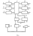
- Fig. US1, US2, US3 denote three synchronising units, of the kind provided by the present invention, which receives 2.048 Mbit/s PCM flows coming through connections 1, 2 and 3from video- conference rooms.
- bidirectional connections 4, 5 and 6 the outgoing flows are lead to a time switching stage CT and synchronism and timing signals of stage CT are sent to synchronising units US1, US2, US3.
- CT is in turn connected with output interfaces IU1, IU2 and IU3 by connections 7, 8 and 9. Duly switched flows are then sent back to videoconference rooms through connections 10, 11 and 12.
- Control unit CC controls various room switching according to automatic criteria based on the sound level or according to request criteria coming from the people present.
- Speech switching unit CV sequentially receives through connection 13 speech channels coming from the rooms and detects the speaker channel whose sound level is prominent. This information, supplied through connection 14to control unit CC, allows switching operations provided by the automatic criterion to be carried out.
- the switching unit is completed by a diagnosis unit CD, which effects suitable checks on the operation and detects possible anomalies, both inside each block and in the data exchanger among individual blocks.
- the diagnosis unit is accessed by a keyboard KB and test results are displayed on monitor MO.
- An individual synchronising unit, e.g. US1 is depicted in the block diagram of Fig. 2.
- connection 1a carries incoming wide-band data flow
- connection 1 incoming data timing and connection 1c frame synchronisation, consisting of a signal present for the whole duration of PCM frame of type A.
- Connection 4a carries the outgoing data flow to be sent to the switching stage, and connections 4b and 4c carry outgoing data timing and synchronism; the last two signals are supplied by the switching stage.
- Timing signals, present on wire 1b, and synchronism signals, present on wire 1c access a frequency divider DA, which determines the channel sequence of each frame, supplying at the output on wires 15 and 16 signals indicated if the channel number present at that instant is odd or even and on connection 17 the very number of the channel and frame (frame A or B) it belongs to.
- a frequency divider DA which determines the channel sequence of each frame, supplying at the output on wires 15 and 16 signals indicated if the channel number present at that instant is odd or even and on connection 17 the very number of the channel and frame (frame A or B) it belongs to.
- Complete reception of data belonging to a channel is signalled on wire 18, the frame beginning on wire 30 and received data availability on wire 31.
- Analogously frequency divider DB supplies on wires 19 and 20 signals indicating if the channel number to present at the output is odd or even, on wires 42 and 43 the command of blocks TA and TB and on connection 21 the very number of the channel, obtaining said information from signals coming from the switching stage over wires 4b and 4c.
- timing signals necessary to the operation of a logic circuit LC are sent over connection 22 and wire 34.
- References RA and RB denote two registers capable of alternately storing the contents of an incoming channel overwire 1a, upon command of the signals present on the already described wires 15 and 16, respectively.
- MA denotes a multiplexer apt to extract the data supplied by register RA or RB, upon command of the signals present on wires 15 and 16.
- MA is enabled to extract data by a signal supplied by logic circuit LC through wire 25.
- MB denotes a multiplexer apt to extract the numbers of incoming or outgoing channels supplied by frequency divider DA or DB, upon command of the switching signal coming from logic circuit LC through wire 26.
- MA supplies on wire 23 input data for a random-access memory RAM, and MB supplies on wire 24 the channel numbers, used as writing and reading addresses for memory RAM, apt to memorise two PCM frames.
- This memory is subdivided into two parts, each consisting of 32 octets and assigned to the storage of data belonging to frame A or frame B. Reading and writing operations are effected upon command of the logic circuit LC through wires 27, 28, 32 and 33.
- connection 29 Data outgoing on connection 29 are sent to two registers TA and TB, alternately controlled through wires 19,20,42,43 coming from frequency divider DB. Data outgoing from TAorTB are finally sent to the switching stage through connection 4a.
- Logic circuit LC is represented in more details on the block diagram of Fig. 3.
- LC comprises two different circuits, the one at the top is designed to identify the time phase in which the writing operations of the octets of the incoming channels and writing operations of the octets of the outgoing channels are to be effected, the circuit at the bottom supplies the data on the part of the memory where writing or reading are to be carried out.
- frequency divider DA sends a signal on wire 18. This signal, which indicates the octet reception end, is stored in a register FR, in this way circuit LC is informed that the arriving octet has been completely written in register RA or RB.
- the octet can then be stored in memory RAM at the channel address received through connection 24 and multiplexer MB from frequency divider DA, controlled by input signals 1b and 1c. These signals, in phase with input PCM frame, allow frequency divider DA to detect inside the frame the time position of the octet to be stored. This position is expressed as a binary number, used as an address of memory RAM where the octet is to be stored.
- the octet can be transferred to memory RAM, when enabled to writing by the signal on wire 32, received through gate P1 from frequency divider DA on wire 31.
- the memory part where the writing is to be effected is determined by a register FL, which stores through a signal on wire 30 the logic state present on wire 1c. A signal, whose logic level identifies either part of memory RAM, is then available at the output, connected to wire 28. As to the reading, it is always effected in the part of memory other than that where the writing is in progress.
- connection 21 The reading of an output channel octet to be stored in registers TA or TB, is determined by frequency divider DB by connection 21, and timing signals present on connection 22.
- This connection comprises three wires 22a, 22b and 22c, traversed by pulses at a frequency which is twice as high as the channel frequency and with suitable phase relations.
- the information previously stored in FR is transferred through wire 50 and gate P4, during the time phase in which the signal on wire 22a is at high logic value, to a register FC.
- the signal outgoing from FC on wire 26 determines the positioning of multiplexer MB to extract channel numbers supplied by DB.
- FC inhibits multiplexer MA and by the signal sent through gate P3 on wire 27 enables data output from the memory.
- P3 is controlled by the signal on wire 22b.
- the signal on wire 22c and through gate P2 controlled by the signal outgoing from register FC, the two registers FR and FC are then reset and can start the subsequent reading and writing cycle.
- the signal over wire 33 outgoing from a register FS, the part of the memory where reading operations are effected, is detected.
- FS is controlled by the signal present on wire 34, which carries the indication of the beginning of the outgoing frame, supplied by the switching stage and by the signal present on wire 28, already described.
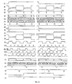
- FIG. 4 shows the waveforms of the signals present at the main points of the block diagrams of Figures 2 and 3.
- Each waveform is denoted by the same number as that of the wire on which it appears. More particularly:
Landscapes
- Engineering & Computer Science (AREA)
- Signal Processing (AREA)
- Multimedia (AREA)
- Computer Hardware Design (AREA)
- Computer Networks & Wireless Communication (AREA)
- Time-Division Multiplex Systems (AREA)
- Synchronisation In Digital Transmission Systems (AREA)
Claims (5)
Applications Claiming Priority (2)
| Application Number | Priority Date | Filing Date | Title |
|---|---|---|---|
| IT6820183 | 1983-11-17 | ||
| IT68201/83A IT1159627B (it) | 1983-11-17 | 1983-11-17 | Unita di sincronizzazione di trama pcm |
Publications (3)
| Publication Number | Publication Date |
|---|---|
| EP0144835A2 EP0144835A2 (de) | 1985-06-19 |
| EP0144835A3 EP0144835A3 (en) | 1986-03-26 |
| EP0144835B1 true EP0144835B1 (de) | 1988-08-17 |
Family
ID=11308462
Family Applications (1)
| Application Number | Title | Priority Date | Filing Date |
|---|---|---|---|
| EP84113843A Expired EP0144835B1 (de) | 1983-11-17 | 1984-11-15 | PCM-Rahmensynchronisierungseinheit |
Country Status (5)
| Country | Link |
|---|---|
| US (1) | US4723240A (de) |
| EP (1) | EP0144835B1 (de) |
| CA (1) | CA1255822A (de) |
| DE (2) | DE144835T1 (de) |
| IT (1) | IT1159627B (de) |
Families Citing this family (2)
| Publication number | Priority date | Publication date | Assignee | Title |
|---|---|---|---|---|
| US5420856A (en) * | 1991-06-18 | 1995-05-30 | Multimedia Design, Inc. | High-speed multi-media switching system |
| JP3033550B2 (ja) * | 1998-01-13 | 2000-04-17 | 三菱電機株式会社 | Scsiインタフェース接続装置、scsiコントローラ、scsiケーブル及びscsiバックプレーン |
Family Cites Families (6)
| Publication number | Priority date | Publication date | Assignee | Title |
|---|---|---|---|---|
| US3594502A (en) * | 1968-12-04 | 1971-07-20 | Itt | A rapid frame synchronization system |
| FR2312904A1 (fr) * | 1975-05-27 | 1976-12-24 | Poirier Alain | Perfectionnements aux systemes et aux dispositifs de teleconference par visiophonie |
| IT1159938B (it) * | 1978-10-18 | 1987-03-04 | Sits Soc It Telecom Siemens | Memoria elastica per demultiplatore sincrono di particolare applicazione nei sistemi di trasmissione a divisione di tempo |
| US4301534A (en) * | 1979-04-09 | 1981-11-17 | Digital Switch Corporation | Framing circuit for time multiplexed data |
| US4429386A (en) * | 1981-01-05 | 1984-01-31 | Siemens Corporation | Buffer arrangement of a PCM exchange system |
| FR2524750A1 (fr) * | 1982-03-30 | 1983-10-07 | Telecommunications Sa | Systeme de visioconference multisalle |
-
1983
- 1983-11-17 IT IT68201/83A patent/IT1159627B/it active
-
1984
- 1984-11-07 CA CA000467257A patent/CA1255822A/en not_active Expired
- 1984-11-15 DE DE198484113843T patent/DE144835T1/de active Pending
- 1984-11-15 DE DE8484113843T patent/DE3473543D1/de not_active Expired
- 1984-11-15 EP EP84113843A patent/EP0144835B1/de not_active Expired
-
1987
- 1987-02-17 US US07/017,030 patent/US4723240A/en not_active Expired - Fee Related
Also Published As
| Publication number | Publication date |
|---|---|
| DE3473543D1 (en) | 1988-09-22 |
| EP0144835A2 (de) | 1985-06-19 |
| EP0144835A3 (en) | 1986-03-26 |
| CA1255822A (en) | 1989-06-13 |
| US4723240A (en) | 1988-02-02 |
| IT8368201A0 (it) | 1983-11-17 |
| IT1159627B (it) | 1987-03-04 |
| DE144835T1 (de) | 1986-09-25 |
Similar Documents
| Publication | Publication Date | Title |
|---|---|---|
| US4322844A (en) | Transmitter-receiver synchronizer | |
| JPS58501799A (ja) | 電話交換制御装置 | |
| EP0249281B1 (de) | Fernsehbildwiedergabevorrichtung | |
| US4719510A (en) | Teletext decoders | |
| US4723240A (en) | PCM-frame synchronizing unit | |
| US4991013A (en) | Picture-in-picture television apparatus with sync controlled memory addressing | |
| JPS6248955B2 (de) | ||
| CA1225746A (en) | Error correction system for difference set cyclic code in a teletext system | |
| US3969587A (en) | Selective transmission of prerecorded voice signals to subscribers of time-sharing telecommunication system | |
| US5475706A (en) | Bulk data transmission system | |
| US5379298A (en) | Multimedia multiplexer device having automatic parameter recognizing and setting function, and communications systems including multimedia multiplexer devices | |
| US5629939A (en) | Time slot rearranging apparatus in multiplexer | |
| US3997874A (en) | Time divided switching and concentration apparatus | |
| JPS5911231B2 (ja) | テレビジヨン画像の伝送方式 | |
| US3963871A (en) | Analysis device for establishing the binary value of asynchronous data signals | |
| EP0048129A1 (de) | Digitaler Konzentrator | |
| US5657247A (en) | Method of playing back a sequence of images, in particular an animated sequence, as received successively in digitized form from a remote source, and corresponding apparatus | |
| JP3078183B2 (ja) | データ受信装置 | |
| JPH0380384B2 (de) | ||
| US5121392A (en) | Synchronous to non-synchronous data line pair interface apparatus | |
| JPH022360B2 (de) | ||
| GB2061673A (en) | Transmitter-receiver synchronizer | |
| GB1585028A (en) | Colour television systems | |
| JPS6013634B2 (ja) | 多重化情報信号受信装置 | |
| JP3655159B2 (ja) | 表示装置 |
Legal Events
| Date | Code | Title | Description |
|---|---|---|---|
| PUAI | Public reference made under article 153(3) epc to a published international application that has entered the european phase |
Free format text: ORIGINAL CODE: 0009012 |
|
| AK | Designated contracting states |
Designated state(s): DE FR GB NL SE |
|
| PUAL | Search report despatched |
Free format text: ORIGINAL CODE: 0009013 |
|
| AK | Designated contracting states |
Kind code of ref document: A3 Designated state(s): DE FR GB NL SE |
|
| 17P | Request for examination filed |
Effective date: 19860324 |
|
| EL | Fr: translation of claims filed | ||
| DET | De: translation of patent claims | ||
| 17Q | First examination report despatched |
Effective date: 19870520 |
|
| GRAA | (expected) grant |
Free format text: ORIGINAL CODE: 0009210 |
|
| AK | Designated contracting states |
Kind code of ref document: B1 Designated state(s): DE FR GB NL SE |
|
| REF | Corresponds to: |
Ref document number: 3473543 Country of ref document: DE Date of ref document: 19880922 |
|
| ET | Fr: translation filed | ||
| PLBE | No opposition filed within time limit |
Free format text: ORIGINAL CODE: 0009261 |
|
| STAA | Information on the status of an ep patent application or granted ep patent |
Free format text: STATUS: NO OPPOSITION FILED WITHIN TIME LIMIT |
|
| 26N | No opposition filed | ||
| PGFP | Annual fee paid to national office [announced via postgrant information from national office to epo] |
Ref country code: SE Payment date: 19941031 Year of fee payment: 11 |
|
| PGFP | Annual fee paid to national office [announced via postgrant information from national office to epo] |
Ref country code: GB Payment date: 19941107 Year of fee payment: 11 |
|
| PGFP | Annual fee paid to national office [announced via postgrant information from national office to epo] |
Ref country code: FR Payment date: 19941129 Year of fee payment: 11 |
|
| PGFP | Annual fee paid to national office [announced via postgrant information from national office to epo] |
Ref country code: NL Payment date: 19941130 Year of fee payment: 11 |
|
| EAL | Se: european patent in force in sweden |
Ref document number: 84113843.1 |
|
| PGFP | Annual fee paid to national office [announced via postgrant information from national office to epo] |
Ref country code: DE Payment date: 19950131 Year of fee payment: 11 |
|
| PG25 | Lapsed in a contracting state [announced via postgrant information from national office to epo] |
Ref country code: GB Effective date: 19951115 |
|
| PG25 | Lapsed in a contracting state [announced via postgrant information from national office to epo] |
Ref country code: SE Effective date: 19951116 |
|
| PG25 | Lapsed in a contracting state [announced via postgrant information from national office to epo] |
Ref country code: NL Effective date: 19960601 |
|
| GBPC | Gb: european patent ceased through non-payment of renewal fee |
Effective date: 19951115 |
|
| PG25 | Lapsed in a contracting state [announced via postgrant information from national office to epo] |
Ref country code: FR Effective date: 19960731 |
|
| NLV4 | Nl: lapsed or anulled due to non-payment of the annual fee |
Effective date: 19960601 |
|
| PG25 | Lapsed in a contracting state [announced via postgrant information from national office to epo] |
Ref country code: DE Effective date: 19960801 |
|
| EUG | Se: european patent has lapsed |
Ref document number: 84113843.1 |
|
| REG | Reference to a national code |
Ref country code: FR Ref legal event code: ST |