EP0143469A2 - Empfangsgerät für ein Rundfunkübertragungssystem - Google Patents
Empfangsgerät für ein Rundfunkübertragungssystem Download PDFInfo
- Publication number
- EP0143469A2 EP0143469A2 EP84114523A EP84114523A EP0143469A2 EP 0143469 A2 EP0143469 A2 EP 0143469A2 EP 84114523 A EP84114523 A EP 84114523A EP 84114523 A EP84114523 A EP 84114523A EP 0143469 A2 EP0143469 A2 EP 0143469A2
- Authority
- EP
- European Patent Office
- Prior art keywords
- carrier
- signal
- phase
- synchronous detection
- receiver unit
- Prior art date
- Legal status (The legal status is an assumption and is not a legal conclusion. Google has not performed a legal analysis and makes no representation as to the accuracy of the status listed.)
- Granted
Links
Images


Classifications
-
- H—ELECTRICITY
- H04—ELECTRIC COMMUNICATION TECHNIQUE
- H04L—TRANSMISSION OF DIGITAL INFORMATION, e.g. TELEGRAPHIC COMMUNICATION
- H04L27/00—Modulated-carrier systems
- H04L27/02—Amplitude-modulated carrier systems, e.g. using on-off keying; Single sideband or vestigial sideband modulation
- H04L27/06—Demodulator circuits; Receiver circuits
-
- H—ELECTRICITY
- H04—ELECTRIC COMMUNICATION TECHNIQUE
- H04L—TRANSMISSION OF DIGITAL INFORMATION, e.g. TELEGRAPHIC COMMUNICATION
- H04L27/00—Modulated-carrier systems
- H04L27/32—Carrier systems characterised by combinations of two or more of the types covered by groups H04L27/02, H04L27/10, H04L27/18 or H04L27/26
- H04L27/34—Amplitude- and phase-modulated carrier systems, e.g. quadrature-amplitude modulated carrier systems
- H04L27/38—Demodulator circuits; Receiver circuits
- H04L27/3818—Demodulator circuits; Receiver circuits using coherent demodulation, i.e. using one or more nominally phase synchronous carriers
-
- H—ELECTRICITY
- H04—ELECTRIC COMMUNICATION TECHNIQUE
- H04L—TRANSMISSION OF DIGITAL INFORMATION, e.g. TELEGRAPHIC COMMUNICATION
- H04L27/00—Modulated-carrier systems
Definitions
- the present invention relates to receiver unit for a radio communication system, and to such a system, and is applicable to a receiver unit having a carrier recovery circuit which recovers a leakage carrier included in a received multilevel quadrature amplitude modulation (QAM) signal and synchronously detects the leakage carrier with a reference carrier.
- QAM quadrature amplitude modulation
- a carrier is digitally modulated in accordance with data to be transmitted.
- modulation methods in practical use for such a digital radio communication system is the QAM method.
- a carrier is modulated in amplitude in accordance with data to be transmitted.
- the data is thereby transmitted as one of many corresponding coded points arranged on an imaginary plane defined by an in-phase (I) axis and a quadrature (Q) axis. This enables a large amount of data to be transmitted at one time and thus significantly increases the transmission capacity of a radio transmission line.
- the carrier contained in the received multilevel QAM signal is recovered and divided into two route signals forming I- and Q-channel data signals having a quadrature relationship so as to synchronously detect the quadrature multilevel QAM data signals with carriers having a quadrature relationship. Both synchronous detected data signals are amplitude- discriminated, then the transmitted digital data are demodulated. In order to ensure precise demodulation of the transmitted data signal in the receiver unit, provision of an accurate carrier for synchronous detection of the received multilevel QAM signal is essential.
- the carrier is suppressed in the transmission data signal. It is, however, difficult to extract the carrier in the receiver unit. A great deal of circuit elements are required for suitably recovering the carrier.
- the most frequently used multilevel QAM method in the prior art is the 16-value method.
- a typical 4-phase phase shift keying (PSK) method or Costas loop application method are utilized for recovering the carrier.
- PSK 4-phase phase shift keying
- Costas loop application method are utilized for recovering the carrier.
- phase selection control process in the carrier recovery circuit for realizing the process.
- the prior art carrier recovery circuit cannot suppress phase fluctuation, i.e., "jitter" of the carrier, which adversely affects the synchronous detection.
- a radio communication system wherein the transmitter unit adds a DC offset to either an I-channel or Q-channel data signal to be transmitted so as to include a leakage carrier.
- the receiver unit receives the transmission data including the leakage carrier, extracts the leakage carrier, and controls the phase of the leakage carrier to synchronize with the phase of the reference carrier (See "Radio Communication System", U.S. Serial No. 566,401, filed on Dec. 28, 1983 or EPC Application No. 83307949.4, filed on Dec. 23, 1983 or Korea Application No. 83-6248, filed on Dec. 28, 1983).
- An object of the present invention is to provide a receiver unit having a carrier recovery circuit in a multilevel QAM, preferably a 16-, 32-, 64-, or higher level QAM method radio communication system, which can eliminate jitter of the carrier.
- Another object of the present invention is to provide a receiver unit having a carrier recovery circuit in a radio communication system which can easily discriminate received multilevel QAM data signals to ensure obtainment of a fully opened eye pattern.
- Still another object of the present invention is to provide a receiver unit having a carrier recovery circuit which can facilitate the extraction of a carrier with a simple circuit construction.
- a receiver unit for a radio communication system in which a transmitter unit outputs transmission data, modulated in accordance with a multilevel QAM method and containing a leakage carrier by addition of a DC offset signal to either one of the quadrature components forming the transmission data, to the receiver unit through a transmission line, including: means for receiving transmission data; means for branching a signal received at the transmission data receiving means into first and second signal components forming the multilevel QAM data, each including the leakage carrier having a phase difference of ; radian, first channel means for demodulating the first branched signal component and including a first synchronous detection circuit and a first discriminator; second channel means for demodulating the second branched signal component and including a second synchronous detection circuit and a first discriminator; and means for recovering the carrier, including a control circuit, for cancelling a noise component contained in the output signal from either one of the first and second synchronous detection circuits and for providing only a DC component representing a phase difference between a leakage
- the means for recovering the carrier includes a control circuit, for extracting a signal responsive to a phase difference between inputs and outputs of the first and second discriminators, for summing the extracted signal and an output signal at either one of the first and second synchronous detection circuits, and for providing only a DC component including the phase difference component, and a PLL circuit, for controlling the phase difference to zero and for providing phase-locked leakage carriers to the reference carriers, having a phase difference of 2 radian, to the first and second synchronous detection circuits.
- a control circuit for extracting a signal responsive to a phase difference between inputs and outputs of the first and second discriminators, for summing the extracted signal and an output signal at either one of the first and second synchronous detection circuits, and for providing only a DC component including the phase difference component
- a PLL circuit for controlling the phase difference to zero and for providing phase-locked leakage carriers to the reference carriers, having a phase difference of 2 radian, to the first and second synchronous detection circuits.
- a similar receiver unit where means for recovering the carrier includes a control circuit, for extracting only the leakage carrier component due to _the DC offset, and a PLL circuit, for achieving synchronization of the leakage carrier with a reference carrier and for providing phase-locked leakage carriers to the reference carriers, having a phase difference of radian, to the first and second synchronous detection circuits.
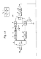
- FIG. 1 is a block diagram of an embodiment of a radio communication system in accordance with the present invention.
- the radio communication system includes a transmitter unit 100, a transmission line 150, and a receiver unit 200.
- the transmitter unit 100 includes a serial-to- parallel (S/P) converter 1 for converting serial digital input data D in , coded by, for example, pulse-code modulation (PCM), to a parallel signal, and a multilevel converter (ML CONV) 2 specifically formed by a digital-to-analog (D/A) converter and for transforming the parallel data from the S/P converter to an analog data signal.
- S/P serial-to- parallel
- ML CONV multilevel converter
- D/A digital-to-analog
- One of the two route signals is the so-called I-channel data signal DI, and the other is the Q-channel data signal DQ.
- the transmitter unit 100 includes a low-pass filter 3, a high-pass filter 5, an adder 7, a DC offset source 8, and a modulator 9 in the I-channel, and includes a low-pass filter 4, a high-pass filter 6, and a modulator 10 in the Q-channel.
- the low-pass filters 3 and 4 are identical and perform band-pass limitation and wave-shaping for the I- and Q-channel signals DI and DQ.
- the high-pass filters 5 and 6 are identical and reduce amplitudes of the low-pass filtered signals on a carrier frequency f 0 to predetermined amplitudes. The reduction of the amplitude will be explained later.
- the high-pass filtered I-channel signal is added the offset voltage V off from the DC offset source 8 cooperating therewith at the adder 7.
- the output from the adder 7 is applied to the modulator 9.
- the output from the high-pass filter 6 is applied to the modulator 10.
- a carrier CR having a center frequency f 0 is given, on one hand, to the modulator 10 directly and, on the other hand, to the modulator 9 via a ⁇ /2 (90°) phase shifter 11.
- a modulation operation is performed to the I-channel data signal biased by the offset voltage off and the Q-channel data signal with the carrier CR at the modulators 9 and 10.
- the transmitter unit 100 further includes a hybrid circuit (H) 12, an intermediate frequency amplifier 13, and a band-pass filter 14.
- H hybrid circuit
- the modulated signal is then amplified at the amplifier 13 and the desired transmission frequency band signal component is chosen by the filter 14.
- the filtered signal is further amplified up to a predetermined transmission level by means of a high power transmission amplifier (not shown).
- the multilevel QAM modulated and amplified signal is transmitted from the transmitter unit 100, via the transmission line 150, to the receiver unit 200.
- the multilevel data of the I-channel and the Q-channel consists of a six-bit signal of binary data, consequently, binary six-bit data, which can represent up to 64 values, can be transmitted at one time.
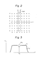
- Figure 2 is a schematic pattern view of the distribution of coded points of I-channel data and Q-channel data, taking the case of a 64-level QAM method as an example.
- the ordinate I represents the I-channel
- the abscissa Q' the Q-channel when the offset value V off is not added to the I channel data at the adder 7.
- the abscissa Q represents the Q-channel shifted by the offset value V off from the Q axis when the offset value V off is forcibly added to the I-channel data signal, as mentioned above.
- Each channel has eight coded points.
- Cross points in the I and Q axes indicate the eight (8)-value amplitude coded points by means of the multilevel I channel data and the multilevel Q-channel data, respectively. Therefore each of the 64 signal components shown as black points in a matrix pattern is defined by vector synthesis with the quadrature amplitude coded signals.
- the signal components of the right-side phase with respect to the shifted axis Q and the signal components of the left-side phase occur at an unbalanced ratio of 5:3, as shown in Fig. 2.
- Figure 3 is a graph of a spectrum of the transmission signal from the transmitter unit 100 shown in Fig. 1.
- the ordinate f represents frequency, and the abscissa V voltage.
- the multilevel QAM transmission signal which does not include the leakage carrier, exhibits a flat characteristic at the middle of the spectrum, as illustrated by a broken curve C 1 . Therefore, no leakage carrier can be observed.
- the leakage carrier CR L stands at the middle of the spectrum.
- a V-shaped recess in the vicinity of the carrier frequency f 0 on a curve C 2 is formed by the high-pass filters 5 and 6 in the transmitter unit 100 to save the power consumption in the radio communication system, because the top level of the carrier CR L standing on the curve C 2 is reduced more than that standing on the curve C, , and to facilitate the extraction of the carrier CR in the receiver unit 200 because the carrier CR L separately stands from the adjacent portions.
- the receiver unit 200 includes a hybrid circuit 21 for branching the received multilevel QAM signal into two route signals forming I-channel and Q-channel data signals.
- the receiver unit 200 includes a synchronous detector 22, an amplifier 24, a low-pass filter 26, and a discriminator 28 for the I-channel.
- the receiver unit 200 also includes a synchronous detector 23, an amplifier 25, a low-pass filter 27, and a discriminator 29 for the Q-channel.
- the receiver unit 200 includes a bit timing recovery circuit 45 for providing a clock signal used in the discriminators 28 and 29.
- the discriminators 28 and 29 are analog-to- digital (A/D) converters in this embodiment.
- the receiver unit 200 includes a parallel-to serial (P/S) data converter 30.
- the receiver unit 200 further includes a carrier recovery circuit consisting of a hybrid circuit 46, a mixer 47, a low-pass filter 48, voltage-controlled oscillator 49, a variable phase shifter 50, and a ⁇ /2 (90°) phase shifter 51.
- a carrier recovery circuit consisting of a hybrid circuit 46, a mixer 47, a low-pass filter 48, voltage-controlled oscillator 49, a variable phase shifter 50, and a ⁇ /2 (90°) phase shifter 51.
- the receiver unit 200 includes transmission data receiving means consisting of an antenna, a down converter, etc. (not shown).
- the received multilevel QAM signal is branched into an I-channel data signal DI r and a Q-channel data signal DQ at the hybrid circuit 21.
- the I-channel and Q-channel data signals DI r and DQ are applied to the synchronous detection circuit 22 and 23 and are synchronous-detected with reference carriers CR' and CR" extracted at the carrier recovery circuit 210 and having a phase difference of ; radian. The extraction of the carrier CR' will be explained later.
- I-channel and Q-channel synchronous detected output signals from the circuit 22 and 23 are amplified at the amplifiers 24 and 25 and are applied to the discriminators 28 and 29 through the low-pass filters 26 and 27.
- the bit timing recovery circuit 20 picks up a clock signal contained in the I-channel multilevel QAM signal and generally placed out of the inherent data band and generates a clock signal for driving the discriminators 28 and 29.
- the discriminators 28 and 29 are A/D converters in this embodiment. Therefore, the I-channel and Q-channel data signals applied to the A/D converters 28 and 29 are converted into three-bit I-channel and Q-channel data signals, respectively.
- the parallel three-bit I-channel and Q-channel data signals are converted into six-bit serial data, which may be indenti- cal to the input data D in in the transmitter unit 100.
- a certain level signal may appear on, for example, the Q-channel multilevel data signal output from the synchronous detection circuit 23 at a point Pl, in response to both a frequency difference and a phase difference between the leakage carrier, which will be recovered at the carrier recovery circuit, and the reference carrier, which may be used at the synchronous detection circuit 23.
- the carrier recovery circuit 210 is operable to synchronize the phase of the output signal from the voltage-controlled oscillator 33, i.e., the phase of the recovered carrier, to the phase of the reference carrier.
- the modulated transmission signal f 0 (t) of the transmission unit 100 is expressed as below: where, x(t): I-channel multilevel data, y(t): Q-channel multilevel data, ⁇ : Angular frequency.
- the first expression [V off + X(t)]sin ⁇ represents the component of the I-channel data signal DI
- the second expression (t)cos ⁇ represents the component of the Q-channel data signal DQ.
- the low-pass filter 48 can also eliminate the signal components of X(t) and y(t). Then, only the output V off ⁇ sin ⁇ , which is a leakage component, is obtained from the filter 48.
- the V off ⁇ sin ⁇ component can be reduced to zero, in other words, the phase difference ⁇ can be reduced to zero, when the leakage carrier component sin(wt + ⁇ ) becomes in phase with the reference carrier component sin wt.
- the output V off ⁇ sin ⁇ from the low-pass filter 48 is supplied to a control terminal of the voltage-controlled oscillator 49.
- the output of the oscillator 49 is supplied to both the mixer 47 and the phase shifter 50.
- the output of the phase shifter 50 is applied to the synchronous detector 23 and to the synchronous detector 22 via the phase shifter 51.
- the carrier recovery circuit 210 mentioned above operates as a PLL circuit under control of the DC component V off ⁇ sin ⁇ as such to reduce it to zero.
- the synchronous detection circuits 22 and 23 are operable to synchronously detect the I-channel and Q-channel data signals DI and DQ r with the reference carriers CR" and CR' being in-phase to the leakage carrier and having a phase difference of radian. This ensures high accuracy synchronous detection of the multilevel QAM data and enables high reproductivity of the transmitted higher order multilevel QAM data.
- the carrier recovery circuit 210 in Fig. 1 is somewhat complex. A simpler circuit was devised, however, the principal philosophy mentioned above stands throughout the present invention.
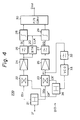
- FIG. 4 is a block diagram of another embodiment of the receiver unit 200.
- the circuit elements 20 to 30 are identical to those in Fig. 1.
- the carrier recovery circuit in Fig. 4, bearing reference numeral 210 differs from that in Fig. 1.
- the carrier recovery circuit 210 in Fig. 4 includes a low-pass filter 32, a voltage-controlled oscillator 33, and a ; (90°) hybrid circuit 34.
- the carrier recovery circuit 210 in Fig. 4 is simpler than that in Fi g . 1, because the mixer 47 and the phase shifter 50 of Fig. 1 are omitted.
- the hybrid circuit 34 operates similar to the phase shifter 51 in Fig. 1, accordingly the hybrid circuit 34 can be replaced by the phase shifter 51.
- the low-pass filter 32 and the voltage-controlled oscillator 33 are similar to the corresponding elements 48 and 49, respectively.
- circuit elements 20 to 30 operate the same as in the above-mentioned embodiment.
- the output signal from the synchronous detection circuit 23, at the point Pl can be expressed as in equation (3), mentioned above.
- the output signal at the point Pl is applied to the low-pass filter 32 so as to pass only the DC component V off ⁇ sin ⁇ within the leakage carrier component.
- the DC component is applied to the control terminal of the voltage-controlled oscillator 33, whereby the output phase of the voltage-controlled oscillator 33 is controlled so as to make the phase difference 6 between the reference and the leakage carriers zero.
- the carriers CR' and CR" phase-controlled through the hybrid circuit 34, having a phase difference, are applied to the synchronous detection circuit 22 and 23. Accordingly, high accuracy synchronous detection is achieved in the synchronous detection circuits 22 and 23, ensuring high quality demodulation of the received multilevel QAM data signal.
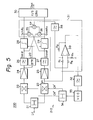
- FIG. 5 is a block diagram of still another embodiment of the receiver unit 200.
- the circuit elements 20 to 30 are identical to those in Fig. 1.
- the carrier recovery circuit 210 includes a phase control circuit 31, a low-pass filter 32, a voltage-controlled oscillator 33, and a ; hybrid circuit 34.
- the filter 32, the oscillator 33, and the hybrid circuit 34 are identical to the corresponding circuit elements 32, 33 and 34 in Fig. 4.
- the phase control circuit 30 includes multipliers 35 and 36, a divider 37, a low-pass filter 38, and an amplifier circuit consisting of an operational amplifier 39 and resistors R1 to R4.
- the signal from the synchronous detection circuit 23, which is expressed by equation (3), is added to an inverted terminal of the amplifier 39.
- the component sin( ⁇ - ⁇ 0 ) from the low-pass filter 38 is added to a non-inverted terminal at the amplifier 39.
- the deviation output from the amplifier 39 is applied to the low-pass filter 32 to extract the DC component V off ⁇ sin( ⁇ - ⁇ 0 ).
- the voltage-controlled oscillator 33 receives the DC component at its control input and controls the phase to synchronize the leakage carrier with the reference carrier and to make the component sin( ⁇ - ⁇ 0 ) zero. Accordingly, an optimum carrier can be recovered and the eye pattern for the input signal to the discriminators 28 and 29 can be fully opened simultaneously. This results in high quality discrimination at the discriminators 28 and 29 as well as high stability synchronous detection at the synchronous detection circuits 22 and 23 simultaneously.
- FIG. 6 is a block diagram of another embodiment of the receiver unit 200.
- the circuit elements 20 to 30 are identical to those in Fig. 1.
- the carrier recovery circuit 210 includes a phase control circuit 31 consisting of a D/A converter 40 and an adder 41; a low-pass filter 32; a voltage-controlled oscillator 33; and a ; hybrid circuit 34.
- the low-pass filter 32, the voltage-controlled oscillator 33, and the hybrid circuit 34 are similar to the corresponding elements in Fig. 4.
- the signal output from the synchronous detection circuit 23 is expressed by equation (3). Accordingly, it includes the leakage carrier component and data component.
- the higher harmonic components contained in the above output signal can be eliminated by the low-pass filter 32, however, the noise component contained in the baseband signal component may still remain. The remaining noise component adversely affects suppression of the jitter of the carrier at the output of the voltage-controlled oscillator 33.
- This disadvantage may arise in the circuits in Figs. 1, 4, and 5. This disadvantage, however, can be solved by providing the phase control circuit 31 in Fig. 6, described below.
- the digital Q-channel signal from the discriminator 29 is applied to the D/A converter 40 and converted into an analog signal including the noise component contained in the baseband signal component.
- the signal output from the synchronous detection circuit 23 is subtracted by the signal from the D/A converter 40 so that the resultant signal at the output of the adder 41 does not include the noise component contained in the baseband signal component.
- the jitter of the carrier can be reduced to zero. This establishes high stability of synchronous detection at the synchronous detection circuits 22 and 23 so that high-quality demodulation of the received multilevel QAM signal is realized.
- the circuit construction in Fig. 6 is quite simple and has no expensive elements.
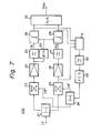
- Figure 7 is a block diagram of still another embodiment of the receiver unit 200.
- the circuit elements 20 to 30 are identical to those in Fig. 1.
- the circuit elements 32 to 34 are identical to those in Fig. 4.
- a phase control circuit 31 in Fig. 7 is formed by the combination of the phase control circuits shown in Figs. 4 to 6. Therefore, the receiver unit 200 in Fig. 7 performs as a combined receiver units in Figs. 4 to 6.
- phase control circuit 31 and the low-pass filter 32 forms a control circuit.
Landscapes
- Engineering & Computer Science (AREA)
- Computer Networks & Wireless Communication (AREA)
- Signal Processing (AREA)
- Digital Transmission Methods That Use Modulated Carrier Waves (AREA)
- Synchronisation In Digital Transmission Systems (AREA)
Applications Claiming Priority (2)
| Application Number | Priority Date | Filing Date | Title |
|---|---|---|---|
| JP58224441A JPH0714170B2 (ja) | 1983-11-30 | 1983-11-30 | 搬送波再生回路 |
| JP224441/83 | 1983-11-30 |
Publications (3)
| Publication Number | Publication Date |
|---|---|
| EP0143469A2 true EP0143469A2 (de) | 1985-06-05 |
| EP0143469A3 EP0143469A3 (en) | 1986-07-30 |
| EP0143469B1 EP0143469B1 (de) | 1989-05-31 |
Family
ID=16813816
Family Applications (1)
| Application Number | Title | Priority Date | Filing Date |
|---|---|---|---|
| EP84114523A Expired EP0143469B1 (de) | 1983-11-30 | 1984-11-30 | Empfangsgerät für ein Rundfunkübertragungssystem |
Country Status (6)
| Country | Link |
|---|---|
| US (1) | US4633484A (de) |
| EP (1) | EP0143469B1 (de) |
| JP (1) | JPH0714170B2 (de) |
| KR (1) | KR890002727B1 (de) |
| CA (1) | CA1238370A (de) |
| DE (1) | DE3478556D1 (de) |
Cited By (5)
| Publication number | Priority date | Publication date | Assignee | Title |
|---|---|---|---|---|
| GB2207582A (en) * | 1987-07-30 | 1989-02-01 | Stc Plc | Phase error correction and carrier recovery |
| GB2232852A (en) * | 1989-05-31 | 1990-12-19 | Technophone Ltd | Offset correction |
| FR2655788A1 (fr) * | 1989-12-11 | 1991-06-14 | France Etat | Systeme de transmission a modulation d'amplitude a porteuse supprimee, conservant la polarite du signal transmis. |
| EP0496408A1 (de) * | 1991-01-25 | 1992-07-29 | Samsung Electronics Co., Ltd. | Verfahren und Schaltungsanordnung zum Senden von Meldungen in einem Fahrzeugortungssystem |
| EP0493748A3 (en) * | 1990-12-24 | 1992-08-05 | Ant Nachrichtentechnik Gmbh | Method and circuit arrangement for determination of a control information for the quadrature phase in a qam receiver |
Families Citing this family (12)
| Publication number | Priority date | Publication date | Assignee | Title |
|---|---|---|---|---|
| JPS62142440A (ja) * | 1985-12-17 | 1987-06-25 | Fujitsu Ltd | 変復調装置 |
| US5040194A (en) * | 1986-07-15 | 1991-08-13 | Hayes Microcomputer Products, Inc. | Method and apparatus for providing for automatic gain control of incoming signals in a modem |
| FR2644638B1 (de) * | 1989-03-14 | 1991-05-31 | Labo Electronique Physique | |
| FR2649845B1 (fr) * | 1989-07-12 | 1994-05-13 | Alcatel Transmission Faisceaux H | Dispositif de reception pour faisceau hertzien numerique |
| GB8918431D0 (en) * | 1989-08-12 | 1989-09-20 | Lucas Ind Plc | Apparatus for aircraft flight |
| US5233634A (en) * | 1989-10-18 | 1993-08-03 | Nokia Mobile Phones Ltd. | Automatic gain control circuit in a radio telephone receiver |
| US5493581A (en) * | 1992-08-14 | 1996-02-20 | Harris Corporation | Digital down converter and method |
| US5786865A (en) * | 1996-06-28 | 1998-07-28 | Zilog, Inc. | Apparatus and method for digital amplitude and phase detection |
| US6433906B1 (en) * | 1999-09-22 | 2002-08-13 | Scientific-Atlanta, Inc. | Digital optical receiver for cable television systems |
| US7801250B2 (en) * | 2006-05-24 | 2010-09-21 | General Dynamics Advanced Information Systems, Inc. | Low latency analog QAM coherent demodulation algorithm |
| US7622987B1 (en) | 2007-01-25 | 2009-11-24 | Pmc-Sierra, Inc. | Pattern-based DC offset correction |
| US10979277B1 (en) * | 2019-12-31 | 2021-04-13 | Texas Instruments Incorporated | Carrier frequency recovery in a receiver |
Family Cites Families (12)
| Publication number | Priority date | Publication date | Assignee | Title |
|---|---|---|---|---|
| US3196352A (en) * | 1962-12-18 | 1965-07-20 | Ibm | Multilevel vestigial sideband suppressed carrier data transmission system |
| US3518680A (en) * | 1967-10-02 | 1970-06-30 | North American Rockwell | Carrier phase lock apparatus using correlation between received quadrature phase components |
| BE766847A (fr) * | 1971-05-07 | 1971-11-08 | Acec | Procede de transmission d'informations avec restitution automatique de l'onde porteuse dans le recepteur, |
| DE2245189C3 (de) * | 1971-09-18 | 1980-09-25 | Fujitsu Ltd., Kawasaki, Kanagawa (Japan) | Vorrichtung zur Übertragung eines restseitenbandträgermodulierten Mehrpegelsignals und eines Synchronisier-Pilotsignals |
| US3818347A (en) * | 1972-10-10 | 1974-06-18 | Intertel Inc | Receiver for amplitude modulated quadrature carrier signals |
| US3849730A (en) * | 1973-06-20 | 1974-11-19 | Bell Telephone Labor Inc | Carrier recovery in vestigial sideband data receivers |
| JPS50135909A (de) * | 1974-04-08 | 1975-10-28 | ||
| JPS5224410A (en) * | 1975-08-20 | 1977-02-23 | Fujitsu Ltd | Carrier wave regenerative circuit |
| US4355397A (en) * | 1980-10-15 | 1982-10-19 | Rixon, Inc. | Full duplex communication system for voice grade channels |
| US4358853A (en) * | 1981-01-22 | 1982-11-09 | Codex Corporation | Digital modem transmitter |
| US4470145A (en) * | 1982-07-26 | 1984-09-04 | Hughes Aircraft Company | Single sideband quadricorrelator |
| CA1217233A (en) * | 1982-12-29 | 1987-01-27 | Susumu Sasaki | Qam with dc bias in one channel |
-
1983
- 1983-11-30 JP JP58224441A patent/JPH0714170B2/ja not_active Expired - Lifetime
-
1984
- 1984-11-20 CA CA000468236A patent/CA1238370A/en not_active Expired
- 1984-11-23 US US06/674,314 patent/US4633484A/en not_active Expired - Fee Related
- 1984-11-29 KR KR1019840007501A patent/KR890002727B1/ko not_active Expired
- 1984-11-30 DE DE8484114523T patent/DE3478556D1/de not_active Expired
- 1984-11-30 EP EP84114523A patent/EP0143469B1/de not_active Expired
Cited By (10)
| Publication number | Priority date | Publication date | Assignee | Title |
|---|---|---|---|---|
| GB2207582A (en) * | 1987-07-30 | 1989-02-01 | Stc Plc | Phase error correction and carrier recovery |
| GB2207582B (en) * | 1987-07-30 | 1991-04-24 | Stc Plc | Phase error correction and carrier recovery |
| GB2232852A (en) * | 1989-05-31 | 1990-12-19 | Technophone Ltd | Offset correction |
| US5081652A (en) * | 1989-05-31 | 1992-01-14 | Technophone Ltd. | Offset correction |
| EP0400782A3 (de) * | 1989-05-31 | 1992-03-18 | Nokia Mobile Phones (U.K.) Limited | Verschiebungskorrektur |
| GB2232852B (en) * | 1989-05-31 | 1993-10-27 | Technophone Ltd | Offset correction |
| FR2655788A1 (fr) * | 1989-12-11 | 1991-06-14 | France Etat | Systeme de transmission a modulation d'amplitude a porteuse supprimee, conservant la polarite du signal transmis. |
| EP0433198A1 (de) * | 1989-12-11 | 1991-06-19 | France Telecom | Amplitudenmodulation-Übertragungssystem mit unterdrÀ¼cktem Träger, das die Polarität des übertragenen Signals erhält |
| EP0493748A3 (en) * | 1990-12-24 | 1992-08-05 | Ant Nachrichtentechnik Gmbh | Method and circuit arrangement for determination of a control information for the quadrature phase in a qam receiver |
| EP0496408A1 (de) * | 1991-01-25 | 1992-07-29 | Samsung Electronics Co., Ltd. | Verfahren und Schaltungsanordnung zum Senden von Meldungen in einem Fahrzeugortungssystem |
Also Published As
| Publication number | Publication date |
|---|---|
| EP0143469B1 (de) | 1989-05-31 |
| JPS60117946A (ja) | 1985-06-25 |
| EP0143469A3 (en) | 1986-07-30 |
| JPH0714170B2 (ja) | 1995-02-15 |
| KR890002727B1 (ko) | 1989-07-25 |
| CA1238370A (en) | 1988-06-21 |
| US4633484A (en) | 1986-12-30 |
| DE3478556D1 (en) | 1989-07-06 |
| KR850005189A (ko) | 1985-08-21 |
Similar Documents
| Publication | Publication Date | Title |
|---|---|---|
| EP0143469B1 (de) | Empfangsgerät für ein Rundfunkübertragungssystem | |
| FI80175C (fi) | Digitalt telekommunikationssystem, daer anvaends kvadraturmodulerade baervaogssignaler. | |
| EP0772905B1 (de) | Direktmischempfänger | |
| US4509017A (en) | Method and apparatus for pulse angle modulation | |
| EP0135377A2 (de) | Modulator und Demodulator zur Verarbeitung von amplituden- und phasenumgetasteten Modulationssignalen | |
| US5402449A (en) | Process and device for converting digitally modulate high-frequency reception signals | |
| US5581582A (en) | Automatic frequency control method and apparatus therefor | |
| CA1303691C (en) | Carrier recovery phase-locked loop | |
| KR100459741B1 (ko) | M진fsk신호들복조방법,m진fsk심볼들수신및복조방법,m진fsk신호들복조기,m진fsk심볼들수신기 | |
| US5134634A (en) | Multilevel quadrature amplitude demodulator capable of compensating for a quadrature phase deviation of a carrier signal pair | |
| KR20010072039A (ko) | 직교 복조기에서의 미분 및 곱셈에 기반한 타이밍 회복 | |
| US4887280A (en) | System for detecting the presence of a signal of a particular data rate | |
| KR19980015790A (ko) | 직각 위상 편이 복조기의 자동 이득 제어장치 | |
| US20020126771A1 (en) | Demodulator for a radio receiver and method of operation | |
| US4674105A (en) | Digital signal processor | |
| EP0113246B1 (de) | Radio-Kommunikationssystem | |
| WO1999027689A2 (en) | Demodulation unit and method of demodulating a quadrature signal | |
| US6011816A (en) | Direct demodulation method and apparatus | |
| JPH0621992A (ja) | 復調器 | |
| US6707863B1 (en) | Baseband signal carrier recovery of a suppressed carrier modulation signal | |
| US5546428A (en) | Differentially encoding quadrature phase shift keying modulation method and apparatus thereof | |
| US4614910A (en) | Quarternary differential PSK demodulator | |
| US4186348A (en) | Receiver for data transmitted by means of the interleaved binary phase shift keyed modulation technique | |
| US7457375B2 (en) | Timing extractor, timing extraction method, and demodulator having the timing extractor | |
| JP2910695B2 (ja) | コスタスループ搬送波再生回路 |
Legal Events
| Date | Code | Title | Description |
|---|---|---|---|
| PUAI | Public reference made under article 153(3) epc to a published international application that has entered the european phase |
Free format text: ORIGINAL CODE: 0009012 |
|
| AK | Designated contracting states |
Designated state(s): DE FR GB IT NL SE |
|
| PUAL | Search report despatched |
Free format text: ORIGINAL CODE: 0009013 |
|
| AK | Designated contracting states |
Kind code of ref document: A3 Designated state(s): DE FR GB IT NL SE |
|
| 17P | Request for examination filed |
Effective date: 19860819 |
|
| 17Q | First examination report despatched |
Effective date: 19871210 |
|
| GRAA | (expected) grant |
Free format text: ORIGINAL CODE: 0009210 |
|
| AK | Designated contracting states |
Kind code of ref document: B1 Designated state(s): DE FR GB IT NL SE |
|
| REF | Corresponds to: |
Ref document number: 3478556 Country of ref document: DE Date of ref document: 19890706 |
|
| ITF | It: translation for a ep patent filed | ||
| ET | Fr: translation filed | ||
| PLBE | No opposition filed within time limit |
Free format text: ORIGINAL CODE: 0009261 |
|
| STAA | Information on the status of an ep patent application or granted ep patent |
Free format text: STATUS: NO OPPOSITION FILED WITHIN TIME LIMIT |
|
| 26N | No opposition filed | ||
| PGFP | Annual fee paid to national office [announced via postgrant information from national office to epo] |
Ref country code: GB Payment date: 19901002 Year of fee payment: 7 |
|
| PGFP | Annual fee paid to national office [announced via postgrant information from national office to epo] |
Ref country code: SE Payment date: 19901121 Year of fee payment: 7 |
|
| PGFP | Annual fee paid to national office [announced via postgrant information from national office to epo] |
Ref country code: FR Payment date: 19901129 Year of fee payment: 7 |
|
| ITTA | It: last paid annual fee | ||
| PGFP | Annual fee paid to national office [announced via postgrant information from national office to epo] |
Ref country code: NL Payment date: 19901130 Year of fee payment: 7 |
|
| PGFP | Annual fee paid to national office [announced via postgrant information from national office to epo] |
Ref country code: DE Payment date: 19901213 Year of fee payment: 7 |
|
| PG25 | Lapsed in a contracting state [announced via postgrant information from national office to epo] |
Ref country code: GB Effective date: 19911130 |
|
| PG25 | Lapsed in a contracting state [announced via postgrant information from national office to epo] |
Ref country code: SE Effective date: 19911201 |
|
| PG25 | Lapsed in a contracting state [announced via postgrant information from national office to epo] |
Ref country code: NL Effective date: 19920601 |
|
| NLV4 | Nl: lapsed or anulled due to non-payment of the annual fee | ||
| GBPC | Gb: european patent ceased through non-payment of renewal fee | ||
| PG25 | Lapsed in a contracting state [announced via postgrant information from national office to epo] |
Ref country code: FR Effective date: 19920731 |
|
| PG25 | Lapsed in a contracting state [announced via postgrant information from national office to epo] |
Ref country code: DE Effective date: 19920801 |
|
| REG | Reference to a national code |
Ref country code: FR Ref legal event code: ST |
|
| EUG | Se: european patent has lapsed |
Ref document number: 84114523.8 Effective date: 19920704 |