EP0141933A2 - Integrierbare Oszillatorschaltung - Google Patents
Integrierbare Oszillatorschaltung Download PDFInfo
- Publication number
- EP0141933A2 EP0141933A2 EP84109769A EP84109769A EP0141933A2 EP 0141933 A2 EP0141933 A2 EP 0141933A2 EP 84109769 A EP84109769 A EP 84109769A EP 84109769 A EP84109769 A EP 84109769A EP 0141933 A2 EP0141933 A2 EP 0141933A2
- Authority
- EP
- European Patent Office
- Prior art keywords
- transistor
- emitter
- collector
- base
- connection
- Prior art date
- Legal status (The legal status is an assumption and is not a legal conclusion. Google has not performed a legal analysis and makes no representation as to the accuracy of the status listed.)
- Granted
Links
Images


Classifications
-
- H—ELECTRICITY
- H03—ELECTRONIC CIRCUITRY
- H03B—GENERATION OF OSCILLATIONS, DIRECTLY OR BY FREQUENCY-CHANGING, BY CIRCUITS EMPLOYING ACTIVE ELEMENTS WHICH OPERATE IN A NON-SWITCHING MANNER; GENERATION OF NOISE BY SUCH CIRCUITS
- H03B5/00—Generation of oscillations using amplifier with regenerative feedback from output to input
- H03B5/30—Generation of oscillations using amplifier with regenerative feedback from output to input with frequency-determining element being electromechanical resonator
- H03B5/32—Generation of oscillations using amplifier with regenerative feedback from output to input with frequency-determining element being electromechanical resonator being a piezoelectric resonator
- H03B5/36—Generation of oscillations using amplifier with regenerative feedback from output to input with frequency-determining element being electromechanical resonator being a piezoelectric resonator active element in amplifier being semiconductor device
-
- H—ELECTRICITY
- H03—ELECTRONIC CIRCUITRY
- H03B—GENERATION OF OSCILLATIONS, DIRECTLY OR BY FREQUENCY-CHANGING, BY CIRCUITS EMPLOYING ACTIVE ELEMENTS WHICH OPERATE IN A NON-SWITCHING MANNER; GENERATION OF NOISE BY SUCH CIRCUITS
- H03B5/00—Generation of oscillations using amplifier with regenerative feedback from output to input
- H03B5/08—Generation of oscillations using amplifier with regenerative feedback from output to input with frequency-determining element comprising lumped inductance and capacitance
- H03B5/12—Generation of oscillations using amplifier with regenerative feedback from output to input with frequency-determining element comprising lumped inductance and capacitance active element in amplifier being semiconductor device
- H03B5/1206—Generation of oscillations using amplifier with regenerative feedback from output to input with frequency-determining element comprising lumped inductance and capacitance active element in amplifier being semiconductor device using multiple transistors for amplification
- H03B5/1209—Generation of oscillations using amplifier with regenerative feedback from output to input with frequency-determining element comprising lumped inductance and capacitance active element in amplifier being semiconductor device using multiple transistors for amplification the amplifier having two current paths operating in a differential manner and a current source or degeneration circuit in common to both paths, e.g. a long-tailed pair.
-
- H—ELECTRICITY
- H03—ELECTRONIC CIRCUITRY
- H03B—GENERATION OF OSCILLATIONS, DIRECTLY OR BY FREQUENCY-CHANGING, BY CIRCUITS EMPLOYING ACTIVE ELEMENTS WHICH OPERATE IN A NON-SWITCHING MANNER; GENERATION OF NOISE BY SUCH CIRCUITS
- H03B5/00—Generation of oscillations using amplifier with regenerative feedback from output to input
- H03B5/08—Generation of oscillations using amplifier with regenerative feedback from output to input with frequency-determining element comprising lumped inductance and capacitance
- H03B5/12—Generation of oscillations using amplifier with regenerative feedback from output to input with frequency-determining element comprising lumped inductance and capacitance active element in amplifier being semiconductor device
- H03B5/1206—Generation of oscillations using amplifier with regenerative feedback from output to input with frequency-determining element comprising lumped inductance and capacitance active element in amplifier being semiconductor device using multiple transistors for amplification
- H03B5/1212—Generation of oscillations using amplifier with regenerative feedback from output to input with frequency-determining element comprising lumped inductance and capacitance active element in amplifier being semiconductor device using multiple transistors for amplification the amplifier comprising a pair of transistors, wherein an output terminal of each being connected to an input terminal of the other, e.g. a cross coupled pair
- H03B5/1215—Generation of oscillations using amplifier with regenerative feedback from output to input with frequency-determining element comprising lumped inductance and capacitance active element in amplifier being semiconductor device using multiple transistors for amplification the amplifier comprising a pair of transistors, wherein an output terminal of each being connected to an input terminal of the other, e.g. a cross coupled pair the current source or degeneration circuit being in common to both transistors of the pair, e.g. a cross-coupled long-tailed pair
-
- H—ELECTRICITY
- H03—ELECTRONIC CIRCUITRY
- H03B—GENERATION OF OSCILLATIONS, DIRECTLY OR BY FREQUENCY-CHANGING, BY CIRCUITS EMPLOYING ACTIVE ELEMENTS WHICH OPERATE IN A NON-SWITCHING MANNER; GENERATION OF NOISE BY SUCH CIRCUITS
- H03B5/00—Generation of oscillations using amplifier with regenerative feedback from output to input
- H03B5/08—Generation of oscillations using amplifier with regenerative feedback from output to input with frequency-determining element comprising lumped inductance and capacitance
- H03B5/12—Generation of oscillations using amplifier with regenerative feedback from output to input with frequency-determining element comprising lumped inductance and capacitance active element in amplifier being semiconductor device
- H03B5/1206—Generation of oscillations using amplifier with regenerative feedback from output to input with frequency-determining element comprising lumped inductance and capacitance active element in amplifier being semiconductor device using multiple transistors for amplification
- H03B5/1221—Generation of oscillations using amplifier with regenerative feedback from output to input with frequency-determining element comprising lumped inductance and capacitance active element in amplifier being semiconductor device using multiple transistors for amplification the amplifier comprising multiple amplification stages connected in cascade
-
- H—ELECTRICITY
- H03—ELECTRONIC CIRCUITRY
- H03B—GENERATION OF OSCILLATIONS, DIRECTLY OR BY FREQUENCY-CHANGING, BY CIRCUITS EMPLOYING ACTIVE ELEMENTS WHICH OPERATE IN A NON-SWITCHING MANNER; GENERATION OF NOISE BY SUCH CIRCUITS
- H03B5/00—Generation of oscillations using amplifier with regenerative feedback from output to input
- H03B5/08—Generation of oscillations using amplifier with regenerative feedback from output to input with frequency-determining element comprising lumped inductance and capacitance
- H03B5/12—Generation of oscillations using amplifier with regenerative feedback from output to input with frequency-determining element comprising lumped inductance and capacitance active element in amplifier being semiconductor device
- H03B5/1231—Generation of oscillations using amplifier with regenerative feedback from output to input with frequency-determining element comprising lumped inductance and capacitance active element in amplifier being semiconductor device the amplifier comprising one or more bipolar transistors
-
- H—ELECTRICITY
- H03—ELECTRONIC CIRCUITRY
- H03B—GENERATION OF OSCILLATIONS, DIRECTLY OR BY FREQUENCY-CHANGING, BY CIRCUITS EMPLOYING ACTIVE ELEMENTS WHICH OPERATE IN A NON-SWITCHING MANNER; GENERATION OF NOISE BY SUCH CIRCUITS
- H03B5/00—Generation of oscillations using amplifier with regenerative feedback from output to input
- H03B5/08—Generation of oscillations using amplifier with regenerative feedback from output to input with frequency-determining element comprising lumped inductance and capacitance
- H03B5/12—Generation of oscillations using amplifier with regenerative feedback from output to input with frequency-determining element comprising lumped inductance and capacitance active element in amplifier being semiconductor device
- H03B5/1237—Generation of oscillations using amplifier with regenerative feedback from output to input with frequency-determining element comprising lumped inductance and capacitance active element in amplifier being semiconductor device comprising means for varying the frequency of the generator
- H03B5/124—Generation of oscillations using amplifier with regenerative feedback from output to input with frequency-determining element comprising lumped inductance and capacitance active element in amplifier being semiconductor device comprising means for varying the frequency of the generator the means comprising a voltage dependent capacitance
- H03B5/1243—Generation of oscillations using amplifier with regenerative feedback from output to input with frequency-determining element comprising lumped inductance and capacitance active element in amplifier being semiconductor device comprising means for varying the frequency of the generator the means comprising a voltage dependent capacitance the means comprising voltage variable capacitance diodes
-
- H—ELECTRICITY
- H03—ELECTRONIC CIRCUITRY
- H03B—GENERATION OF OSCILLATIONS, DIRECTLY OR BY FREQUENCY-CHANGING, BY CIRCUITS EMPLOYING ACTIVE ELEMENTS WHICH OPERATE IN A NON-SWITCHING MANNER; GENERATION OF NOISE BY SUCH CIRCUITS
- H03B1/00—Details
- H03B1/04—Reducing undesired oscillations, e.g. harmonics
-
- H—ELECTRICITY
- H03—ELECTRONIC CIRCUITRY
- H03B—GENERATION OF OSCILLATIONS, DIRECTLY OR BY FREQUENCY-CHANGING, BY CIRCUITS EMPLOYING ACTIVE ELEMENTS WHICH OPERATE IN A NON-SWITCHING MANNER; GENERATION OF NOISE BY SUCH CIRCUITS
- H03B2200/00—Indexing scheme relating to details of oscillators covered by H03B
- H03B2200/0002—Types of oscillators
- H03B2200/0006—Clapp oscillator
-
- H—ELECTRICITY
- H03—ELECTRONIC CIRCUITRY
- H03B—GENERATION OF OSCILLATIONS, DIRECTLY OR BY FREQUENCY-CHANGING, BY CIRCUITS EMPLOYING ACTIVE ELEMENTS WHICH OPERATE IN A NON-SWITCHING MANNER; GENERATION OF NOISE BY SUCH CIRCUITS
- H03B2200/00—Indexing scheme relating to details of oscillators covered by H03B
- H03B2200/0002—Types of oscillators
- H03B2200/0008—Colpitts oscillator
-
- H—ELECTRICITY
- H03—ELECTRONIC CIRCUITRY
- H03B—GENERATION OF OSCILLATIONS, DIRECTLY OR BY FREQUENCY-CHANGING, BY CIRCUITS EMPLOYING ACTIVE ELEMENTS WHICH OPERATE IN A NON-SWITCHING MANNER; GENERATION OF NOISE BY SUCH CIRCUITS
- H03B2200/00—Indexing scheme relating to details of oscillators covered by H03B
- H03B2200/0002—Types of oscillators
- H03B2200/001—Hartley oscillator
-
- H—ELECTRICITY
- H03—ELECTRONIC CIRCUITRY
- H03B—GENERATION OF OSCILLATIONS, DIRECTLY OR BY FREQUENCY-CHANGING, BY CIRCUITS EMPLOYING ACTIVE ELEMENTS WHICH OPERATE IN A NON-SWITCHING MANNER; GENERATION OF NOISE BY SUCH CIRCUITS
- H03B2200/00—Indexing scheme relating to details of oscillators covered by H03B
- H03B2200/006—Functional aspects of oscillators
- H03B2200/007—Generation of oscillations based on harmonic frequencies, e.g. overtone oscillators
-
- H—ELECTRICITY
- H03—ELECTRONIC CIRCUITRY
- H03B—GENERATION OF OSCILLATIONS, DIRECTLY OR BY FREQUENCY-CHANGING, BY CIRCUITS EMPLOYING ACTIVE ELEMENTS WHICH OPERATE IN A NON-SWITCHING MANNER; GENERATION OF NOISE BY SUCH CIRCUITS
- H03B2200/00—Indexing scheme relating to details of oscillators covered by H03B
- H03B2200/006—Functional aspects of oscillators
- H03B2200/0098—Functional aspects of oscillators having a balanced output signal
-
- H—ELECTRICITY
- H03—ELECTRONIC CIRCUITRY
- H03B—GENERATION OF OSCILLATIONS, DIRECTLY OR BY FREQUENCY-CHANGING, BY CIRCUITS EMPLOYING ACTIVE ELEMENTS WHICH OPERATE IN A NON-SWITCHING MANNER; GENERATION OF NOISE BY SUCH CIRCUITS
- H03B5/00—Generation of oscillations using amplifier with regenerative feedback from output to input
- H03B5/30—Generation of oscillations using amplifier with regenerative feedback from output to input with frequency-determining element being electromechanical resonator
- H03B5/32—Generation of oscillations using amplifier with regenerative feedback from output to input with frequency-determining element being electromechanical resonator being a piezoelectric resonator
- H03B5/36—Generation of oscillations using amplifier with regenerative feedback from output to input with frequency-determining element being electromechanical resonator being a piezoelectric resonator active element in amplifier being semiconductor device
- H03B5/364—Generation of oscillations using amplifier with regenerative feedback from output to input with frequency-determining element being electromechanical resonator being a piezoelectric resonator active element in amplifier being semiconductor device the amplifier comprising field effect transistors
-
- H—ELECTRICITY
- H03—ELECTRONIC CIRCUITRY
- H03C—MODULATION
- H03C1/00—Amplitude modulation
- H03C1/36—Amplitude modulation by means of semiconductor device having at least three electrodes
-
- H—ELECTRICITY
- H03—ELECTRONIC CIRCUITRY
- H03C—MODULATION
- H03C3/00—Angle modulation
- H03C3/10—Angle modulation by means of variable impedance
- H03C3/24—Angle modulation by means of variable impedance by means of a variable resistive element, e.g. tube
- H03C3/245—Angle modulation by means of variable impedance by means of a variable resistive element, e.g. tube by using semiconductor elements
Definitions
- the invention has for its object to provide a circuit for a symmetrical and integrable oscillator that works with high frequency constancy and a small oscillation amplitude. Another task is the creation of an FM-modulatable oscillator, for whose construction no capacitance diodes are required.
- the invention relates to an integrable bipolar transistors consisting of bipolar transistors of the same conductivity type and resistors, which is characterized in that at the connection for the reference potential are the base points of three constant current sources, that the output of the first constant current source with the emitter of a first transistor and with the base of a second transistor and the output of the second constant current source is connected to the emitter of a third transistor and the base of a fourth transistor, so that the emitter of the second transistor and the emitter of the fourth transistor are at the output of the third constant current source, that the collector of the first transistor and the collector des'drit - th transistor directly to the terminal for the supply potential are, while the collector of the second transistor and the collector of the fourth transistor through the intermediary of a respective resistor to the connection for the Supply potential are connected that in addition the base of the first transistor is connected via a resistor to the collector of the fourth transistor and the base of the third transistor via a further resistor to the collector of the fourth transistor and that finally between the base of the
- FIG. 1 A corresponding circuit for the oscillator according to the invention is shown in FIG. 1, while the circuit shown in FIG. 2 is a further development of this circuit in order to achieve the possibility of FM modulation.
- FIG. 1 A corresponding circuit for the oscillator according to the invention is shown in FIG. 1, while the circuit shown in FIG. 2 is a further development of this circuit in order to achieve the possibility of FM modulation.
- the invention is further presented with reference to FIG. 1.
- the first transistor T1 with its emitter is connected to the base of the second transistor T2 and also to the output of a first constant current source I1, while on the other hand a third transistor T3 is connected at its emitter to the base of a fourth transistor T4 and also to the output of a second constant current source I2.
- the emitter of the second transistor T2 and the emitter of the fourth transistor T4 are fed together by the output of a third constant current source I3.
- the base points of the three are the same and e.g. constant current sources I1, I2 and I3 given by a transistor in a current source circuit or by a current mirror are connected to terminal 4 for the reference potential.
- the transistors T1-T4 used (like the transistors in the constant current sources) in the illustrated (and preferably to be used) embodiment according to FIG. 1 are given by npn transistors.
- the collector of the first transistor T1 and the Kol of the third transistor T3 are directly connected to the terminal 3 for the supply potential U Batt , while a resistor R1 or R2 is inserted between the collector of the second transistor T2 and the terminal 3 and between the collector of the fourth transistor T4 and the terminal 3 .
- the two resistors R1 and R2 are identical to one another.
- the base of the first transistor T1 is connected to a connection 1 and the base of the third transistor T3 is connected to a further connection 2.
- a frequency-determining element that is to say, in an example, an oscillating circuit which results from the parallel connection of a capacitor C1 and an inductance L1.
- resistor R3 which points the collector of the second transistor T2 to the base of the third transistor T3 and a further resistor R4 which forms a connection between the collector of the fourth transistor T4 and the base of the first transistor T1.
- the resistors R3 and R4 are preferably identical to one another.
- the oscillator signal is removable between the emitter of the first transistor T1 and the emitter of the third transistor T3, ie at the outputs 5 and 6.
- the amplifier part of the oscillator according to the invention thus consists of the two transistors T2 and T4 (that is to say the second and the fourth transistor) connected to the second current source I2 with their emitter and the two load resistors R1 and R2.
- the third current source I3 supplies the emitter current for this amplifier stage.
- the two emitter followers T1 and T3 control the base connections of the amplifier T2, T4. And increase the input impedance of this stage, so that the resonant circuit C1, L1 applied to terminals 1 and 2 is less damped than if these emitter follower stages T1 and T3 were not present.
- a symmetrical in-phase feedback to the amplifier inputs takes place via the resistors R3 and R4 are given by the base connections of the transistors T1 and T3. If a resonant circuit C1, L1 is connected to the connections 1 and 2, the circuit described oscillates approximately at the center frequency of the resonant circuit, provided the phase shift of the amplifier can be neglected. If the resonant circuit quality is sufficiently high, a loop gain k> 1 can be set. The vibration is then maintained. The maximum vibration amplitude is set via the limitation on the differential amplifier input characteristic. At terminals 5 and 6, the oscillator signal can be extracted with little feedback with a low harmonic content.
- the oscillator signal can also with the aid of cascode transistors between the load resistors R1, R2 and the power supply terminal 3 for the supply potential U Batt s are taken t-. This possibility is described in more detail with reference to FIG. 1a.
- connection point 1 or 2 in contact with the resonant circuit is optionally capacitively referenced to ground (that is to say the reference potential at connection 4). This is done by an additional capacitor (not shown in the drawings); via which either one end or the other end of the resonant circuit C1, L1 is grounded.
- the resonant circuit C1, L1 can also be replaced by a quartz crystal.
- the oscillator circuit shown in FIG. 1 can be supplemented in the manner shown in FIG. 1a.
- the end of the associated load resistor R1 facing away from the second transistor T2 and the feedback resistor R3 is not connected directly to the terminal 3 for the supply potential U Batt .
- the said end of R 1 is then connected to the emitter of a cascode transistor t, which is of the same type as the transistors T1-T4.
- the cascode transistor t ' the emitter of which lies at the said end of the other load resistor R2.
- the base connections of the two transistors t and t ' are acted upon by a common reference potential U Ref , while their collector is connected to the supply terminal 3 via a respective resistor r or, r'.
- the collector of the two cascode transistors t and t ' is also connected to an output terminal 9 or 10.
- the oscillator signal can also be taken from the two output terminals 9 and 10.
- an oscillator circuit according to the invention can be expanded to an FM oscillator that can be modulated without the aid of capacitance diodes.
- the additions to the circuit according to FIG. 1 (or FIG. 1a) required for this are shown in FIG. 2. This circuit will now be described and then its operation will be explained.
- connection between the emitter of the second transistor T2 and the fourth transistor T4 to the output of the third constant current source I3 is not a direct connection, but takes place via the emitter-collector path of a fifth transistor T5 , wherein the emitter of the fifth transistor T5 is at the output of the third current source I3 and is also connected via a fifth resistor R5 to the emitter of a sixth transistor T6 and to the output of a fourth constant current source I4. It is pointed out that here too the base points of the current sources provided are at terminal 4 for the reference potential (ground).
- a seventh terminal 7 serves as an LF input and is given by the base electrode of a seventh transistor T7, the collector of which is connected to terminal 3 for the supply potential U Batt and whose emitter is located at the output of a fifth current source I5 and also directly to the base of the fifth Transistor T5 is connected.
- Another terminal 8 which is to be acted upon by a reference potential U ref , lies at the base of an eighth transistor T8, the collector of which is likewise connected directly to terminal 3 for the supply potential and whose emitter is on the one hand at the base of the sixth transistor T6 and on the other hand at the output of a sixth current source I6.
- the collector of the sixth transistor T6 leads directly to the emitter of two further transistors T9 and T20, the base of the ninth transistor T9 being connected to the emitter of the first transistor T1 and the base of the tenth transistor T10 being connected to the emitter of the third transistor T3. Furthermore, there is a connection between the collector of the ninth transistor T9 and the terminal 3 for the supply potential U Batt via a load resistor R6 and between the collector of the tenth transistor T10 and the terminal 3 for the supply potential there is a connection given by a further load resistor R7. Finally, there is at least one capacitive connection between the collectors of the two transistors T9 and T10, which in the example shown consists of a capacitor C2.
- Another resistor R8 forms a connection between the collector of the ninth transistor T9 and the base of the third transistor T3. Likewise, there is a connection, given by a resistor R9, between the collector of the tenth transistor T10 and the base of the first transistor. Finally, a tenth resistor R10 is provided, via which the collector of the second transistor T2 is connected to the collector of the fourth transistor T4.
- the actual oscillator consists of the transistors T1, T2, T9, T10, T4, T3, the resistors R1-R4 and R6-R9. It also contains the inductance L1 and the capacitor C1 of the resonant circuit between terminals 1 and 2 as well as the capacitance C2 lying between the collectors of T9 and T10.
- the actual frequency-determining elements C1, L1 are located at connections 1 and 2.
- the base connections of-T2 and T9 or of T4 and T10 are controlled via the emitter of the two transistors T1, T3 working as emitter followers, only the two transistors T2 and T4 being active under the conditions just mentioned.
- the amplified signal is applied to the resistors R10 and R1 or R10 and R2.
- this signal is returned in phase to inputs 1 and 2 of the amplifier and thus to the resonant circuit C1, L1. If the amplifier has no significant phase rotation of its own, the oscillator oscillates at the center frequency of the resonant circuit L1, C1, the oscillating amplitude being determined by the limitation of the differential amplifier input characteristic and by the resonant circuit quality.
- the signal supplied by the oscillator can be extracted with little reaction and with high spectral purity, since it is derived directly from the resonant circuit L1, C1.
- the current from the sources I3, I4 flows fully via the collector of the transistor T10 into the second emitter-coupled differential amplifier stage T9, T10.
- the complex load resistance of this differential stage T9, T10 consists of the resistors R6, R7 and the capacitor C2. It is dimensioned by appropriate adjustment of the individual elements forming it so that it is the same amount as as the load resistance at the differential stage formed by transistors T2 and T4. However, a phase angle, for example of -45 °, is fixed thanks to the presence of the capacitor C2.
- the transmission phase in the closed circuit of the oscillator circuit has the value zero and the normalized amplitude value is greater than or equal to one. So that the overall phase becomes 0 °, an oscillation frequency must be set such that the parallel resonant circuit is 45 ° below the resonance frequency in the phase curve. On the basis of the conditions described, it is thus achieved that the oscillator frequency is changed by a direct voltage or alternating voltage applied to the terminal 7 and FM modulation is thus possible.
- the values for the resistances of the circuit shown in FIG. 1 or FIG. 2 can be set, for example, as follows:
- npn transistors instead of the npn transistors, pnp transistors could also be used. However, for known reasons, the described embodiment with npn transistors is better.
- the circuit according to FIG. 1 and the circuit according to FIG. 2 can be integrated monolithically without difficulty.
- the transistors used in the circuit can also be operated by field effect transistors, in particular by self-blocking MOS field effect transistors, e.g. of the n-channel type.
Landscapes
- Inductance-Capacitance Distribution Constants And Capacitance-Resistance Oscillators (AREA)
- Stabilization Of Oscillater, Synchronisation, Frequency Synthesizers (AREA)
Abstract
Description
- Die Erfindung hat die Aufgabe, eine Schaltung für einen symmetrischen und integrierbaren Oszillator anzugeben, der mit hoher Frequenzkonstanz und kleiner Schwingamplitude arbeitet. Als weitere Aufgabe ist die Schaffung eines FM-modulierbaren Oszillators zu verzeichnen, für dessen Aufbau keine Kapazitätsdioden benötigt werden.
- Während die bisherigen Lösungen auf allgemein bekannten Schaltungen, z.B. der Hartley-Schaltung, der Colpitt-Schaltung, der Clapp-Schaltung oder der ECO-Schaltung beruhen, ist es Aufgabe der Erfindung, zur Lösung der genannten Probleme eine Schaltung anzugeben, die von den bekannten Schaltungen abweicht und die mit einem Minimum an schaltungstechnischem Aufwand zum Ziele gelangt.
- Demgemäß betrifft die Erfindung eine aus Bipolartransistoren vom gleichen Leitfähigkeitstyp und Widerständen bestehende integrierbare bipolare Oszillatorschaltung, welche dadurch gekennzeichnet ist, daß am Anschluß für das Bezugspotential die Fußpunkte von drei Konstantstromquellen liegen, daß dabei der Ausgang der ersten Konstantstromquelle mit dem Emitter eines ersten Transistors und mit der Basis eines zweiten Transistors sowie der Ausgang der zweiten Konstantstromquelle mit dem Emitter eines dritten Transistors und der Basis eines vierten Transistors verbunden ist, daß dabei der Emitter des zweiten Transistors und der Emitter des vierten Transistors am Ausgang der dritten Konstantstromquelle liegen, daß weiterhin der Kollektor des ersten Transistors und der Kollektor des'drit- ten Transistors unmittelbar am Anschluß für das Versorgungspotential liegen, während der Kollektor des zweiten Transistors und der Kollektor des vierten Transistors unter Vermittlung je eines Widerstandes an den Anschluß für das Versorgungspotential angeschlossen sind, daß außerdem die Basis des ersten Transistors über einen Widerstand mit dem Kollektor des vierten Transistors und die Basis des dritten Transistors über einen weiteren Widerstand mit dem Kollektor des vierten Transistors verbunden ist und daß schließlich zwischen der Basis des ersten Transistors und der Basis des dritten Transistors ein frequenzbestimmendes Glied, z.B. ein Schwingkreis, einfügbar ist.
- Eine entsprechende Schaltung für den erfindungsgemäßen Oszillator ist in Fig. 1 dargestellt, während die in Fig.2 dargestellte Schaltung eine Weiterbildung dieser Schaltung zwecks Erzielung der Möglichkeit einer FM-Modulation ist. Zunächst wird die Erfindung anhand der Fig. 1 weiter vorgestellt.
- Bei der in Fig. 1 dargestellten Schaltung des erfindungsgemäßen Oszillators ist entsprechend der soeben gegebenen Definition der Erfindung der erste Transistor T1 mit seinem Emitter an die Basis des zweiten Transistors T2 und außerdem an den Ausgang einer ersten Konstantstromquelle I1 gelegt, während andererseits ein dritter Transistor T3 an seinem Emitter mit der Basis eines vierten Transistors T4 und außerdem mit dem Ausgang einer zweiten Konstantstromquelle I2 verbunden ist. Der Emitter des zweiten Transistors T2 und der Emitter des vierten Transistors T4 werden gemeinsam durch den Ausgang einer dritten Konstantstromquelle I3 gespeist. Die Fußpunkte der drei einander gleichen und z.B. durch einen Transistor in Stromquellenschaltung oder durch einen Stromspiegel gegebenen Konstantstromquellen I1, I2 und I3 liegen an der Klemme 4 für das Bezugspotential. Die verwendeten Transistoren T1 - T4 sind (ebenso wie die Transistoren in den Konstantstromquellen) in dem gezeichneten (und bevorzugt anzuwendenden) Ausführungsbeispiel gemäß Fig. 1 durch npn-Transistoren gegeben.
- Der Kollektor des ersten Transistors T1 als auch der Koldes dritten Transistors T3 sind unmittelbar mit der Klemme 3 für das Versorgungspotential UBatt verbunden, während zwischen dem Kollektor des zweiten Transistors T2 und der Klemme 3 sowie zwischen dem Kollektor des vierten Transistors T4 und der Klemme 3 je ein Widerstand R1 bzw. R2 eingefügt ist. Die beiden Widerstände R1 und R2 sind einander gleich. Ferner liegt die Basis des ersten Transistors T1 an einem Anschluß 1 und die Basis des dritten Transistors T3 an einem weiteren Anschluß 2. Zwischen den beiden Anschlüssen 1 und 2 liegt ein frequenzbestimmendes Glied, d.h. im Beipielsfalle ein Schwingkreis, der aus der Parallelschaltung eines Kondensators C1 und einer Induktivität L1 besteht. Schließlich ist noch auf einen Widerstand R3, der den Kollektor des zweiten Transistors T2 mit der Basis des dritten Transistors T3 und einen weiteren Widerstand R4 hinzuweisen, welcher eine Verbindung zwischen dem Kollektor des vierten Transistors T4 und der Basis des ersten Transistors T1 bildet. Aus Symmetriegründen sind auch die Widerstände R3 und R4 bevorzugt einander gleich. Das Oszillatorsignal ist zwischen dem Emitter des ersten Transistors T1 und dem Emitter des dritten Transistors T3, d.h. an den Ausgängen 5 und 6 abnehmbar.
- Somit besteht der Verstärkerteil des erfindungsgemäßen Oszillators aus den beiden an der zweiten Stromquelle I2 mit ihrem Emitter liegenden Transistoren T2 und T4 (also dem zweiten und dem vierten Transistor) und den beiden Lastwiderständen R1 und R2. Die dritte Stromquelle I3 liefert den Emitterstrom für diese Verstärkerstufe. Die beiden Emitterfolger T1 und T3 steuern die Basisanschlüsse des Verstärkers T2, T4.und erhöhen die Eingangsimpedanz dieser Stufe, so daß der an den Klemmen 1 und 2 angelegte Schwingkreis C1, L1 wenigerbedämpft wird, als wenn diese Emitterfolgerstufen T1 und T3 nicht vorhanden wären.
- Über die Widerstände R3 und R4 erfolgt eine symmetrische gleichphasige Rückkopplung auf die Verstärkereingänge, die durch die Basisanschlüsse der Transistoren T1 und T3 gegeben sind. Wird an den Anschlüssen 1 und 2 ein Schwingkreis C1, L1 angeschlossen, so schwingt die beschriebene Schaltung annähernd auf der Mittenfrequenz des Schwingkreises, sofern man die Phasendrehung des Verstärkers vernachlässigen kann. Ist die Schwingkreisgüte ausreichend groß, so kann sich eine Schleifenverstärkung k > 1 einstellen. Es wird dann die Schwingung aufrecht erhalten. Die maximale Schwingungsamplitude stellt sich über die Begrenzung an der Differenzverstärker-Eingangskennlinie ein. An den Anschlüssen 5 und 6 kann das Oszillatorsignal rückwirkungsarm mit niedrigem Oberwellenanteil entnommen werden.
- Das Oszillatorsignal kann aber auch mit Hilfe von Kaskodetransistoren zwischen den Lastwiderständen R1, R2 und der Versorgungsklemme 3 für das Versorgungspotential UBatt ent- nommen werden. Diese Möglichkeit wird noch anhand von Fig. 1a näher beschrieben.
- Die anhand von Fig. 1 beschriebene symmetrische Oszillatoranordnung kann auch unsymmetrisch umgebildet werden, indem der mit dem Schwingkreis in Kontakt befindliche Anschlußpunkt 1 oder 2 wahlweise kapazitiv auf Masse (also auf das Bezugspotential'an dem Anschluß 4) bezogen wird. Dies geschieht durch einen zusätzlichen Kondensator (in den Zeichnungen nicht dargestellt); über den entweder das eine Ende oder das andere Ende des Schwingkreises C1, L1 an Masse gelegt wird. Schließlich kann der Schwingkreis C1, L1 auch - durch einen Schwingquarz.. ersetzt werden.
- Wesentlich für die Erfindung ist somit, daß
- a) der Schwingkreis am hochohmigen Eingang 1, 2 des Verstärkers liegt und die Signalrückführung über ebenfalls hochohmige Rückkopplungswiderstände R3, R4 realisiert wird. Die Bemessung der beiden Rückkopplungswiderstände R3 und R4 ist zweckmäßig so, daß die hohe Güte des Schwingkreises nicht unnötig stark bedämpft wird, während die Lastwiderstände R1 und R2 auf einen der jeweiligen Arbeitsfrequenz angepaßten niedrigen Wert eingestellt werden;
- b) die Schwingamplitude auf relativ niedrige Spannungswerte, d.h. ca. 200 mVss, am Schwingkreis begrenzt wird, was durch Teilung der Schwingamplitude an den Lastwiderständen R1, R2 über die hochohmigen Rückkopplungswiderstände R3, R4 geschieht;
- c) eine hohe Frequenzstabilität und spektrale Reinheit durch hohe Betriebsgüte des Schwingkreises (Unterdrückung von Oberwellen) erhalten und
- e) durch entsprechende Temperaturgradienten des eingeprägten Stroms-eine weitgehende Unabhängigkeit der Frequenz der vom Oszillator gelieferten Schwingungen von der Temperatur im normalen Einsatzbereich für integrierte Schaltungen gewährleistet ist.
- Die in Fig. 1 dargestellte Oszillatorschaltung kann, wie bereits erwähnt, in der aus Fig. 1a ersichtlichen Weise ergänzt werden.
- Hierzu wird das dem zweiten Transistor T2 und dem Rückkopplungswiderstand R3 abgewandte Ende des zugehörigen Lastwiderstandes R1 nicht unmittelbar an die Klemme 3 für das Versorgungspotential UBatt angeschlossen. Dasselbe gilt für das dem vierten Transistor T4 und dem Rückkopplungswiderstand R4 abgewandte Ende des Lastwiderstands R2. Vielmehr ist dann, wie aus Fig. 1a ersichtlich, das besagte Ende von R1 an den Emitter eines Kaskodetransistors t gelegt, der vom gleichen Typ wie die Transistoren T1 - T4 ist. Dasselbe gilt für den Kaskodetransistor t',dessen Emitter an dem besagten Ende des anderen Lastwiderstands R2 liegt. Die Basisanschlüsse der beiden Transistoren t und t' werden durch ein gemeinsames Referenzpotential URef beaufschlagt, während ihr Kollektor über je einen Widerstand r bzw, r' an die Versorgungsklemme 3 gelegt ist. Der Kollektor der beiden Kaskodetransistoren t bzw. t' ist außerdem an je eine Ausgangsklemme 9 bzw. 10 gelegt. An den beiden Ausgangsklemmen 9 und 10 kann das Oszillatorsignal ebenfalls abgenommen werden.
- Wie bereits angedeutet läßt sich eine der Erfindung entsprechende Oszillatorschaltung zu einem ohne Hilfe von Kapazitätsdioden modulierbaren FM-Oszillator erweitern. Die hierzu erforderlichen Ergänzungen der Schaltung gemäß Fig. 1 (bzw. Fig. 1a) sind aus Fig. 2 ersichtlich. Diese Schaltung wird nun beschrieben und dann ihre Wirkungsweise dargelegt.
- Dabei ist zunächst festzustellen, daß - im Gegensatz zu Fig. 1 - die Verbindung zwischen dem Emitter des zweiten Transistors T2 und des vierten Transistors T4 zum Ausgang der dritten Konstantstromquelle I3 keine unmittelbare Verbindung ist, sondern über die Emitter-Kollektorstrecke eines fünften Transistors T5 erfolgt, wobei der Emitter des fünften Transistors T5 am Ausgang der dritten Stromquelle I3 liegt und außerdem über einen fünften Widerstand R5 mit dem Emitter eines sechsten Transistors T6 sowie mit dem Ausgang einer vierten Konstantstromquelle I4 verbunden ist. Dabei wird darauf hingewiesen, daß auch hier die Fußpunkte der vorgesehenen Stromquellen an der Klemme 4 für das Bezugspotential (Masse) liegen.
- Eine siebente Anschlußklemme 7 dient als NF-Eingang und ist durch die Basiselektrode eines siebenten Transistors T7 gegeben, dessen Kollektor an der Klemme 3 für das Versorgungspotential UBatt liegt und dessen Emitter am Ausgang einer fünften Stromquelle I5 liegt und außerdem direkt mit der Basis des fünften Transistors T5 verbunden ist. Ein weiterer Anschluß 8, der durch ein Referenzpotential Uref zu beaufschlagen ist, liegt an der Basis eines achten Transistors T8, dessen Kollektor ebenfalls unmittelbar mit der Klemme 3 für das Versorgungspotential verbunden ist und dessen Emitter einerseits an der Basis des sechsten Transistors T6 und andererseits am Ausgang einer sechsten Stromquelle I6 liegt.
- Der Kollektor des sechsten Transistors T6 führt unmittelbar zum Emitter zweier weiterer Transistoren T9 und T20, wobei die Basis des neunten Transistors T9 an den Emitter des ersten Transistors T1 und die Basis des zehnten Transistors T10 an den Emitter des dritten Transistors T3 gelegt ist. Ferner besteht zwichen dem Kollektor des neunten Transistors T9 und der Klemme 3 für das Versorgungspotential UBatt eine über einen Lastwiderstand R6 gegebene Verbindung und zwischen dem Kollektor des zehnten Transistors T10 und der Klemme 3 für das Versorungspotential eine durch einen weiteren Lastwiderstand R7 gegebene Verbindung. Schließlich ist zwischen den Kollektoren der beiden Transistoren T9 und T10 wenigstens eine kapazitive Verbindung gegeben, die in dem gezeichneten Beispielsfall aus einem Kondensator C2 besteht. Ein weiterer Widerstand R8 bildet eine Verbindung zwischen dem Kollektor des neunten Transistors T9 und der Basis des dritten Transistors T3. Ebenso ist eine durch einen Widerstand R9 gegebene Verbindung zwischen dem Kollektor des zehnten Transistors T10,und der Basis des ersten Transistors gegeben. Schließlich ist noch ein zehnter Widerstand R10 vorgesehen, über welchen der Kollektor des zweiten Transistors T2 mit dem Kollektor des vierten Transistors T4 verbunden ist.
- Wie man aufgrund des in Fig. 2 dargestellten Schaltbildes unmittelbar erkennen kann, besteht der eigentliche Oszillator aus den Transistoren T1, T2, T9, T10, T4, T3, den Widerständen Rl - R4 und R6 - R9. Er enthält außerdem die Induktivität L1 und den Kondensator C1 des Schwingkreises zwischen den Klemmen 1 und 2 sowie die zwischen den Kollektoren von T9 und T10 liegende Kapazität C2.
- Ist nun der Anschluß 7 (= NF-Eingang) wesentlich positiver als der Referenzpunkt (Anschluß 8) und sind die genannten Transistoren wie im gezeichneten Fall alle vom npn-Typ, so fließt von den Stromquellen I3, I4 in T5 und T6 eingeprägte Strom voll über den Kollektor von T5 in die Emitter der emittergekoppelten Differenzverstärkerstufe T2, T4. Somit arbeitet diese Stufe mit maximaler Verstärkung. An den Anschlüssen 1 und 2 liegen die eigentlichen frequenzbestimmenden Elemente C1, L1. Über den Emitter der beiden als Emmitterfolger arbeitenden Transistoren T1, T3 werden die Basisanschlüsse von-T2 und T9 bzw. von T4 und T10 angesteuert, wobei unter den soeben genannten Verhältnissen nur die beiden Transistoren T2 und T4 aktiv sind. Das verstärkte Signal liegt an den Widerständen R10 und R1 bzw. R10 und R2 an. Über die Widerstände R3 und R4 wird dieses Signal gleichphasig an die Eingänge 1 und 2 des Verstärkers und damit auf den Schwingkreis C1, L1 zurückgeführt. Hat der Verstärker keine nennenswerte eigene Phasendrehung, so schwingt der Oszillator auf der Mittenfrequenz des Schwingkreises L1, C1, wobei die Schwingamplitude durch die Begrenzung der Differenzverstärker-Eingangskennlinie sowie durch die Schwingkreisgüte bestimmt ist.
- An den Anschlüssen 5 und 6, also den Emittern der Transistoren T1 und T3 kann das vom Oszillator gelieferte Signal rückwirkungsarm und mit hoher spektraler Reinheit entnommen werden, da es direkt vom Schwingkreis L1, C1 abgeleitet ist.
- Ist nun andererseits das Potential auf dem NF-Eingangsanschluß 7 wesentlich negativer als das Potential am Referenzeingang 8, so fließt der Strom aus den Quellen I3, I4 voll über den Kollektor des Transistors T10 in die zweite emittergekoppelte Differenzverstärkerstufe T9, T10. Der komplexe Lastwiderstand dieser Differenzstufe T9, T10 besteht aus den Widerständen R6, R7 und dem Kondensator C2. Er ist durch entsprechende Einstellung der ihn bildenden Einzelelemente so bemessen, daß er denselben Betrag wie wie der Lastwiderstand an der durch die Transistoren T2 und T4 gebildeten Differenzstufe aufweist. Jedoch ist ein Phasenwinkel, z.B. von -45°, festeingestellt dank der Anwesenheit des Kondensators C2. Für die Schwingbedingung des Oszillators gilt, daß die Übertragungsphase in dem geschlossenen Kreis der Oszillatorschaltung den Wert gleich Null und der normierte Amplitudenwert größer oder gleich Eins ist. Damit die Gesamtphase gleich 0° wird, muß sich eine Schwingfrequenz derart einstellen, daß der Parallelschwingkreis im Phasenverlauf um den Betrag von 45° unterhalb der Resonanzfrequenz liegt. Aufgrund der beschriebenen Verhältnisse erreicht man also, daß durch eine an den Anschluß 7 angelegte Gleichspannung bzw. Wechselspannung die Oszillatorfrequenz verändert und somit eine FM-Modulation möglich ist.
- Die Werte für die Widerstände der in Fig. 1 bzw. Fig. 2 dargestellten Schaltung können z.B. wie folgt eingestellt werden:
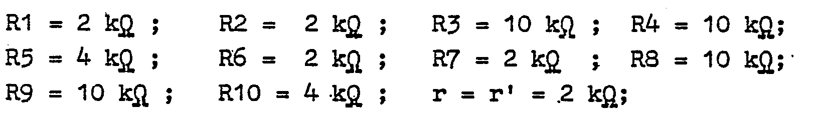
- Für den Kondensator C2 empfiehlt sich ein Kapazitätswert von beispielsweise C1 = (w.R10)-1 = 7 pF für 5,5 MHz.
- Anstelle der npn-Transistoren könnten auch pnp-Transistoren verwendet werden. Allerdings ist aus bekannten Gründen die beschriebene Ausführungsform mit npn-Transistoren besser.
- Wesentlich an der in Fig. 2 dargestellten Oszillatorschaltüng gemäß der Erfindung ist somit:
- 1.) Der Oszillator weist zwei Verstärkerstufen T2,T4 und T9,T10 auf, während die in Fig. 1 dargestellte Grundform der Erfindung nur eine solche Verstärkerstufe , nämlich T2, T4 aufweist. Dadurch ist bei der Oszillatorschaltung nach Fig. 2 eine Frequenzänderung durch Stromsteuerung an diesen beiden Stufen möglich.
- 2.) Die NF-Signaleinspeisung liegt nicht im HF-Signalweg, so daß keine Beeinflussung zwischen dem HF-Weg und dem NF-Weg auftritt.
- 3.) Das FM-modulierte HF-Signal kann rückwirkungsarm an den Anschlüssen 5, 6 (bzw. 9, 10) mit geringem Oberwellenanteil entnommen werden.
- 4.) Die Modulation ist nur mit einem sehr kleinen Modulationsklirrfäktor behaftet.
- Man erkennt ohne weiteres, daß sich die Schaltung gemäß Fig. 1 sowie die Schaltung gemäß Figur 2 (höchstens mit Ausnahme des Schwingkreises L1, C1) sich ohne Schwierigkeiten monolithisch integrieren läßt. Schließlich können auch die in der Schaltung verwendeten Transistoren durch Feldeffekttransistoren, insbesondere durch selbstsperrende MOS-Feldeffekttransistoren, z.B. vom n-Kanaltyp, ersetzt werden.
Claims (6)
Priority Applications (1)
| Application Number | Priority Date | Filing Date | Title |
|---|---|---|---|
| AT84109769T ATE47774T1 (de) | 1983-09-15 | 1984-08-16 | Integrierbare oszillatorschaltung. |
Applications Claiming Priority (2)
| Application Number | Priority Date | Filing Date | Title |
|---|---|---|---|
| DE3333402 | 1983-09-15 | ||
| DE19833333402 DE3333402A1 (de) | 1983-09-15 | 1983-09-15 | Integrierbare oszillatorschaltung |
Publications (3)
| Publication Number | Publication Date |
|---|---|
| EP0141933A2 true EP0141933A2 (de) | 1985-05-22 |
| EP0141933A3 EP0141933A3 (en) | 1986-08-13 |
| EP0141933B1 EP0141933B1 (de) | 1989-11-02 |
Family
ID=6209198
Family Applications (1)
| Application Number | Title | Priority Date | Filing Date |
|---|---|---|---|
| EP84109769A Expired EP0141933B1 (de) | 1983-09-15 | 1984-08-16 | Integrierbare Oszillatorschaltung |
Country Status (5)
| Country | Link |
|---|---|
| US (1) | US4565978A (de) |
| EP (1) | EP0141933B1 (de) |
| JP (1) | JPS6085605A (de) |
| AT (1) | ATE47774T1 (de) |
| DE (2) | DE3333402A1 (de) |
Cited By (2)
| Publication number | Priority date | Publication date | Assignee | Title |
|---|---|---|---|---|
| DE3938760A1 (de) * | 1989-11-23 | 1991-05-29 | Telefunken Electronic Gmbh | Abstimmbarer resonanzverstaerker oder oszillator |
| EP0509124A1 (de) * | 1991-04-19 | 1992-10-21 | Siemens Aktiengesellschaft | Oszillatorschaltung |
Families Citing this family (7)
| Publication number | Priority date | Publication date | Assignee | Title |
|---|---|---|---|---|
| GB2181914B (en) * | 1985-10-22 | 1989-09-20 | Plessey Co Plc | Frequency doubling oscillator and heterodyne circuit incorporating same |
| JPH01160103A (ja) * | 1987-12-16 | 1989-06-23 | Matsushita Electric Ind Co Ltd | 発振回路 |
| US5479137A (en) * | 1993-12-14 | 1995-12-26 | Samsung Electronics Co., Ltd. | Controlled oscillator, as for synchyronous video detector |
| DE4418432A1 (de) * | 1994-05-26 | 1995-11-30 | Siemens Ag | Frequenzveränderbare Oszillatoranordnung |
| DE60227885D1 (de) * | 2001-06-26 | 2008-09-11 | Nxp Bv | Schaltung zur Erzeugung einer negativen, relativ frequenzunabhängigen Konduktanz- |
| US7701303B2 (en) * | 2006-12-29 | 2010-04-20 | Infineon Technologies Ag | Oscillator with Darlington nodes |
| ITMI20090125A1 (it) * | 2009-02-03 | 2010-08-04 | Milano Politecnico | Oscillatore elettronico con ridotto rumore di fase |
Family Cites Families (6)
| Publication number | Priority date | Publication date | Assignee | Title |
|---|---|---|---|---|
| DE2059888B2 (de) * | 1970-12-05 | 1973-04-19 | Deutsche Itt Industries Gmbh, 7800 Freiburg | Monolithisch integrierbare oszillatorschaltung mit freuqenzbestimmendem zweipol |
| US3963996A (en) * | 1974-09-05 | 1976-06-15 | Zenith Radio Corporation | Oscillation system for integrated circuit |
| CH1384974A4 (de) * | 1974-10-16 | 1976-07-15 | ||
| JPS53111264A (en) * | 1977-03-10 | 1978-09-28 | Sony Corp | Oscillator |
| US4243953A (en) * | 1979-02-16 | 1981-01-06 | Rca Corporation | Voltage controlled oscillator presenting high impedance to parallel resonant tank circuit |
| JPS56147502A (en) * | 1980-04-18 | 1981-11-16 | Matsushita Electric Ind Co Ltd | Oscillator |
-
1983
- 1983-09-15 DE DE19833333402 patent/DE3333402A1/de not_active Withdrawn
-
1984
- 1984-08-16 EP EP84109769A patent/EP0141933B1/de not_active Expired
- 1984-08-16 DE DE8484109769T patent/DE3480371D1/de not_active Expired
- 1984-08-16 AT AT84109769T patent/ATE47774T1/de active
- 1984-08-30 US US06/646,005 patent/US4565978A/en not_active Expired - Fee Related
- 1984-09-12 JP JP59191431A patent/JPS6085605A/ja active Granted
Cited By (3)
| Publication number | Priority date | Publication date | Assignee | Title |
|---|---|---|---|---|
| DE3938760A1 (de) * | 1989-11-23 | 1991-05-29 | Telefunken Electronic Gmbh | Abstimmbarer resonanzverstaerker oder oszillator |
| EP0509124A1 (de) * | 1991-04-19 | 1992-10-21 | Siemens Aktiengesellschaft | Oszillatorschaltung |
| US5198784A (en) * | 1991-04-19 | 1993-03-30 | Siemens Aktiengesellschaft | Frequency modulated oscillator having controllable current sources |
Also Published As
| Publication number | Publication date |
|---|---|
| DE3480371D1 (en) | 1989-12-07 |
| DE3333402A1 (de) | 1985-04-04 |
| EP0141933A3 (en) | 1986-08-13 |
| EP0141933B1 (de) | 1989-11-02 |
| JPH0344685B2 (de) | 1991-07-08 |
| ATE47774T1 (de) | 1989-11-15 |
| JPS6085605A (ja) | 1985-05-15 |
| US4565978A (en) | 1986-01-21 |
Similar Documents
| Publication | Publication Date | Title |
|---|---|---|
| EP0051179B1 (de) | Integrierbare-Oszillatorschaltung | |
| DE3486100T2 (de) | Oszillatorschaltung. | |
| DE69623292T2 (de) | Bipolarer analogmultiplizierer für niederspannungsanwendungen | |
| DE69407902T2 (de) | Verstärkungsstufe und Oszillator | |
| DE3875713T2 (de) | Oszillatorschaltung und quadratur netzwerk fuer radioempfaenger. | |
| EP0141933B1 (de) | Integrierbare Oszillatorschaltung | |
| EP0073929A2 (de) | Integrierbare signalverarbeitende Halbleiterschaltung | |
| DE69226320T2 (de) | Negativen Widerstand verwendender spannungsgesteuerter Oszillator | |
| DE2622422A1 (de) | Butler-oszillator | |
| DE68924922T2 (de) | Oszillator. | |
| DE69010916T2 (de) | Differenzverstärker mit eingangsdämpfungsglied. | |
| DE2005888B2 (de) | Überlagerungsoszillator-Transistorschaltung | |
| DE3041392C2 (de) | Oszillatorschaltung mit einer Mischstufe | |
| EP0462304B1 (de) | Schaltungsanordnung zur Regelung der Amplituden eines Oszillators | |
| DE2438473A1 (de) | Transistorschaltung | |
| DE1261191B (de) | Mischschaltung | |
| AT394649B (de) | Anordnung zum abstimmen eines empfaengers auf einen gewaehlten kanal aus einer vielzahl von kanaelen | |
| EP0133618B1 (de) | Monolithisch integrierte Transistor-Hochfreqzenz-Quarzoszillatorschaltung | |
| DE2946952C2 (de) | ||
| DE3687446T2 (de) | Symmetrischer oszillator. | |
| DE1516789B2 (de) | Oszillatorschaltung | |
| EP0429896B1 (de) | Abstimmbarer Resonanzverstärker oder Oszillator | |
| DE3246295A1 (de) | Frequenzmodulierbarer oszillator | |
| DE2904045C2 (de) | Quarzoszillator mit gemischt induktiver und kapazitiver Schwingfrequenzsteuerung | |
| EP0370576A2 (de) | Oszillator |
Legal Events
| Date | Code | Title | Description |
|---|---|---|---|
| PUAI | Public reference made under article 153(3) epc to a published international application that has entered the european phase |
Free format text: ORIGINAL CODE: 0009012 |
|
| AK | Designated contracting states |
Designated state(s): AT DE FR GB IT NL |
|
| PUAL | Search report despatched |
Free format text: ORIGINAL CODE: 0009013 |
|
| AK | Designated contracting states |
Kind code of ref document: A3 Designated state(s): AT DE FR GB IT NL |
|
| 17P | Request for examination filed |
Effective date: 19860905 |
|
| 17Q | First examination report despatched |
Effective date: 19880616 |
|
| GRAA | (expected) grant |
Free format text: ORIGINAL CODE: 0009210 |
|
| AK | Designated contracting states |
Kind code of ref document: B1 Designated state(s): AT DE FR GB IT NL |
|
| REF | Corresponds to: |
Ref document number: 47774 Country of ref document: AT Date of ref document: 19891115 Kind code of ref document: T |
|
| REF | Corresponds to: |
Ref document number: 3480371 Country of ref document: DE Date of ref document: 19891207 |
|
| ET | Fr: translation filed | ||
| ITF | It: translation for a ep patent filed | ||
| GBT | Gb: translation of ep patent filed (gb section 77(6)(a)/1977) | ||
| PLBE | No opposition filed within time limit |
Free format text: ORIGINAL CODE: 0009261 |
|
| STAA | Information on the status of an ep patent application or granted ep patent |
Free format text: STATUS: NO OPPOSITION FILED WITHIN TIME LIMIT |
|
| 26N | No opposition filed | ||
| PGFP | Annual fee paid to national office [announced via postgrant information from national office to epo] |
Ref country code: AT Payment date: 19910726 Year of fee payment: 8 |
|
| ITTA | It: last paid annual fee | ||
| PGFP | Annual fee paid to national office [announced via postgrant information from national office to epo] |
Ref country code: NL Payment date: 19910831 Year of fee payment: 8 |
|
| PG25 | Lapsed in a contracting state [announced via postgrant information from national office to epo] |
Ref country code: AT Effective date: 19920816 |
|
| PG25 | Lapsed in a contracting state [announced via postgrant information from national office to epo] |
Ref country code: NL Effective date: 19930301 |
|
| NLV4 | Nl: lapsed or anulled due to non-payment of the annual fee | ||
| REG | Reference to a national code |
Ref country code: GB Ref legal event code: 711B |
|
| REG | Reference to a national code |
Ref country code: GB Ref legal event code: 711G |
|
| REG | Reference to a national code |
Ref country code: GB Ref legal event code: 732E |
|
| REG | Reference to a national code |
Ref country code: GB Ref legal event code: IF02 |
|
| PGFP | Annual fee paid to national office [announced via postgrant information from national office to epo] |
Ref country code: GB Payment date: 20030813 Year of fee payment: 20 |
|
| PGFP | Annual fee paid to national office [announced via postgrant information from national office to epo] |
Ref country code: FR Payment date: 20030820 Year of fee payment: 20 |
|
| PGFP | Annual fee paid to national office [announced via postgrant information from national office to epo] |
Ref country code: DE Payment date: 20030930 Year of fee payment: 20 |
|
| PG25 | Lapsed in a contracting state [announced via postgrant information from national office to epo] |
Ref country code: GB Free format text: LAPSE BECAUSE OF EXPIRATION OF PROTECTION Effective date: 20040815 |
|
| REG | Reference to a national code |
Ref country code: GB Ref legal event code: PE20 |