EP0141561A2 - Verfahren zur Herstellung von Bauelementen, die eine halbisolierende Zusammensetzung mit Indiumphosphid als Bestandteil haben - Google Patents
Verfahren zur Herstellung von Bauelementen, die eine halbisolierende Zusammensetzung mit Indiumphosphid als Bestandteil haben Download PDFInfo
- Publication number
- EP0141561A2 EP0141561A2 EP84307026A EP84307026A EP0141561A2 EP 0141561 A2 EP0141561 A2 EP 0141561A2 EP 84307026 A EP84307026 A EP 84307026A EP 84307026 A EP84307026 A EP 84307026A EP 0141561 A2 EP0141561 A2 EP 0141561A2
- Authority
- EP
- European Patent Office
- Prior art keywords
- iron
- indium
- semi
- indium phosphide
- ferrocene
- Prior art date
- Legal status (The legal status is an assumption and is not a legal conclusion. Google has not performed a legal analysis and makes no representation as to the accuracy of the status listed.)
- Granted
Links
Images
Classifications
-
- C—CHEMISTRY; METALLURGY
- C30—CRYSTAL GROWTH
- C30B—SINGLE-CRYSTAL GROWTH; UNIDIRECTIONAL SOLIDIFICATION OF EUTECTIC MATERIAL OR UNIDIRECTIONAL DEMIXING OF EUTECTOID MATERIAL; REFINING BY ZONE-MELTING OF MATERIAL; PRODUCTION OF A HOMOGENEOUS POLYCRYSTALLINE MATERIAL WITH DEFINED STRUCTURE; SINGLE CRYSTALS OR HOMOGENEOUS POLYCRYSTALLINE MATERIAL WITH DEFINED STRUCTURE; AFTER-TREATMENT OF SINGLE CRYSTALS OR A HOMOGENEOUS POLYCRYSTALLINE MATERIAL WITH DEFINED STRUCTURE; APPARATUS THEREFOR
- C30B25/00—Single-crystal growth by chemical reaction of reactive gases, e.g. chemical vapour-deposition growth
- C30B25/02—Epitaxial-layer growth
-
- C—CHEMISTRY; METALLURGY
- C30—CRYSTAL GROWTH
- C30B—SINGLE-CRYSTAL GROWTH; UNIDIRECTIONAL SOLIDIFICATION OF EUTECTIC MATERIAL OR UNIDIRECTIONAL DEMIXING OF EUTECTOID MATERIAL; REFINING BY ZONE-MELTING OF MATERIAL; PRODUCTION OF A HOMOGENEOUS POLYCRYSTALLINE MATERIAL WITH DEFINED STRUCTURE; SINGLE CRYSTALS OR HOMOGENEOUS POLYCRYSTALLINE MATERIAL WITH DEFINED STRUCTURE; AFTER-TREATMENT OF SINGLE CRYSTALS OR A HOMOGENEOUS POLYCRYSTALLINE MATERIAL WITH DEFINED STRUCTURE; APPARATUS THEREFOR
- C30B29/00—Single crystals or homogeneous polycrystalline material with defined structure characterised by the material or by their shape
- C30B29/10—Inorganic compounds or compositions
- C30B29/40—AIIIBV compounds wherein A is B, Al, Ga, In or Tl and B is N, P, As, Sb or Bi
Definitions
- This invention relates to a process for producing devices having semi-insulating indium phosphide based materials.
- III-V semiconductor materials such as gallium arsenide, indium phosphide, gallium indium phosphide, indium phosphide arsenide, and gallium indium arsenide phosphide are being utilized and/or have been investigated for various devices.
- these devices such as laser devices or Field Effect Transistors (FETs) are formed by a series of deposition processes resulting in a layered structure formed on an essentially single crystal substrate.
- FETs Field Effect Transistors
- a region is introduced within the structure to confine or restrict the flow of current to desired device paths, i.e., to device active regions.
- Various expedients such as a patterned oxide layer or a reverse biased p-n junction are employed for this isolation.
- the oxide layer does not permit epitaxial overgrowth.
- the p-n junction expedient which does allow overgrowth, nevertheless, yields a resistivity that is highly temperature dependent.
- Semi-insulating material is generally formed by suitably doping the desired III-V semiconductor material.
- one method of forming a semi-insulating gallium arsenide region involves introducing chromium as a dopant.
- the chromium doped gallium arsenide layer is generally fabricated by chemical vapor deposition (CVD) growth in a gas transport system.
- CVD chemical vapor deposition
- a gallium arsenide wafer is heated and a deposition gas is prepared that includes gallium chloride and arsenic compounds such as A S2 and/or As 4 . These materials are transported in a hydrogen stream or in an inert gas stream, e.g., a helium stream.
- gallium arsenide is deposited with the release of a chloride containing gas. The reactions involved are, thus, shown in the following equations. or
- An appropriate dopant precursor is introduced into the deposition gas stream to produce the desired semi-insulating properties.
- a chromyl chloride dopant precursor as described in U. S. Patent 4,204,893 issued May 27, 1980 is utilized for producing semi-insulating gallium arsenide.
- chromium compounds are not the only dopant precursors that have been suggested for doping gallium arsenide.
- Other dopant precursors such as iron pentacarbonyl for gallium arsenide doping have been disclosed. (See U. S. Patent 3,492,175 issued January 27, 1970.)
- Indium phosphide has also been formed by a C VD process.
- a gas stream including volatile indium halide entities such as InCl, InCl 2 , and In 2 CL 3 and phosphorus containing entities such as PH 3' P 2 and P 4 are utilized in a hydrogen atmosphere to form indium phosphide and HC1 as shown in the following equation.
- an inert gas carrier system such as a helium carrier system does not result in the deposition of indium phosphide. Since a reducing carrier e.g., a hydrogen carrier, is necessary in conventional CVD of indium phosphide, the dopant precursor employed has been limited to those that do not undergo reduction to produce elemental metals of low volatility.
- Indium phosphide having a resistivity up to 1 x 10 9 ohm-cm has been produced utilizing a metal organic chemical vapor deposition (MOCVD) procedure in conjunction with an iron pentacarbonyl or ferrocene based dopant precursor.
- MOCVD metal organic chemical vapor deposition
- the use of an iron pentacarbonyl or ferrocene based dopant precursor in the formation of indium phosphide through MOCVD results in device quality semi-insulating layers and avoids significant loss of dopant through premature deposition of elemental iron.
- the device active regions are produced by conventional techniques.
- inventions to be described involve the use of either a ferrocene or iron pentacarbonyl based dopant precursor (or a combination of such precursors) in conjunction with an indium-organic material to produce growth of a semi-insulating, i.e., resistivity of at least 10 3 ohm-cm, indium phosphide-based material and ultimately to produce a device.
- a semi-insulating, i.e., resistivity of at least 10 3 ohm-cm, indium phosphide-based material and ultimately to produce a device.
- the metal organic deposition of indium phosphide has been extensively described in articles such as "GaAs and Related Compounds," J.P. Duchemin, M. Bonnet, G.Beuchet, and F.
- indium alkyls such as trimethyl indium and triethyl indium where the alkyl preferably has 1 to 5 carbon atoms in conjunction with a source of phosphorus, e.g., phosphine, produce indium phosphide of satisfactory quality.
- a source of phosphorus e.g., phosphine
- alkyl indium materials are introduced separately into the gas deposition stream, there are several advantages in first forming an adduct between the indium-organic and an alkyl phosphine such as trimethyl phosphine and/or triethyl phosphine, where the alkyl of the phosphine preferably has 1 to 5 carbon atoms.
- Solid materials such as trimethyl indium are brought into the gas state through sublimation utilizing a gas stream such as a hydrogen gas stream.
- Liquid materials such as triethyl indium
- these materials generally have low vapor pressures, and thus adequate concentration is difficult to attain. Raising the bubbler temperature to avoid this difficulty results in disadvantageous decompositions, while increasing the carrier flow results in incomplete saturation of the gas.
- the adduct of the trialkyl indium compound and the trialkyl phosphine is a low melt point solid that is employable in a stable liquid form at moderately elevated temperatures and that is easily introduced into a gas stream by bubbling a gas such as hydrogen through it.
- the trialkyl indium compounds alone are vigorously pyrophoric while the adduct is not pyrophoric.
- the adduct is also useful, but not essential as an expedient, for preventing undesirable polymerization of the organo-indium compound.
- the adduct is introduced into the gas stream by flowing a gas, e.g., hydrogen or an inert gas such as nitrogen or helium, through a bubbler containing it.
- a gas e.g., hydrogen or an inert gas such as nitrogen or helium
- the gas be relatively pure so that impurities are not introduced into the deposited indium phosphide.
- Sufficient carrier gas e.g., hydrogen or an inert gas such as nitrogen or helium, is then flowed through the bubbler to produce a saturated combination of carrier gas and gas-based adduct. (The flow need not necessarily be saturated but much greater control is achieved by utilizing a saturated gas flow.
- gas flows in the range 50 to 200 sccm are utilized with a bubbler heated to a temperature in the range 60 to 100 degrees C to produce a saturated gas flow.
- a controlled sample is employed to determine suitable conditions for producing saturation for a given adduct.
- a source of phosphorus e.g., phosphine
- a source of phosphorus e.g., phosphine
- organic-indium compound of at least 50:1, preferably at least 75:1.
- Ratios less than 50:1 generally allow phosphorus escape from the already deposited indium phosphide layer. This escape yields a generally degraded morphology for the deposited indium phosphide.
- ratios greater than 100:1, although not precluded, are also not desirable since they are uneconomic.
- the dopant precursor a ferrocene and/or an iron pentacarbonyl based composition
- a mole ratio of iron to indium in the gas stream in the range 1 .2 x 10 -4 to 1 x 10⁻⁵.
- Molar ratios significantly higher than 1.2 x 10 -4 lead to inclusion of a second composition phase in the deposition while molar ratios less than 1 x 10 lead to insufficient resistivities in deposited indium phosphide-based layers having a background carrier concentration of approximately 2 x 10 15 cm 3 .
- Indium phosphide having a lower background concentration requires less dopant compensation. Thus, lower ratios for such materials are not precluded.
- iron pentacarbonyl based compositions A wide variety of iron pentacarbonyl based compositions is employable.
- an iron pentacarbonyl based composition such as butadiene iron tricarbonyl, cyclooctatetraene iron tricarbonyl, 1,3-pentadiene iron tricarbonyl, iron pentacarbonyl, cyclohexadiene iron tricarbonyl, cycloheptadiene iron tricarbonyl, cycloheptatriene iron tricarbonyl, cyclopentadienyl iron dicarbonyl dimer, and methylcyclopentadienyl iron dicarbonyl dimer are employable.
- ferrocenes is also employable.
- ferrocene dimethyl ferrocene, vinyl ferrocene, and butyl ferrocene are also useful.
- Conventional techniques are utilized to introduce the dopant precursor.
- a gas flow such as a hydrogen gas flow is passed over the ferrocene to induce sublimation.
- Typical gas flows in the range 5 to 20 sccm passed over the ferrocene at a temperature in the range 0 to 25 degrees C produce the desired ratio of indium to iron in the gas stream.
- an effusion source is preferably utilized.
- a gas flow such as a hydrogen gas flow
- a gas flow control means such as an electronic mass flow controller or needle valve that is adjusted to yield the desired iron-to-indium ratio and then passed over the effusion source containing the precursor, e.g., iron pentacarbonyl.
- the invention also extends to indium phosphide-based materials in general, i.e., indium phosphide as well as ternary and quarternary systems that include both indium and phosphorus such as indium gallium phosphide, indium phosphide arsenide, indium gallium aluminum phosphide, and indium gallium arsenide phosphide.
- either arsenic and/or gallium and/or aluminum is introduced into the gas stream by expedients such as, respectively, an admixture of AsH 3 and use of a bubbler containing alkyl gallium and/or alkyl aluminum compounds such as described in Journal of Crystal Growth, 55, 64 (1981), by J. P. Duchemin et al. Formation of device active regions and, indeed completion of the device such as an array of lasers and/or optoelectronic integrated circuit, are then accomplished by conventional techniques.
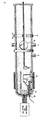
- a polished indium phosphide substrate, 5, measuring 1.91 x 2.54 cm (3/4 x 1 inch) and 0.0254 cm (0.010 inch) in thickness was cleaned in methanol and placed on a silicon carbide coated graphite susceptor, 10. This susceptor, together with the substrate, was positioned on the sample holder, 15, through loading port, 20, of a quartz reactor tube measuring 70 mm inside diameter. The susceptor was then moved to the growth position using rod, 25 and magnet, 35. A hydrogen flow was then established over the substrate at a rate of 5.5 1/min.
- a trimethyl indium/trimethyl phosphine adduct was prepared by mixing the two components in a mole ratio of 1 part trimethyl indium to 1.2 parts trimethyl phosphine. This adduct was purified by sublimation to yield a 1:1 adduct and then placed in a bubbler that was heated to a temperature of 70 degrees C. Approximately 25 grams of ferrocene were placed in a sublimer that was held at 10 degrees C. A 140 sccm flow of hydrogen was passed through the adduct bubler, and a 20 sccm H 2 flow was passed through the sublimer. Then the combined flow was directed through a line that bypassed the reactor. The susceptor was heated by subjecting it to an r.f.
- thermocouple, 30 sufficient to raise the substrate temperature to 700 degrees C as measured by thermocouple, 30.
- a flow of 1000 sccms of a 5 percent by volume mixture of PH 3 in H 2 was substituted for an equivalent flow of the original hydrogen flow through the reactor. (This initial flow was employed to prevent substrate decomposition.)
- the r.f. heating was continued until the substrate reached a temperature of 700 degrees C.
- the r.f. heating was then adjusted to maintain the substrate at this temperature.
- the combined hydrogen flows were transferred from the bypass line and combined with the PH 3/ H 2 flow. (These conditions produced an InP growth rate of approximately 2.5 pm per hour.)
- Example 1 The procedure of Example 1 was employed, except the dopant precursor was iron pentacarbonyl rather than ferrocene. This precursor was introduced utilizing an effusion source at -17 degrees C with a 20 sccm H 2 flow. The resulting layer had a resistivity of approximately 10 8 ohm-cm.
- a polished indium phosphide substrate measuring 1.91 x 2.54 cm (3/4 x 1 inch) and 0.0254 cm (0.010 inch) in thickness was cleaned in methanol and placed on a silicon carbide coated graphite susceptor, 10. This susceptor, together with the substrate, was positioned on the sample holder, 15, through loading port, 20 of a quartz reactor tube measuring 70 mm inside diameter. The susceptor was then moved to the growth position using rod, 25, and magnet, 35. A hydrogen flow was then established over the substrate at a rate of 6 1/min.
- a trimethyl indium/trimethyl phosphine adduct was prepared by mixing the two components in a mole ratio of 1 part trimethyl indium to 1.2 parts trimethyl phosphine. This adduct was purified by sublimation to yield a 1:1 adduct and then placed in a bubbler that was heated to a temperature of 70 degrees C. Approximately 10 grams of butadiene iron tricarbonyl were placed in a sublimer that was held at -6 degrees C. A 140 sccm flow of hydrogen was passed through the adduct bubbler, and a 5 sccm H 2 flow was passed through the sublimer. Then the combined flow was directed through a line that bypassed the reactor.
- the susceptor was heated by subjecting it to an r.f. power sufficient to raise the substrate temperature to 650 degrees C as measured by thermocouple 30.
- a flow of 750 sccm of a 5 percent by volume mixture of PH 3 in H 2 was substituted for an equivalent flow of the original hydrogen flow through the reactor. (This initial flow was employed to prevent substrate decomposition.)
- the r.f. heating was continued until the substrate reached a temperature of 650 degrees C.
- the r.f. heating was then adjusted to maintain the substrate at this temperature.
- the combined hydrogen flows were transferred from the bypass line and combined with the PH 3 /H 2 flow. (These conditions produced an InP growth rate of approximately 4 ⁇ m per hour.)
- Example 3 The procedure of Example 3 was followed except cyclooctatetraene iron tricarbonyl was employed rather than butadiene iron tricarbonyl. Additionally, the temperature of the cyclooctatetraene iron tricarbonyl sublimer was 9 degrees C, and the hydrogen flow through the sublimer was 20 sccm. The resistivity of the resulting doped indium phosphide was 6 x 10 7 ohm-cm.
Landscapes
- Chemical & Material Sciences (AREA)
- Engineering & Computer Science (AREA)
- Crystallography & Structural Chemistry (AREA)
- Materials Engineering (AREA)
- Metallurgy (AREA)
- Organic Chemistry (AREA)
- Chemical Kinetics & Catalysis (AREA)
- General Chemical & Material Sciences (AREA)
- Inorganic Chemistry (AREA)
- Chemical Vapour Deposition (AREA)
- Crystals, And After-Treatments Of Crystals (AREA)
Applications Claiming Priority (4)
| Application Number | Priority Date | Filing Date | Title |
|---|---|---|---|
| US54421583A | 1983-10-21 | 1983-10-21 | |
| US544215 | 1983-10-21 | ||
| US60437084A | 1984-04-26 | 1984-04-26 | |
| US604370 | 1984-04-26 |
Publications (3)
| Publication Number | Publication Date |
|---|---|
| EP0141561A2 true EP0141561A2 (de) | 1985-05-15 |
| EP0141561A3 EP0141561A3 (en) | 1986-04-02 |
| EP0141561B1 EP0141561B1 (de) | 1989-07-26 |
Family
ID=27067538
Family Applications (1)
| Application Number | Title | Priority Date | Filing Date |
|---|---|---|---|
| EP19840307026 Expired EP0141561B1 (de) | 1983-10-21 | 1984-10-15 | Verfahren zur Herstellung von Bauelementen, die eine halbisolierende Zusammensetzung mit Indiumphosphid als Bestandteil haben |
Country Status (4)
| Country | Link |
|---|---|
| EP (1) | EP0141561B1 (de) |
| JP (1) | JPS60149776A (de) |
| CA (1) | CA1210526A (de) |
| DE (1) | DE3479138D1 (de) |
Cited By (2)
| Publication number | Priority date | Publication date | Assignee | Title |
|---|---|---|---|---|
| EP0276069A3 (en) * | 1987-01-20 | 1989-02-15 | American Telephone And Telegraph Company | Vapor phase epitaxial growth of iron-doped, indium-based, compound group iii-v semiconductors |
| US5079184A (en) * | 1989-06-16 | 1992-01-07 | Kabushiki Kaisha Toshiba | Method of manufacturing iii-iv group compound semiconductor device |
Family Cites Families (7)
| Publication number | Priority date | Publication date | Assignee | Title |
|---|---|---|---|---|
| GB885514A (en) * | 1957-01-18 | 1961-12-28 | Union Carbide Corp | Acetylene transition metal carbonyl derivatives |
| US3164621A (en) * | 1963-04-12 | 1965-01-05 | Ethyl Corp | Cyclo-octadiene iron subgroup metal carbonyls |
| US3421952A (en) * | 1966-02-02 | 1969-01-14 | Texas Instruments Inc | Method of making high resistivity group iii-v compounds and alloys doped with iron from an iron-arsenide source |
| JPS5347765A (en) * | 1976-10-13 | 1978-04-28 | Matsushita Electric Ind Co Ltd | Semiconductor crystal growth method |
| US4314873A (en) * | 1977-07-05 | 1982-02-09 | The United States Of America As Represented By The Secretary Of The Navy | Method for depositing heteroepitaxially InP on GaAs semi-insulating substrates |
| GB1600286A (en) * | 1977-07-19 | 1981-10-14 | Secr Defence | Doping of group iii-v semiconductor materials |
| JPS5489566A (en) * | 1977-12-27 | 1979-07-16 | Fujitsu Ltd | Growth method of compound semiconductor crystal |
-
1984
- 1984-09-12 CA CA000463003A patent/CA1210526A/en not_active Expired
- 1984-10-15 EP EP19840307026 patent/EP0141561B1/de not_active Expired
- 1984-10-15 DE DE8484307026T patent/DE3479138D1/de not_active Expired
- 1984-10-20 JP JP59219405A patent/JPS60149776A/ja active Granted
Cited By (2)
| Publication number | Priority date | Publication date | Assignee | Title |
|---|---|---|---|---|
| EP0276069A3 (en) * | 1987-01-20 | 1989-02-15 | American Telephone And Telegraph Company | Vapor phase epitaxial growth of iron-doped, indium-based, compound group iii-v semiconductors |
| US5079184A (en) * | 1989-06-16 | 1992-01-07 | Kabushiki Kaisha Toshiba | Method of manufacturing iii-iv group compound semiconductor device |
Also Published As
| Publication number | Publication date |
|---|---|
| JPH0582734B2 (de) | 1993-11-22 |
| CA1210526A (en) | 1986-08-26 |
| EP0141561B1 (de) | 1989-07-26 |
| EP0141561A3 (en) | 1986-04-02 |
| JPS60149776A (ja) | 1985-08-07 |
| DE3479138D1 (en) | 1989-08-31 |
Similar Documents
| Publication | Publication Date | Title |
|---|---|---|
| US4716130A (en) | MOCVD of semi-insulating indium phosphide based compositions | |
| US4404265A (en) | Epitaxial composite and method of making | |
| US4147571A (en) | Method for vapor epitaxial deposition of III/V materials utilizing organometallic compounds and a halogen or halide in a hot wall system | |
| Moss et al. | A new approach to MOCVD of indium phosphide and gallium-indium arsenide | |
| US5124278A (en) | Amino replacements for arsine, antimony and phosphine | |
| US5244829A (en) | Organometallic vapor-phase epitaxy process using (CH3)3 As and CCl4 for improving stability of carbon-doped GaAs | |
| US3888705A (en) | Vapor phase growth of groups iii-v compounds by hydrogen chloride transport of the elements | |
| US4830982A (en) | Method of forming III-V semi-insulating films using organo-metallic titanium dopant precursors | |
| JPH0280572A (ja) | アルシン、アンチモン及びホスフィン置換体 | |
| EP0148357B1 (de) | Verfahren zum chemischen Abscheiden von siliziumdotierten intermetallischen Halbleiterverbindungen unter Verwendung metallorganischer Dämpfe | |
| US4488914A (en) | Process for the epitaxial deposition of III-V compounds utilizing a continuous in-situ hydrogen chloride etch | |
| JPH06252057A (ja) | 半導体装置の製造方法 | |
| US4782034A (en) | Semi-insulating group III-V based compositions doped using bis arene titanium sources | |
| US4279670A (en) | Semiconductor device manufacturing methods utilizing a predetermined flow of reactive substance over a dopant material | |
| US6211539B1 (en) | Semi-insulated indium phosphide based compositions | |
| EP0524817B1 (de) | Verfahren zur Kristallzüchtung eines III-V Verbindungshalbleiters | |
| EP0141561B1 (de) | Verfahren zur Herstellung von Bauelementen, die eine halbisolierende Zusammensetzung mit Indiumphosphid als Bestandteil haben | |
| JP3386302B2 (ja) | 化合物半導体へのn型ドーピング方法およびこれを用いた化学ビーム堆積方法並びにこれらの結晶成長方法によって形成された化合物半導体結晶およびこの化合物半導体結晶によって構成された電子デバイスおよび光デバイス | |
| EP0293439B1 (de) | Halbisolierende, auf iii-v-elementen basierende materialien | |
| US5622559A (en) | Method of preparing compound semiconductor | |
| Chen et al. | The use of triisopropylantimony for the growth of InSb and GaSb | |
| JPH0654764B2 (ja) | 半絶縁性ガリウムヒ素形成方法 | |
| CA1287555C (en) | Metalorganic vapor phase epitaxial growth of group ii-vi semiconductor materials | |
| KR900006121B1 (ko) | 도우펀트 운반 화합물로서 테트라메틸주석을 사용하는 반도체 재료층의 에피택셜 증착방법 | |
| JP3141628B2 (ja) | 化合物半導体素子及びその製造方法 |
Legal Events
| Date | Code | Title | Description |
|---|---|---|---|
| PUAI | Public reference made under article 153(3) epc to a published international application that has entered the european phase |
Free format text: ORIGINAL CODE: 0009012 |
|
| AK | Designated contracting states |
Designated state(s): DE FR GB NL |
|
| PUAL | Search report despatched |
Free format text: ORIGINAL CODE: 0009013 |
|
| AK | Designated contracting states |
Kind code of ref document: A3 Designated state(s): DE FR GB NL |
|
| 17P | Request for examination filed |
Effective date: 19860904 |
|
| 17Q | First examination report despatched |
Effective date: 19880209 |
|
| GRAA | (expected) grant |
Free format text: ORIGINAL CODE: 0009210 |
|
| AK | Designated contracting states |
Kind code of ref document: B1 Designated state(s): DE FR GB NL |
|
| REF | Corresponds to: |
Ref document number: 3479138 Country of ref document: DE Date of ref document: 19890831 |
|
| ET | Fr: translation filed | ||
| PLBE | No opposition filed within time limit |
Free format text: ORIGINAL CODE: 0009261 |
|
| STAA | Information on the status of an ep patent application or granted ep patent |
Free format text: STATUS: NO OPPOSITION FILED WITHIN TIME LIMIT |
|
| 26N | No opposition filed | ||
| REG | Reference to a national code |
Ref country code: GB Ref legal event code: IF02 |
|
| PGFP | Annual fee paid to national office [announced via postgrant information from national office to epo] |
Ref country code: FR Payment date: 20020923 Year of fee payment: 19 |
|
| PGFP | Annual fee paid to national office [announced via postgrant information from national office to epo] |
Ref country code: GB Payment date: 20020926 Year of fee payment: 19 |
|
| PGFP | Annual fee paid to national office [announced via postgrant information from national office to epo] |
Ref country code: NL Payment date: 20021003 Year of fee payment: 19 |
|
| PGFP | Annual fee paid to national office [announced via postgrant information from national office to epo] |
Ref country code: DE Payment date: 20021205 Year of fee payment: 19 |
|
| PG25 | Lapsed in a contracting state [announced via postgrant information from national office to epo] |
Ref country code: GB Free format text: LAPSE BECAUSE OF NON-PAYMENT OF DUE FEES Effective date: 20031015 |
|
| PG25 | Lapsed in a contracting state [announced via postgrant information from national office to epo] |
Ref country code: NL Free format text: LAPSE BECAUSE OF NON-PAYMENT OF DUE FEES Effective date: 20040501 Ref country code: DE Free format text: LAPSE BECAUSE OF NON-PAYMENT OF DUE FEES Effective date: 20040501 |
|
| GBPC | Gb: european patent ceased through non-payment of renewal fee |
Effective date: 20031015 |
|
| PG25 | Lapsed in a contracting state [announced via postgrant information from national office to epo] |
Ref country code: FR Free format text: LAPSE BECAUSE OF NON-PAYMENT OF DUE FEES Effective date: 20040630 |
|
| NLV4 | Nl: lapsed or anulled due to non-payment of the annual fee |
Effective date: 20040501 |
|
| REG | Reference to a national code |
Ref country code: FR Ref legal event code: ST |