EP0137148A2 - Elektrostatische Sonde - Google Patents
Elektrostatische Sonde Download PDFInfo
- Publication number
- EP0137148A2 EP0137148A2 EP84108330A EP84108330A EP0137148A2 EP 0137148 A2 EP0137148 A2 EP 0137148A2 EP 84108330 A EP84108330 A EP 84108330A EP 84108330 A EP84108330 A EP 84108330A EP 0137148 A2 EP0137148 A2 EP 0137148A2
- Authority
- EP
- European Patent Office
- Prior art keywords
- drive
- oscillator
- shield
- sense
- layer
- Prior art date
- Legal status (The legal status is an assumption and is not a legal conclusion. Google has not performed a legal analysis and makes no representation as to the accuracy of the status listed.)
- Granted
Links
Images


Classifications
-
- G—PHYSICS
- G03—PHOTOGRAPHY; CINEMATOGRAPHY; ANALOGOUS TECHNIQUES USING WAVES OTHER THAN OPTICAL WAVES; ELECTROGRAPHY; HOLOGRAPHY
- G03G—ELECTROGRAPHY; ELECTROPHOTOGRAPHY; MAGNETOGRAPHY
- G03G15/00—Apparatus for electrographic processes using a charge pattern
- G03G15/50—Machine control of apparatus for electrographic processes using a charge pattern, e.g. regulating differents parts of the machine, multimode copiers, microprocessor control
- G03G15/5033—Machine control of apparatus for electrographic processes using a charge pattern, e.g. regulating differents parts of the machine, multimode copiers, microprocessor control by measuring the photoconductor characteristics, e.g. temperature, or the characteristics of an image on the photoconductor
- G03G15/5037—Machine control of apparatus for electrographic processes using a charge pattern, e.g. regulating differents parts of the machine, multimode copiers, microprocessor control by measuring the photoconductor characteristics, e.g. temperature, or the characteristics of an image on the photoconductor the characteristics being an electrical parameter, e.g. voltage
-
- G—PHYSICS
- G01—MEASURING; TESTING
- G01R—MEASURING ELECTRIC VARIABLES; MEASURING MAGNETIC VARIABLES
- G01R29/00—Arrangements for measuring or indicating electric quantities not covered by groups G01R19/00 - G01R27/00
- G01R29/12—Measuring electrostatic fields or voltage-potential
-
- G—PHYSICS
- G01—MEASURING; TESTING
- G01R—MEASURING ELECTRIC VARIABLES; MEASURING MAGNETIC VARIABLES
- G01R29/00—Arrangements for measuring or indicating electric quantities not covered by groups G01R19/00 - G01R27/00
- G01R29/24—Arrangements for measuring quantities of charge
Definitions
- This invention relates to a probe and its associated circuit for measuring the voltage level of an electrostatically charged surface and more particularly to the unique construction of a vibrating piezoceramic probe and its unique circuit.
- the probe can be applied to any process or machine for the measurement of electrostatic surface potential, including electrophotographic copier and print machines.
- a photoconductive material receives a relatively uniform charge level which may be, for example, 800 volts. Since the photoconductive material is an insulator, that charge remains on the material until it is exposed to light. When exposed, the exposed portion of the photoconductor is discharged to a level which can approach zero volts. In the electrophotographic process, the exposed photoconductor is then developed and a print is made from the developed image.
- a relatively uniform charge level which may be, for example, 800 volts. Since the photoconductive material is an insulator, that charge remains on the material until it is exposed to light. When exposed, the exposed portion of the photoconductor is discharged to a level which can approach zero volts. In the electrophotographic process, the exposed photoconductor is then developed and a print is made from the developed image.
- Print quality in an electrophotographic machine deteriorates over a period of time as the electrostatic properties of the photoconductive material change with age.
- repeated use of the photoconductor can change surface properties and effect print quality. For example, repeated application of developing material can film the surface and make it less receptive to light.
- the surface of the photoconductor is roughened and darkened.
- electrostatic probes are placed near the photoconductive surface to sense changes in electrostatic charge level.
- either the developer bias level can be adjusted in order to compensate for the changes. See, for example, the system described in U.S. Patent No. 4,326,796.
- probes When probes are used to measure the charge on an electrostatic surface, an initial requirement is to establish a reference to calibrate the significance of the measured quantity.
- the charge level of the drum seal can provide the needed reference since such a seal is grounded or at some other known potential.
- chopping schemes are often used to momentarily shield the probe from the unknown voltage on the photoconductive surface and replace it with a reference voltage.
- the probe of this invention utilizes a different scheme, a nulling arrangement where the photoconductor voltage is successively compared to a known voltage which is _varied until the two are equal.
- Schemes of this type utilize a vibrating sense electrode placed between a surface of unknown potential (the photoconductor) and another surface of known potential. As the electrode vibrates, the 15 between the unknown potential and the sense electrode changes to generate a current in the electrode. That current is used to increase or decrease the potential on the known surface until it equals the photoconductor voltage. At that point, the vibrating electrode output is reduced to zero.
- Vibrating probes generally have three elements, a drive element, a sense element, and a feedback element.
- Tuning forks are usually used as the vibrator and have a magnetic or piezoelectric element attached as a driver to set the tuning fork into oscillation.
- a sense element, a conductor of some kind, is attached to the tuning fork, and a feedback element is often attached in order to maintain the frequency of the tuning fork at resonance.
- Such probes are difficult to manufacture and are expensive.
- the object of this invention is to eliminate bulky apparatus such as tuning forks to enable close positioning of the vibrating probe to the surface to be measured in order to improve probe sensitivity and reduce its cost.
- this invention provides a probe for measuring electrostatic potential where the probe is made from a single piezoceramic bender element surrounded (except for a sense window) by a shield at a known potential.
- the bender element is comprised of a piezoceramic drive layer connected to a drive oscillator, a sensing conductor, and a piezoceramic feedback layer also connected to the drive oscillator. As the oscillator supplies current to the piezoceramic drive element, the bender element deforms. Deformation of the bender element includes a deformation of the piezoceramic feedback element thus inducing a current in the feedback layer.
- the induced current is fed back to the oscillator to tune the output of the oscillator to the natural resonant frequency of the bender element.
- the sense element (part of the vibrating bender element) is placed near the electrostatic potential to be measured, and is located within the field generated between the shield and the surface to be measured. As the crystal bender element vibrates, a current is induced in the conducting sense element due to the change of capacitance as the sense element moves toward and away from the photoconductor.
- the current thus produced is connected to an amplifying, filtering and phase sensing circuit so that adjustments can be made to the known potential on the shield in order to eliminate the presence of the electrostatic field. When that occurs, there is no further induced current in the sense element and the known potential on the shield is equal to the surface potential to be measured.
- this invention provides a small, simple and cheap electrostatic probe comprised of a single bender element which acts as a drive element, a sensor element and a feedback element all in one.
- the simple probe of this invention To operate properly, it is necessary to float the sensed voltage (in the millivolt range) on the known potential provided on the probe shield (which may be several hundred volts). Additionally, the sensed voltage (which is many times larger) and the oscillator drive voltage must itself float on the known potential on the shield. Finally, the oscillator drive voltage must be disconnected from the oscillator during the measurement period in order to decouple any low impedances in the oscillator voltage supply from the sense resistor. A unique circuit and ' shielding arrangement to implement this device is described herein.
- FIG. 1 is a diagrammatical representation showing the major components of a typical electrophotographic machine.
- a photoconductor 100 is mounted on the outer surface of a drum 101 which is driven to rotate in direction A. As the photoconductor passes under charge corona 102, a relatively uniform electrostatic charge is placed across the surface of the photoconductor.
- An image is produced by selectively discharging the photoconductor at the exposure station 103. The image is developed by developer 104 and is transferred to receiving material, usually paper, under the influence of transfer corona 105.
- a cleaning corona 106 precedes the cleaning station 107. The receiving material is moved along a paper path 108 in direction B.
- a probe unit 109 is located to sense the electrostatic voltage level present on the photoconductor. By locating the probe 109 subsequent to the exposure station 103, it is possible to sense the fully exposed voltage level of the photoconductor as well as the unexposed voltage level. These sensed voltage levels are fed to control circuits to adjust the charge corona 102, the intensity of illumination at exposure station 103, or the developer bias voltage level at developer 104.
- FIG. 2 is a block diagram of a measurement system for use with the electrostatic probe 109.
- a crystal bender element 10 is placed in close proximity to a photoconductive surface 100.
- the element 10 is surrounded by a shield 12 which is connected by line 49 to a known output potential supplied from the high voltage supply 13.
- Crystal bender element 10 is driven from a drive oscillator circuit 14 and current produced in the sense portion of bender element 10 is supplied across resistor 15 for detection by the sense amplifier 16.
- the output of amplifier 16 is then filtered and compared to the phase of the drive oscillator in circuit 17 for altering the level of voltage supplied to shield 12 by high voltage supply circuit 13.
- the known voltage potential on shield 12 is adjusted until the crystal bender element 10 vibrates in an electrostatic field reduced to approximately zero potential. At that point, the current produced in the sense portion of bender element 10 is effectively reduced to zero and the known voltage from supply circuit 13 is equal to the unknown voltage to be measured.
- FIG. 2 Other elements of the circuit shown in FIG. 2 include a low voltage supply circuit 18 for driving the oscillator 14 and a connection 18a to the machine control logic 19 in order to enable the measurement of the photoconductor voltage at the proper time in the sequential operation of the host machine.
- Line 13a provides for high voltage shutdown and line 13b is the output line informing the machine control of the measurement value of the photoconductor voltage.
- Line 13b can carry analog or digital signals as required.
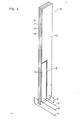
- FIG. 3 is a perspective view of the crystal bender element 10 showing the multilayered construction of that device.
- Layers 20 and 22 are made of piezoceramic material (insulative material) and sandwich a conductive layer 24 therebetween.
- Layers 20 and 22 are covered with thin conductive coats 20a and 22a along the outer surfaces thereof.
- the thin conductive surface 22a has been removed along area 28 to provide a separate conductive area 26.
- conductive surface 22a When in use, conductive surface 22a is positioned nearest to the surface to be sensed and is the capacitive sensing element into which a current is induced by vibratory motion. Conductive surface 22a is connected by line 23 to layer 24 by line 25 to shield 12 (connected to layer 32 or shield 12 as fully shown in FIG. 6, to be described later). Shield 12 is connected to the sense resistor and amplifier.
- Piezoceramic layer 20 is the drive element and is connected through line 21 to the output of the oscillator circuit 14 and by layer 24 and line 25 to the shield 12 to complete the circuit to the oscillator common (as shown more fully in FIG. 6, described later).
- Conductive area 26 acts as a part of the feedback element (together with piezoceramic layer 22) and is connected by line 27 to the input of the oscillator and through layer 24, line 25 and the shield 12 to the oscillator common (FIG. 6).
- Piezoceramic bender elements of the type shown in FIG. 3 are commercially available and are typically used as plate resonators for the transmission and reception of acoustic signals. They are commonly used for remote control devices to change channels in a television set.
- the commercially available bender element is altered to provide the construction shown in FIG. 3 by etching the surface 22a at area 28 to provide the feedback element 26 separate from the sense element 22a.
- FIG. 4 shows a cutaway side view of the electrostatic probe assembly with the crystal bender element 10 shown mounted in relation to the shield 12. Any appropriate mounting means can be used including an epoxy compound 8 with an appropriate spacer 9.
- FIG. 4 shows that the shield 12 is a multilayered shield made up of three materials, an outer conducting element 30, an insulating element 31 and an inner conducting element 32. An air gap 33 is maintained between shield 12 and bender element 10, and the bender element 10 is positioned near the photoconductive surface 100.
- FIG. 5 is a front view of the probe looking toward it from the photoconductive surface.
- FIG. 5 shows that the conductive surface 22a is exposed to the photoconductive surface through an opening (window) in the shield 12.
- FIG. 6 shows the details of a suitable drive oscillator circuit for use with the probe of this invention.
- the circuit shown in FIG. 6 is the same as that shown in FIG. 2 except that a second shield 45' has been provided around the drive oscillator and a voltage follower circuit 7 has been provided to feed the sensed current into the sense amplifier 16.
- the purpose of the second shield 45' is to provide a low impedance shield around the drive oscillator to limit the amount of stray voltage signals which might be picked up and provided to the sense amplifier. In that manner, the number of filter stages can be reduced.
- FIG. 6 shows that an operational amplifier 40 provides an output drive signal over line 21 to the drive element 20.
- Positive feedback is provided from feedback element 26 through line 27 to amplifier 40.
- Resistors R1 and R2 together with capacitance C3 are used to set the phase relationship of the feedback signal in order to provide a closed loop gain greater than one. With this circuit, positive feedback occurs and the circuit breaks into oscillation at the resonant frequency of the piezoceramic bender element.
- the drive oscillator is connected to a low voltage supply (12 volts) supplied through field effect transistors (FETs) 41, 42 and 43.
- FET 43 acts to float the oscillator common at the high voltage supply output signal to allow circuit operation with a high voltage reference.
- the high voltage signal is also connected through line 44 to the inner shield 45.
- a machine control 19 acts to open the switches 41, 42, and 43 during a measurement period thus allowing the circuit to additionally float on the sensed potential.
- machine control 19 closes the switches at a suitable time prior to the measurement period in order to set the bender element into oscillation and to charge energy storing elements, capacitors Cl and C2. Those capacitors are used to continue driving the oscillator during the measurement period when the low voltage source is disconnected.
- An optical isolator comprised of light source 46 and photodetector 47 is used to isolate the shield 45 from low impedance feedback which might be present in the phase detector circuit 17a. It also acts to isolate the high voltage common used in the drive oscillator from ground used in the phase detector 17a.
- a second optical isolator 48 is similarly used to isolate the high voltage 48 is similarly used to isolate the high voltage common in the sense amplifying and filter circuit from the ground used with the phase detector.
- Sense load resistor 15 is connected between line 49 which is at high voltage potential and line 50 which is also at high voltage potential but which carries the current produced in sense element 22a as well.
- the current flow in sensing resistor 15 is produced by only the few millivolts of potential difference between lines 49 and 50 due to the sense element 22a. In that manner, the sensed voltage of a few millivolts rides on the high voltage signal of perhaps 800 volts and, despite that, can be detected to provide an appropriate drive for the sense amplifier 16.
- the sense signal Since the drive oscillator operates at a 12 volt potential and the sense signal is only a few millivolts, the sense signal must be shielded from the oscillator drive signal. It is primarily for that reason that the oscillator circuit is encased in shield 45. Note that shield 45 is at high voltage potential and thus the oscillator voltage of 12 volts also floats on the high voltage signal.
- sense resistor 15 is a high impedance element. To prevent the coupling of any low impedances in parallel with resistor 15, the low voltage supply circuit is disconnected by switch 43 during the measurement period. Also, the optical isolator formed by light source 46 and photodetector 47 is used to decouple low impedances in the phase detector.
- the sensing element 22a is positioned close to the photoconductor field produced between the photoconductor and the high voltage potential present on shield 32 (which is connected to shield 45).
- the capacitances of the element 22a with respect to the photoconductor 100 changes.
- the change in the charge Q produced on the sense element 22a creates a current flow and it is that current flow that is coupled through line 25, shield plate 32, and shield 45 to the sense resistor 15.
- the electrostatic field potential V is effectively eliminated and the current produced in the vibrating sense element 22a is effectively reduced to zero.
- the voltage on line 49 is a measure of the voltage on the photoconductor 100.
- element 22 is a piezoceramic device
- a second voltage is induced into the sense element 22a as a result of the physical stress placed upon element 22 as it is deformed by drive element 20.
- This piezoceramic induced voltage is not coupled back into resistor 15 since connector 23, FIG.3, places both sides of the element 22 (conductors 22a and 24) at the same potential.
- current in element 22a produced by the piezoelectric effect in element 22 are shorted back across the crystal 22.
- FIG. 5 note that the feedback element 26 is located outside the influence of the electrostatic field between photoconductor 11 and shield 32. As a consequence, the feedback voltages produced in the element 26 are the result of the piezoelectric effect and not the result of vibration in the electrostatic field.
- FIGS. 3 and 6 show that element 26 is connected through line 27 to one side of the drive oscillator and the other side of the drive oscillator (oscillator common) through conducting layer 24 and line 25 to shields 32 and 45. In that manner, a circuit is provided through the piezoceramic element 26 so that the piezoelectric feedback voltage produced therein is fed back to the oscillator.
- the electrostatic probe and its associated circuit has been discussed with reference to an electrophotographic machine in sensing the voltage on a photoconductor, the probe and its circuit are of value in any application in which accurate sensing of an electrostatic field is needed. For example, in many processes relating to the production of various plastic articles it may be desirable to sense for a buildup of charge on the surface of the plastic. This probe and its unique construction would be of value in such an application.
Landscapes
- Physics & Mathematics (AREA)
- General Physics & Mathematics (AREA)
- Engineering & Computer Science (AREA)
- Microelectronics & Electronic Packaging (AREA)
- Control Or Security For Electrophotography (AREA)
Applications Claiming Priority (2)
| Application Number | Priority Date | Filing Date | Title |
|---|---|---|---|
| US531565 | 1983-09-13 | ||
| US06/531,565 US4625176A (en) | 1983-09-13 | 1983-09-13 | Electrostatic probe |
Publications (3)
| Publication Number | Publication Date |
|---|---|
| EP0137148A2 true EP0137148A2 (de) | 1985-04-17 |
| EP0137148A3 EP0137148A3 (en) | 1986-06-04 |
| EP0137148B1 EP0137148B1 (de) | 1988-11-30 |
Family
ID=24118160
Family Applications (1)
| Application Number | Title | Priority Date | Filing Date |
|---|---|---|---|
| EP84108330A Expired EP0137148B1 (de) | 1983-09-13 | 1984-07-16 | Elektrostatische Sonde |
Country Status (4)
| Country | Link |
|---|---|
| US (1) | US4625176A (de) |
| EP (1) | EP0137148B1 (de) |
| JP (1) | JPS6067866A (de) |
| DE (1) | DE3475441D1 (de) |
Cited By (4)
| Publication number | Priority date | Publication date | Assignee | Title |
|---|---|---|---|---|
| WO1994002965A1 (en) * | 1992-07-17 | 1994-02-03 | Cookson Group Plc | Ceramic deflection device |
| GB2272976A (en) * | 1992-11-30 | 1994-06-01 | Stewart Hughes Ltd | Electrostatic charge sensor |
| EP0682263A3 (de) * | 1994-05-09 | 1996-02-28 | Xerox Corp | Eine abgeschirmte Elektrode und Kohlefaserleiter verwendendes elektrostatisches Voltmeter mit Waagebalken-Modulator. |
| WO2021191520A1 (fr) * | 2020-03-26 | 2021-09-30 | Office National D'etudes Et De Recherches Aérospatiales | Detecteur de champ electrique |
Families Citing this family (22)
| Publication number | Priority date | Publication date | Assignee | Title |
|---|---|---|---|---|
| US4763078A (en) * | 1986-03-27 | 1988-08-09 | Williams Bruce T | Sensor for electrostatic voltmeter |
| US4928057A (en) * | 1986-10-28 | 1990-05-22 | Williams Bruce T | High speed D.C. non-contacting electrostatic voltage follower |
| JPH01170862A (ja) * | 1987-12-05 | 1989-07-05 | Bruce T Williams | 静電電圧計用センサ |
| US4879577A (en) * | 1988-04-19 | 1989-11-07 | International Business Machines Corporation | Method and apparatus for controlling the electrostatic parameters of an electrophotographic reproduction device |
| US5241276A (en) * | 1989-04-28 | 1993-08-31 | Kabushiki Kaisha Toshiba | Surface potential measuring system |
| US5070302A (en) * | 1989-09-05 | 1991-12-03 | Eastman Kodak Company | Capacitance probe for measuring a width of a clearance between parts |
| US5164673A (en) * | 1989-11-13 | 1992-11-17 | Rosener Kirk W | Induced electric field sensor |
| US5212451A (en) * | 1992-03-09 | 1993-05-18 | Xerox Corporation | Single balanced beam electrostatic voltmeter modulator |
| JPH0823568B2 (ja) * | 1993-04-14 | 1996-03-06 | 日本電気株式会社 | 電位センサ |
| WO1994029733A1 (de) * | 1993-06-16 | 1994-12-22 | Franz Winkler | Verfahren zur kontaktlosen bestimmung elektrischer messgrössen |
| JPH0716899U (ja) * | 1993-08-31 | 1995-03-20 | リズム時計工業株式会社 | 疑似扉構造 |
| US5617020A (en) * | 1995-06-07 | 1997-04-01 | Regents Of The University Of California | Microelectromechanical-based power meter |
| US5594331A (en) * | 1995-06-07 | 1997-01-14 | Regents Of The University Of California | Microelectromechanical powerline monitoring apparatus |
| US6300756B2 (en) * | 1996-06-12 | 2001-10-09 | The Trustees Of Princeton University | Micro-mechanical probes for charge sensing |
| US5943223A (en) * | 1997-10-15 | 1999-08-24 | Reliance Electric Industrial Company | Electric switches for reducing on-state power loss |
| JP2002039709A (ja) * | 2000-07-28 | 2002-02-06 | Mitsutoyo Corp | 静電容量式プローブデバイス及び変位測定回路 |
| US8222886B2 (en) | 2008-06-18 | 2012-07-17 | Hioki Denki Kabushiki Kaisha | Voltage detecting apparatus and line voltage detecting apparatus having a detection electrode disposed facing a detected object |
| JP2010256125A (ja) * | 2009-04-23 | 2010-11-11 | Hioki Ee Corp | 電圧検出装置および線間電圧検出装置 |
| US7890005B2 (en) * | 2009-01-07 | 2011-02-15 | Infoprint Solutions Company, Llc | Adjusting electrostatic charges used in a laser printer |
| US9638549B2 (en) * | 2014-10-31 | 2017-05-02 | Ememory Technology Inc. | Integrated capacitance sensing module and associated system |
| TWI601962B (zh) | 2016-12-21 | 2017-10-11 | 財團法人工業技術研究院 | 靜電檢測系統與方法 |
| CN111132437B (zh) * | 2019-12-11 | 2023-06-06 | 维沃移动通信有限公司 | 一种移动终端 |
Family Cites Families (17)
| Publication number | Priority date | Publication date | Assignee | Title |
|---|---|---|---|---|
| US3379972A (en) * | 1963-12-26 | 1968-04-23 | Reliance Electric & Eng Co | Non-contacting displacement gauge having a feedback means for controlling the vibration amplitude of the probe |
| US3739299A (en) * | 1972-04-20 | 1973-06-12 | Zenith Radio Corp | Adjustable piezoelectric tunable oscillator for acoustic signal generating system |
| US3788739A (en) * | 1972-06-21 | 1974-01-29 | Xerox Corp | Image compensation method and apparatus for electrophotographic devices |
| FR2252575B1 (de) * | 1973-11-23 | 1979-03-16 | Lewiner Jacques | |
| GB1542837A (en) * | 1974-10-28 | 1979-03-28 | Avo Ltd | Voltage measuring apparatus |
| US4106869A (en) * | 1976-11-26 | 1978-08-15 | Xerox Corporation | Distance compensated electrostatic voltmeter |
| US4147981A (en) * | 1977-02-18 | 1979-04-03 | Williams Bruce T | Electrostatic voltmeter probe positioned on the outside of a housing and vibrated by a piezoelectric transducer within the housing |
| US4205267A (en) * | 1977-11-03 | 1980-05-27 | Williams Bruce T | High speed electrostatic voltmeter |
| US4267511A (en) * | 1977-11-09 | 1981-05-12 | Canon Kabushiki Kaisha | Surface potentiometer |
| JPS5467475A (en) * | 1977-11-09 | 1979-05-30 | Canon Inc | Surface potentiometer |
| US4266870A (en) * | 1978-03-09 | 1981-05-12 | Ricoh Company, Ltd. | Electrostatographic apparatus comprising developing bias means |
| US4189673A (en) * | 1978-05-01 | 1980-02-19 | Burroughs Corporation | Pen-shaped precision multi-level current mode logic test probe |
| US4367948A (en) * | 1979-04-24 | 1983-01-11 | Canon Kabushiki Kaisha | Surface potential electrometer and image forming apparatus using the same |
| US4326796A (en) * | 1979-12-13 | 1982-04-27 | International Business Machines Corporation | Apparatus and method for measuring and maintaining copy quality in an electrophotographic copier |
| US4370616A (en) * | 1980-08-15 | 1983-01-25 | Williams Bruce T | Low impedance electrostatic detector |
| US4473857A (en) * | 1982-06-10 | 1984-09-25 | Sencore, Inc. | Input protection circuit for electronic instrument |
| US4458172A (en) * | 1982-08-06 | 1984-07-03 | Hitachi, Ltd. | Ultrasonic probe |
-
1983
- 1983-09-13 US US06/531,565 patent/US4625176A/en not_active Expired - Fee Related
-
1984
- 1984-07-16 DE DE8484108330T patent/DE3475441D1/de not_active Expired
- 1984-07-16 EP EP84108330A patent/EP0137148B1/de not_active Expired
- 1984-08-10 JP JP59166675A patent/JPS6067866A/ja active Granted
Cited By (10)
| Publication number | Priority date | Publication date | Assignee | Title |
|---|---|---|---|---|
| WO1994002965A1 (en) * | 1992-07-17 | 1994-02-03 | Cookson Group Plc | Ceramic deflection device |
| GB2284298A (en) * | 1992-07-17 | 1995-05-31 | Cookson Group Plc | Ceramic deflection device |
| GB2284298B (en) * | 1992-07-17 | 1996-05-15 | Cookson Group Plc | Ceramic deflection device |
| GB2272976A (en) * | 1992-11-30 | 1994-06-01 | Stewart Hughes Ltd | Electrostatic charge sensor |
| GB2272976B (en) * | 1992-11-30 | 1996-06-05 | Stewart Hughes Ltd | A sensor |
| US5705930A (en) * | 1992-11-30 | 1998-01-06 | Stewart Hughes Limited | Gas path electrostatic sensor |
| EP0682263A3 (de) * | 1994-05-09 | 1996-02-28 | Xerox Corp | Eine abgeschirmte Elektrode und Kohlefaserleiter verwendendes elektrostatisches Voltmeter mit Waagebalken-Modulator. |
| WO2021191520A1 (fr) * | 2020-03-26 | 2021-09-30 | Office National D'etudes Et De Recherches Aérospatiales | Detecteur de champ electrique |
| FR3108728A1 (fr) * | 2020-03-26 | 2021-10-01 | Office National D'etudes Et De Recherches Aérospatiales | Detecteur de champ electrique |
| US11757408B2 (en) | 2020-03-26 | 2023-09-12 | Office National D'etudes Et De Recherches Aérospatiales | Electric field detector |
Also Published As
| Publication number | Publication date |
|---|---|
| EP0137148B1 (de) | 1988-11-30 |
| US4625176A (en) | 1986-11-25 |
| JPS642898B2 (de) | 1989-01-19 |
| JPS6067866A (ja) | 1985-04-18 |
| DE3475441D1 (en) | 1989-01-05 |
| EP0137148A3 (en) | 1986-06-04 |
Similar Documents
| Publication | Publication Date | Title |
|---|---|---|
| EP0137148B1 (de) | Elektrostatische Sonde | |
| US4314242A (en) | Apparatus for detecting a residual quantity of toner | |
| US3852667A (en) | Probe for electrostatic voltmeter | |
| US5006897A (en) | Determination of charge-to-mass ratio | |
| US3379972A (en) | Non-contacting displacement gauge having a feedback means for controlling the vibration amplitude of the probe | |
| US4918376A (en) | A.C. capacitive gauging system | |
| US4878017A (en) | High speed D.C. non-contacting electrostatic voltage follower | |
| US4147981A (en) | Electrostatic voltmeter probe positioned on the outside of a housing and vibrated by a piezoelectric transducer within the housing | |
| US4928057A (en) | High speed D.C. non-contacting electrostatic voltage follower | |
| US4553099A (en) | Electrostatic voltage sensor | |
| US6806717B2 (en) | Spacing compensating electrostatic voltmeter | |
| US5489850A (en) | Balanced beam electrostatic voltmeter modulator employing a shielded electrode and carbon fiber conductors | |
| US4868907A (en) | Self-biased scorotron grid power supply and electrostatic voltmeter operable therefrom | |
| US7548066B2 (en) | Potential measuring device and image forming apparatus using the same | |
| US4818945A (en) | Non contacting volt meter | |
| EP0666509B1 (de) | Erkennungsvorrichtung für Aufnahmematerial | |
| US4470009A (en) | Surface potentiometer | |
| US5077566A (en) | Image forming apparatus | |
| EP0168951A1 (de) | Elektrostatische Sonde für elektrophotographische Vorrichtung | |
| JPH08178986A (ja) | 電位センサ | |
| JPH07306081A (ja) | 粉体検知装置 | |
| US5532802A (en) | Piezoelectric sensor for in-situ monitoring of electrostatographic developers | |
| JPS5915864A (ja) | 表面電位検出装置 | |
| JPS6331058Y2 (de) | ||
| JPH09138254A (ja) | 電位センサ用検出回路 |
Legal Events
| Date | Code | Title | Description |
|---|---|---|---|
| PUAI | Public reference made under article 153(3) epc to a published international application that has entered the european phase |
Free format text: ORIGINAL CODE: 0009012 |
|
| 17P | Request for examination filed |
Effective date: 19841123 |
|
| AK | Designated contracting states |
Designated state(s): DE FR GB |
|
| 17P | Request for examination filed |
Effective date: 19850216 |
|
| XX | Miscellaneous (additional remarks) |
Free format text: DIE MELDUNG VOM 850502 BEZOG SICH AUF 137910 |
|
| PUAL | Search report despatched |
Free format text: ORIGINAL CODE: 0009013 |
|
| AK | Designated contracting states |
Kind code of ref document: A3 Designated state(s): DE FR GB |
|
| 17Q | First examination report despatched |
Effective date: 19880222 |
|
| GRAA | (expected) grant |
Free format text: ORIGINAL CODE: 0009210 |
|
| AK | Designated contracting states |
Kind code of ref document: B1 Designated state(s): DE FR GB |
|
| REF | Corresponds to: |
Ref document number: 3475441 Country of ref document: DE Date of ref document: 19890105 |
|
| ET | Fr: translation filed | ||
| PLBE | No opposition filed within time limit |
Free format text: ORIGINAL CODE: 0009261 |
|
| STAA | Information on the status of an ep patent application or granted ep patent |
Free format text: STATUS: NO OPPOSITION FILED WITHIN TIME LIMIT |
|
| 26N | No opposition filed | ||
| PGFP | Annual fee paid to national office [announced via postgrant information from national office to epo] |
Ref country code: FR Payment date: 19910625 Year of fee payment: 8 |
|
| PGFP | Annual fee paid to national office [announced via postgrant information from national office to epo] |
Ref country code: DE Payment date: 19910723 Year of fee payment: 8 |
|
| PGFP | Annual fee paid to national office [announced via postgrant information from national office to epo] |
Ref country code: GB Payment date: 19920624 Year of fee payment: 9 |
|
| PG25 | Lapsed in a contracting state [announced via postgrant information from national office to epo] |
Ref country code: FR Effective date: 19930331 |
|
| PG25 | Lapsed in a contracting state [announced via postgrant information from national office to epo] |
Ref country code: DE Effective date: 19930401 |
|
| REG | Reference to a national code |
Ref country code: FR Ref legal event code: ST |
|
| PG25 | Lapsed in a contracting state [announced via postgrant information from national office to epo] |
Ref country code: GB Effective date: 19930716 |
|
| GBPC | Gb: european patent ceased through non-payment of renewal fee |
Effective date: 19930716 |