EP0132833A2 - Digitaler Phasenumtastungsmodulator für ein Modulator-Demodulator-System - Google Patents
Digitaler Phasenumtastungsmodulator für ein Modulator-Demodulator-System Download PDFInfo
- Publication number
- EP0132833A2 EP0132833A2 EP84108741A EP84108741A EP0132833A2 EP 0132833 A2 EP0132833 A2 EP 0132833A2 EP 84108741 A EP84108741 A EP 84108741A EP 84108741 A EP84108741 A EP 84108741A EP 0132833 A2 EP0132833 A2 EP 0132833A2
- Authority
- EP
- European Patent Office
- Prior art keywords
- phase
- predetermined
- vector
- shift
- plane
- Prior art date
- Legal status (The legal status is an assumption and is not a legal conclusion. Google has not performed a legal analysis and makes no representation as to the accuracy of the status listed.)
- Withdrawn
Links
- 239000013598 vector Substances 0.000 claims abstract description 116
- 230000010363 phase shift Effects 0.000 claims abstract description 56
- 230000000694 effects Effects 0.000 claims description 2
- 230000004044 response Effects 0.000 claims description 2
- 125000004122 cyclic group Chemical group 0.000 abstract 1
- 230000005540 biological transmission Effects 0.000 description 13
- 230000008859 change Effects 0.000 description 13
- 230000006870 function Effects 0.000 description 12
- 238000012360 testing method Methods 0.000 description 11
- 239000003990 capacitor Substances 0.000 description 4
- 238000010586 diagram Methods 0.000 description 3
- 230000003595 spectral effect Effects 0.000 description 3
- 238000001228 spectrum Methods 0.000 description 3
- 230000007704 transition Effects 0.000 description 3
- 238000001914 filtration Methods 0.000 description 2
- 230000006872 improvement Effects 0.000 description 2
- 238000013459 approach Methods 0.000 description 1
- 238000006243 chemical reaction Methods 0.000 description 1
- 230000001427 coherent effect Effects 0.000 description 1
- 239000013078 crystal Substances 0.000 description 1
- 238000013461 design Methods 0.000 description 1
- 230000009191 jumping Effects 0.000 description 1
- 238000000034 method Methods 0.000 description 1
- 238000012545 processing Methods 0.000 description 1
- 230000009467 reduction Effects 0.000 description 1
- 239000004065 semiconductor Substances 0.000 description 1
- 238000012546 transfer Methods 0.000 description 1
Images
Classifications
-
- H—ELECTRICITY
- H04—ELECTRIC COMMUNICATION TECHNIQUE
- H04L—TRANSMISSION OF DIGITAL INFORMATION, e.g. TELEGRAPHIC COMMUNICATION
- H04L27/00—Modulated-carrier systems
- H04L27/18—Phase-modulated carrier systems, i.e. using phase-shift keying
-
- H—ELECTRICITY
- H04—ELECTRIC COMMUNICATION TECHNIQUE
- H04L—TRANSMISSION OF DIGITAL INFORMATION, e.g. TELEGRAPHIC COMMUNICATION
- H04L27/00—Modulated-carrier systems
- H04L27/18—Phase-modulated carrier systems, i.e. using phase-shift keying
- H04L27/20—Modulator circuits; Transmitter circuits
- H04L27/2032—Modulator circuits; Transmitter circuits for discrete phase modulation, e.g. in which the phase of the carrier is modulated in a nominally instantaneous manner
- H04L27/2092—Modulator circuits; Transmitter circuits for discrete phase modulation, e.g. in which the phase of the carrier is modulated in a nominally instantaneous manner with digital generation of the modulated carrier (does not include the modulation of a digitally generated carrier)
Definitions
- the present invention relates to transmission of information by phase shift keyed modulation, and particularly discloses an improved device for phase shift keyed (PSK) modulated data transmission wherein the signal transmitted by each keying of the transmitter is determined by a vector in a phase plane having one of a set of possible phases, wherein all allowable vectors have the same length.
- PSK phase shift keyed
- phase encoding information by the relative phase of a signal transmitted over the telephone line have been developed to increase the rate at which data may be transmitted over a band limited channel of a specified bandwidth.
- phase encoding has been differential four-phase, phase shift keyed (PSK) encoding.
- PSK phase shift keyed
- a carrier of a constant frequency is transmitted and information is encoded by differences in the relative phase of the carrier which occur at predetermined "bit times".
- the phase distortion of the transmission channel is ultimate an upper limit.
- differential four-phase PSK a carrier signal of a specified frequency (usually either 1200 or 2400 Hz) is transmitted.
- Each keying of the transmitter (each "bit time") will cause the transmitted signal to be characterized by one of four possible phases relative to its previous phase. Since there are four possible changes for .each keying of the transmitter, two bits may be encoded in each keying of the transmitter, and thus the scheme will transmit two bits per baud.
- a further specification of this popular form of data transmission is that the transmitter operated as 600 baud rate and thus 1200 bits per second may be transmitted.
- Microprocessors have been used in the past, to implement a number of different functions within a modem including demodulation of data. See for example U.S. Patent 4,431,867 to Dale A. Heatherington ' which is assigned to the assignee of the present invention.
- receivers The design of receivers is based on the premise that it is the relative phase between a present bit time and the previous bit time that is important to the receiver, and not the particular path by which. a vector in a phase plane representing the relative phase of the carrier signal took to arrive at its new phase value.
- the d ⁇ /dt characteristic of the transmission signal becomes more important. For example, for transmission at commonly used 600 baud/1200 bit per second four-phase PSK, a succession of 90° phase shifts will cause the phase lock loop in receiver to detect a shift in the _carrier frequency in excess of 100 Hz making tracking difficult.
- the present invention provides such an improved digital modulator.
- the present invention may be generally characterized as a digital PSK modulator wherein the resultant vector in a phase plane defining the relative phases of the carrier at different bit times (and thus the vector which defines the nature of the signal transmitted to the telephone line) is one which traces a straight line between all allowable phase points in the phase plane. This is an improvement on the more familiar arcuate path between allowable points in the phase plane which results from the phase shifting of a vector of constant length.
- the present invention includes means for generating a first signal at the carrier frequency and having a predetermined magnitude and a second signal at the carrier frequency also having a predetermined magnitude.
- the modulator is responsive to incoming data signals to encode N (N being an integer greater than zero) data bits to cause the signal from the first generator to initially change phase in a first sense with respect to a reference phase in the phase plane, and the signal of the other generator to initially change phase in a second and opposite sense from the reference phase.
- N being an integer greater than zero
- the modulator appropriately changes the phase of each of the signals from the two generators.
- the vector sum of the two is added to produce each output so that the locus of,points, in the phase plane, of the resultant vector defines a straight line between the reference phase, and the next phase representing encoded information.
- the invention directly synthesizes a modulated carrier signal which has a spectral characteristic substantially identical to prior art signals generated by shifting a single vector of constant length in the phase plane, after substantial filtering has been done to the prior art signal.
- the present invention directly provides an output signal which requires lower order output filters, thus reducing the number of parts required to construct a modulator with acceptable out-of-band spectral components.
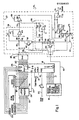
- Fig. 1 is a schematic diagram of the preferred embodiment.
- the preferred embodiment is included in a modem constructed around microprocessor 15.
- the type Z-8 microprocessor currently manufactured by Zilog Inc. of Cupertino, California is used.
- Microprocessor 15 is the eight megahertz version of the Z-8 processor and is driven by a 7.9872 megahertz crystal 16, as shown in Fig. 1.
- the Z-8 interfaces with other devices through four eight bit ports designated by the manufacturer as ports 0 through 3. This notation is used in Fig. 1.
- a portion of port 0 (lines P04--P07) and a portion of port 3 forms a seven line bus 17 _connected to a block 18 indicated as containing the modem receiver, the RS-232 interface, status indicators, and other circuits.
- a modem in which the preferred embodiment resides, will also be controlled by microprocessor 15.
- the preferred embodiment described below has been constructed so that at least 30% of the processor time is available to control the other functions represented by block 18. Exemplary details of how - other functions of a modem may be controlled through the Z-8 processor may be found in the .present inventor's co-pending application serial No. 273,398, filed June 15, 1981 entitled "Modem With Low Part Count and Improved Demodulator". Said application serial No. 273,398 is hereby incorporated by reference exactly as if set forth herein.
- the line attached to pin 30 designated as 19 in Fig. 1 receives a signal from the RS-232 interface on line 20 designated TXD. This signal is inverted by inverting buffer 21 before being supplied to pin P30.
- the processor performs a serial to parallel conversion of the inverted data coming in on line 19 to form dibit pairs which are to be modulated by the preferred embodiment.
- the output signals of the present invention are generated by a sine table which resides in read only memory 22.
- Read only memory 22 is a four kilobyte read only memory with each byte being eight bits wide.
- the instructions which implement the steps shown in Fig. 4, together with the sine table described hereinbelow, reside within ROM 22.
- the processor will successively look up values from the sine table contained in ROM 22 and write appropriate values out to port 2, which is connected to a bus shown as 32 in Fig. 1.
- Bus 32 is connected to digital to analog converter 35 which provides an analog output on line 36 corresponding to the instantaneous value of the voltage to be transmitted.
- Line 36 is connected to the input to transmit filter 37.
- Transmit filter 37 is constructed of two two-pole band pass filters 38 and 39. These filters are constructed around a pair of operational amplifiers 40 and 41 which, in the preferred embodiment, are portions of a type LM338 currently manufactured by National Semiconductor, and others.
- filter 38 the frequency determining elements include capacitors 45 and 46 and resistors 47--50.
- filter 39 is constructed with capacitors 55 and 56 and resistors -57--61 determining the frequency response.
- a latched output from block 18 appears on line 62 to control operation of transistors 65, 66 and 67.
- Line 62 is held high or low according to whether the modem is in the originate or answer mode, which determines the frequency output from the preferred embodiment.
- transistors 65 and 66 are turned on, resistors 49 and 59 are shorted, changing the center frequency of filters 38 and 39.
- the outputs from filters 38 and 39 are algebraicly mixed by a circuit constructed around operational amplifier 68 which serves as a unity gain buffer by the choice of resistors 69 and 70 having equal values.
- the output from amplifier 68 appears on line 71 as an inputdto an all pass delay filter constructed around operational amplifiers 72 and 73.
- capacitors 75 and 76 and resistors 77--80 are the frequency determining elements for the all pass two-pole delay filter of the final stage of transmit filter 37.
- the all pass delay section of transmit filter 37 is designed to compensate for _ group delay distortion from filters 38 and 39.
- Capacitor 81 is a relatively large value to keep the points connected to line 82 high when transistors 65--67 are cut off.
- filter section 38 has a bandwidth of approximately 445 hertz with a center frequency of 800 hertz when the modem is operating in the originate mode, and a center frequency of 2800 hertz when in the answer mode.
- Filter section 39 has a bandwidth of approximately 265 hertz with a center frequency of 1650 hertz for originate and 2 kilohertz for the answer mode. From this description, it will be apparent that the characteristics of the band pass filters overlap in a manner to give a desirable pass band for the transfer function between line 36 and line 71 for a 600 baud Bell 212A-type modem.
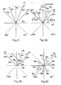
- Fig. 2 a representation of a phase plane for a carrier output signal is shown. It should be understood that the graph of the phase plane shows a vector 85 in various positions, shown as 85a, 85b...85e.
- the phase plane shown on Fig. 2 represents the phase of the vector, and thus the phase of a carrier signal relative to an arbitrary but predetermined reference shown on the positive X axis at 86.
- bit time is used in quotation marks above to indicate that it is actually a dibit being transmitted. but the common phraseology of referring to the center of a bit time as the center point between keyings of the transmitter will be used in this specification.
- Fig. 2 there are four allowable reference phases used in conventional four-phase differential PSK modulation. They are represented on Fig. 2 as line at 45, 135, 225, and 315' from the arbitrary reference phase shown by axis 86. These are considered four predetermined valid phases within the phase plane.
- the preferred embodiment is a differential four-phase PSK modulator
- the present invention is usable in other PSK modulators including coherent PSK, and N phase PSK encoding where N is an integer.
- PSK is a form of phase modulation, it follows that the spectrum of the output signal contains energy at frequencies other than the carrier.
- the necessary bandwidth to transmit differential PSK is a function of the baud rate.
- phase shifts of the type shown in Fig. 2 produce a considerable amount of energy outside the desired transmission bandwidth for differential PSK.
- Fig. 3A shows an exemplary 90' shift according to the present invention.
- the path that the vector representing the carrier signal, with reference to reference phase 86, tracks between the 45 and 135° phase points, is represented by dashed line 88.
- the angle 0 is shown relative to reference 86.
- Vector 90 begins at the 45° phase as shown at 90a in Fig. 3A.
- the present invention being a digital modulator
- the various locations of the vector 90 as represented in Fig. 3A will occur in discrete steps.
- the discrete steps are equal in time, but not equal in change of the angle ⁇ .
- path 88 is a straight line
- an improvement to the output signal is achieved by having the projection of vector 90 onto the X axis (for the example of a shift from 45 to 135 as shown) move as a cosine function of time.
- vectors 90a, 90b...90d change so that the projection along the X axis is a cosine function of time.
- the plus 90° phase shift takes place over N discrete steps, each of which is referred to by an index n.
- a sine table resides in ROM 22.
- the sine table is used to generate the output frequency according to the following formula:
- N is equal to an address in the sine table from which the next value is to be fetched
- F is equal to a frequency determining number which will be described below
- X is equal to the previous value of N and serves as a pointer to the sine table
- P equals a relative phase shift from the previous output of the carrier.
- the notation MOD(K) indicates that the modulo K result of the sum (F+X+P) is to be taken, and thus it can be considered the integer remainder after dividing by K.
- the sine table simply contains K entries giving the mine for each increment of angle which is 1/Kth of a full 360' (2 ⁇ tadians) circle.
- a look up to the sine table must be made at regularly spaced intervals which, in the preferred embodiment, is determined by internally generated interrupts at a predetermined interrupt frequency.
- K is equal to 128 and thus there are 128 entries in the sine table. This being the case, each time the address N advances by one, the argument of the value contained in the sine table advances 360'/128, or 2.813°, Selections of other values of K will lead to appropriately larger or smaller increments in the argument of the sine value contained in the table.
- N will be continuously incremented by 1 and one complete stepping through the entire sine table will take place at a rate determined by the interrupt frequency.
- a'fetch is made to the Nth location of the sine table contained in ROM 22 (Fig. 1), and the value of the sine table contained at that location could be written onto bus 32 and provided as an input to D to A converter 35. The analog output corresponding to this value in the sine table would appear on line 36.
- the sine table has been adequately described in words above, exemplary ones of the 12$ entries for the sine table are shown in the following table 2.
- the sine values are coded as non-signed integers taking values between 0 and 31, with 16 being the equivalent of 0 for a signed representation of the sine function.
- the integer value (as a decimal number) actually used in the sine table of the preferred embodiment is shown in the fourth column.
- a table driven sine wave generator as described above may be easily implemented to generate a phase shift keyed output signal as shown in Fig. 2.
- the desired result is to have the output vector trace a straight line 88 as shown in Fig. 3A, and for the projection of the output vector onto the X axis to trace a cosine function of time.
- n-2, 3 and 6 are shown on Fig. 3A. Since the angle 0 for vectors 90 shown on Fig. 3A should shift according to equation 4 and table 3 above, the only remaining problem is the fact that vector 90 becomes shorter as one proceeds from the 45 phase point towards the Y axis, and again become longer as one proceeds away from the Y axis toward the 135° phase point. Since the sine table described above in connection table 2 provides output values for a vector of unit length, it would at first appear that multiplication of the values output from the sine table in ROM 22 by processor 15 is required prior to outputinq the result to digital analog converter 35. Indeed, an embodiment of the present invention could be so constructed.
- arithmetic multiplication steps by processors such as Z-8 take a great deal more time that addition and subtraction steps.
- the processor is generating interrupts at 9600 hertz. Even though only half of these are used, the arrangement still requires that one complete step, for example, from vector 90b to 90c, be accomplished during one interrupt period of 104.2 microseconds. Since multiplication operations by the Z-8 take on the order of 50 microseconds, there is not sufficient time within the interrupt period to look up a value in the sine table and perform a muliplication in order to shorten a vector 90 so that the Y component will remain constant, as shown in Fig. 3A.
- vectors 95 and 96 are colinear and define the vector point in the phase plane.
- Each of vectors 95 and 96 is generated by a sine table driven generator as described hereinabove.
- vector 95 shifts in the opposite sense of the ultimate +90° shift that the resultant is to take.
- An exemplary first step is shown by vector 90a wherein it can be seen that vector 95a was provided a negative shift from the 45° angle and vector 96a was provided with a positive shift.
- a subsequent pair of vectors is _shown as 95b and 96b. From this point, vector 95b has begun moving with a positive phase shift while vector 96b has a positive phase shift.
- the resultant of these vectors is tracing straight line 88 to provide the desired results of the present invention.
- vectors 95c and 96c are provided with a negative phase shift as vector 95 continues to be provided with a positive phase shift until the vectors again become colinear, at the new predetermined phase in the phase plane, as shown at 95d and 96d.
- Each of the vectors 95 and 96 is generated by the same sine table described hereinabove contained in read only memory 22.
- vector 95 is considered vector 1 and vector 96 is considered vector 2
- a set of variables described as PMN can easily be generated where M refers to the vector number and N refers to the index n as shown in table 3.
- the inclusion of the apparatus of the processor and the sine table to generate each of vectors 95 and 96 may be considered the provision of a first generator for generating a first signal, vector 95, of a predetermined magnitude and a predetermined frequency at a first phase in a phase plane represented in Fig. 3B.
- the apparatus may be considered a second generator for generating a second signal, vector 96, of the same predetermined magnitude at the same predetermined frequency in the phase plane.
- the accumulator of the Z-8 processor is a mixing means for combining the first and second signals to provide a resultant signal which is characterized by a resultant vector having a resultant phase in the phase plane. This may be easily seen by the fact that the resultant of each of the pairs for vectors 95 and 96 shown on Fig. 3B lie at a predetermined point along line 88 and thus are characterized by a predetermined value of 0 as shown in table 3.
- phase shift control means which is responsive to the particular dibit, each dibit being one of a set of N (N being equal to 2) data signals which initially shifts the phase of vector 95 in a predetermined sense with respect to the _reference phase 86, and initially shifts vector 96 in the opposite sense with respect to the predetermined reference phase. Furthermore, the apparatus further responds to continue shifting the first and second phases of vectors 95 and 96 in discrete increments so that the locus of in points of the resultant vector defines a linear path in the phase plane between a first predetermined phase at the 45' point, and a second predetermined phase at the 135° point.
- Fig. 3C an exemplary 180° phase shift is shown.
- the present invention is one in which the path between the set of predetermined phase points is a straight line.
- the examplary 180° phase shift is shown between the 45° and the 225° points. Since it is also desired, for the 180° shift, that the projection of the resultant vectors along the line connecting the two points trace a cosine function of time, it will be readily appreciated that rotation of vectors 95 and 96 at a conrtant angular rate for the 180° case will accomplish this without resorting to the mathematics of equation 4 above.
- vectors 95 and 96 are merely rotated in opposite senses at a constant angular rate. This produces a resultant vector which retreats from the 45° point toward the origin and back out toward the 225° phase point in a manner which is a cosine function of time.
- vectors 95a and 96a are superimposed leading to a resultant shown at point 110 in the phase plane.
- the _ resultant of these vectors is indicated at point 111 in the phase plane.
- shifting continues until the point 95d and 96d is reached with the resultant being shown at 115, which is of equal magnitude to the resultant at 111.
- the final step of the 180' phase shift has the vectors again being colinear at an angle of 225° and the end point has been reached within the constraits of the present invention as described above.
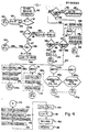
- the first step is represented at step 120 where the routine is entered from the internally generated 9600 hertz interrupt from the Z-8 processor.
- First step 121 is executed to determine if a parity flag F1 is set. If the answer is no, the interrupt which cause the program to enter step 120 is considered an even numbered interrupt and no branch 122 is taken to step 125. This occurs after _ flag F1 has been complemented at step 123.
- Step 125 leads to the output subroutine which begins at step 145 and eventually comes to return instruction 155.
- the output subroutine is described in detail hereinbelow. At this point, it should be understood that every other one of the 9600 Hz interrupts (for which F1 is equal to 0) will cause the program to execute the output subroutine providing a normal, non-phase shifted, progression through the sine table.
- step 121 On the next interrupt entered at step 120, step 121 will test positive, and a test to see if a counter variable CT1 has reached 8 is performed at step 126. Assuming for the moment this is negative, no branch 127 is taken to decisional step 128 to test test if flag FO has been set. Flag FO is set whenever the dibit pair 01, corresponding to no phase shift from the previous value, is detected. Thus, if the dibit currently being processed is one which requires a 0° phase shift, yes branch 129 is taken to jump step 130 noted as "go to A". If some other phase shift is in progress, no branch 131 will be taken to jump step 132 which provides a relative address contained in a pointer variable called PNTR.
- PNTR pointer variable
- the 0, 180, and +90° phase shifts will be described. From the +90° phase shifts, the steps for implementing -90° phase shifts will be apparent.
- the steps for implementing -90° phase shifts will be apparent.
- the first example assume that the previous phase shift has been accomplished and the yes branch 135 is taken from step 126. First the counter variable is cleared at 136 and the FO flag is cleared at step 137. Next, a sequence of tests of the value of the dibit about to be encoded begins with step 138.
- Subroutine A is entered at step 145.
- Subroutine A is the output routine which causes the generation of both vectors 95 and 96, as shown in Figs. 3B and 3C, and causes the resultant vector to be output to digital analog converter 35, and thus to continue transmission of the carrier signal.
- the variable RO is loaded with the value from the sine table determined by (F+Xl+PVl) MOD(K).
- Xl is the previous value of the pointer to the sine table (the address in the sine table) for the first vector. Since the phase variable PV1 for the first vector has not changed, the pointer to the sine table is simply incremented by an amount which corresponds to the constant frequency output, and thus no phase shift in the resultant output signal will be provided.
- the value of Xl is updated for the next pass through subroutine A.
- the value from the sine table for the second- vector is added to the previous value already contained in register R0.
- the value of X2, the sine table pointer for the second vector is updated for the next pass.
- Step 152 is an output step in which the eight bit value of variable RO is output from port 2 of processor 15, along bus 32, as the input to digital to analog converter 35.
- the resulting analog signal on line 36 is filtered by filter 37 and transmitted on output line 74 to the telephone line.
- step 121 the next interrupt which passes the parity test of step 121 will cause the following steps to be executed. Since the counter has not yet arrived at 8, branch 127 will be taken from step 126 and the FO flag will be tested at step 128.
- branch 135 will be taken from step 136.
- branch 158 will'be taken from step 138 to test 159. Since the present example assumes this test is positive, branch 160 will be taken to a subroutine enclosed with dashed line 165a.
- the first step of this subroutine is to add to variable PV1 a constant designated as Pll. As shown in table 4, Pll is the number to be algebraicly added to the phase variable P for vector 1 on the first step of a 90° phase shift.
- variable PV2 is incremented by a predetermined amount P21 at step 167. It should be noted, by reference to Fig. 3B, that Pll will be a negative number (vector 95 is considered vector 1) and constant P21 will be a positive number.
- the pointer variable PNTR is loaded with a constant referred to as NEXT1 at step 168. From here, a jump to subroutine A is made at step 170a.
- the test at step 126 fails as does the step at test 128. Since this occurs, no branch 131 is taken and the relative jump instruction at 132 jumps to an address determined by the pointing variable PNTR. Since, at step 168 within subroutine 165a, this was loaded with a value of NEXT1, the program jumps to entry point 171.
- Subroutine 165b is conceptually identical to subroutine 165a except that the constant values for -P12, P22, and NEXT2, are different. Thus, within subroutine 165b, the appropriate change in the phase variable for each of the vectors is made and, at step 170b, the output subroutine A is executed. The next time through the program, the value NEXT2 is the value of the pointer to which the program jumps at step 132 and thus entry point 179 for subroutine 165c is reached.
- the preferred embodiment of the present invention has been constructed so that the constant values, PMN, for change of phase of each .of the two vectors are stored in distinct subroutines together with a pointer to the next subroutine for the next incremental step across the 90° phase change. It has been found by the inventor of the present invention that the use of additional space in ROM 22 to store the separate subroutines wherein the variables for PMN are each written, together with the pointer to the next subroutine, is preferable to placing them in a look up table. Thus, a trade off has been made in favor of speed of execution at the cost of use of instruction ROM space.
- step 126 proceeds through subroutines 165c on to subroutine 165g to accomplish the phase changes shown in Fig. 3B. Once this has been accomplished, the next execution of step 126 will cause yes branch 135 to be taken indicating that this phase shift has been accomplished.
- step 185 the next step executed is to load the pointer PNTR with a constant value PNTX at step 186. This will cause the program to enter a subroutine 187 for constantly incrementing and decrementing the phase variables for the two vectors by the same amount on each subsequent pass through the program.
- the first step is step 188 in which the phase variable for the first variable is incremented by eight.
- the phase variable for the second variable is decremented by eight at step 189, and the program branches to the output routine at jump step 190.
- each of the vectors is stepped 22.5° for each of the eight steps through the 180° phase change. Since each incrementing of the address in the sine table corresponds to a stepping of 2.813°, changing the phase variable by eight corresponds to a phase shift of 22.5° and thus the selection for the values at steps 188 and 189.
- the output subroutine has been implemented, the next pass from step 120 to step 128 will cause branch 131 to be taken. Since the pointer variable _has been loaded with the value PNTX, the program jumps to step 191, the entry point for the 180° phase shift subroutine 187. It will be readily appreciated that this continues through eight passes of the output subroutine A until processor 15 is ready for the next dibit to be encoded.
- the present invention accomplishes the objects set forth above and provides an improved PSK modulator with an output signal having an output spectrum which may be adequately filtered with less complex filters than those of the prior art.
- the spectrum of the output signal of the present invention is one for which lower order filters may be used to define the pass band, and thus allow simpler filters to be used to compensate for group delay in the initial filter. This leads to overall greater simplicity for the transmit filter.
Landscapes
- Engineering & Computer Science (AREA)
- Computer Networks & Wireless Communication (AREA)
- Signal Processing (AREA)
- Digital Transmission Methods That Use Modulated Carrier Waves (AREA)
Applications Claiming Priority (2)
| Application Number | Priority Date | Filing Date | Title |
|---|---|---|---|
| US517819 | 1983-07-27 | ||
| US06/517,819 US4504802A (en) | 1983-07-27 | 1983-07-27 | Digital PSK modulator for modem |
Publications (2)
| Publication Number | Publication Date |
|---|---|
| EP0132833A2 true EP0132833A2 (de) | 1985-02-13 |
| EP0132833A3 EP0132833A3 (de) | 1986-12-30 |
Family
ID=24061360
Family Applications (1)
| Application Number | Title | Priority Date | Filing Date |
|---|---|---|---|
| EP84108741A Withdrawn EP0132833A3 (de) | 1983-07-27 | 1984-07-24 | Digitaler Phasenumtastungsmodulator für ein Modulator-Demodulator-System |
Country Status (6)
| Country | Link |
|---|---|
| US (1) | US4504802A (de) |
| EP (1) | EP0132833A3 (de) |
| JP (1) | JPS60157357A (de) |
| KR (1) | KR850000848A (de) |
| CA (1) | CA1195740A (de) |
| DE (1) | DE132833T1 (de) |
Cited By (1)
| Publication number | Priority date | Publication date | Assignee | Title |
|---|---|---|---|---|
| GB2210757A (en) * | 1987-10-06 | 1989-06-14 | Honeywell Control Syst | Phase shift keyed digital data modulator |
Families Citing this family (13)
| Publication number | Priority date | Publication date | Assignee | Title |
|---|---|---|---|---|
| US4580277A (en) * | 1984-03-12 | 1986-04-01 | Angello Paul S | Digital-based phase shift keying modulator |
| US4613976A (en) * | 1984-05-02 | 1986-09-23 | British Columbia Telephone Company | Constant envelope offset QPSK modulator |
| US4584540A (en) * | 1985-05-20 | 1986-04-22 | Rockwell International Corporation | Digital direct modulator with type of modulation selection |
| US4617535A (en) * | 1985-06-12 | 1986-10-14 | Exar Corporation | PSK digital echo modulator with reduced memory capacity required |
| US4926448A (en) * | 1986-05-06 | 1990-05-15 | Hayes Microcomputer Products, Inc. | Method and apparatus for implementing an escape sequence |
| US5027372A (en) * | 1987-03-04 | 1991-06-25 | National Semiconductor Corp. | Differential phase shift keying modulator |
| US4797900A (en) * | 1987-08-31 | 1989-01-10 | Universal Data Systems, Inc. | Modem with improved clock control and method therefor |
| US4914396A (en) * | 1987-09-21 | 1990-04-03 | Acme Electric Corporation | PWM waveform generator |
| US4972436A (en) * | 1988-10-14 | 1990-11-20 | Hayes Microcomputer Products, Inc. | High performance sigma delta based analog modem front end |
| US5260673A (en) * | 1992-08-21 | 1993-11-09 | Hughes Aircraft Company | π/4 differential encoding for digital cellular mobile systems |
| JP3183747B2 (ja) * | 1993-04-14 | 2001-07-09 | 松下電器産業株式会社 | ディジタル信号伝送方法およびディジタル信号伝送装置ならびにディジタル信号伝送波形 |
| US6914965B1 (en) | 1994-09-30 | 2005-07-05 | Qualcomm Incorporated | Method and apparatus of providing a single state mobile unit in a modem connection comprising a wireless link |
| KR100522897B1 (ko) * | 1998-09-19 | 2006-01-12 | 주식회사 새 한 | 고광택 재봉사용 폴리에스테르 섬유의 제조방법 |
Family Cites Families (4)
| Publication number | Priority date | Publication date | Assignee | Title |
|---|---|---|---|---|
| NL267711A (de) * | 1960-08-15 | |||
| US4049909A (en) * | 1975-10-29 | 1977-09-20 | Bell Telephone Laboratories, Incorporated | Digital modulator |
| US4168397A (en) * | 1978-05-26 | 1979-09-18 | Gte Automatic Electric Laboratories Incorporated | 8-Phase PSK modulator |
| DE2913669C2 (de) * | 1979-04-05 | 1981-12-10 | Licentia Patent-Verwaltungs-Gmbh, 6000 Frankfurt | Verfahren zum Erzeugen von Modem-Sendesignalen mit Quadratur-Amplituden-Modulation QAM |
-
1983
- 1983-07-27 US US06/517,819 patent/US4504802A/en not_active Expired - Fee Related
- 1983-10-31 CA CA000440111A patent/CA1195740A/en not_active Expired
-
1984
- 1984-07-24 DE DE198484108741T patent/DE132833T1/de active Pending
- 1984-07-24 EP EP84108741A patent/EP0132833A3/de not_active Withdrawn
- 1984-07-26 KR KR1019840004452A patent/KR850000848A/ko not_active Withdrawn
- 1984-07-27 JP JP59157106A patent/JPS60157357A/ja active Pending
Cited By (1)
| Publication number | Priority date | Publication date | Assignee | Title |
|---|---|---|---|---|
| GB2210757A (en) * | 1987-10-06 | 1989-06-14 | Honeywell Control Syst | Phase shift keyed digital data modulator |
Also Published As
| Publication number | Publication date |
|---|---|
| JPS60157357A (ja) | 1985-08-17 |
| DE132833T1 (de) | 1985-10-24 |
| US4504802A (en) | 1985-03-12 |
| CA1195740A (en) | 1985-10-22 |
| KR850000848A (ko) | 1985-03-09 |
| EP0132833A3 (de) | 1986-12-30 |
Similar Documents
| Publication | Publication Date | Title |
|---|---|---|
| EP0132833A2 (de) | Digitaler Phasenumtastungsmodulator für ein Modulator-Demodulator-System | |
| US3987374A (en) | Multi-line, multi-mode modulator using bandwidth reduction for digital FSK and DPSK modulation | |
| JP2853230B2 (ja) | ディジタルフィルタ装置 | |
| CA1271529A (en) | Digitally implemented modulators | |
| US4476536A (en) | Digital sine wave synthesizing method and apparatus | |
| US5369378A (en) | Digital DQPSK modulator | |
| JPH04239245A (ja) | 直交変調回路 | |
| US3935386A (en) | Apparatus for synthesizing phase-modulated carrier wave | |
| EP0531100B1 (de) | Basisband-Pulsumformer für GMSK-Modulatoren | |
| US4680556A (en) | Digital modulation apparatus | |
| GB1488435A (en) | Multi-line multi-mode modulator | |
| US4442530A (en) | Digital transmitter with vector component addressing | |
| US4617535A (en) | PSK digital echo modulator with reduced memory capacity required | |
| US4169246A (en) | Digital carrier correction circuit | |
| EP0481543A1 (de) | Filteranordnung | |
| KR940000922B1 (ko) | 비정수 비트 구간 조종장치를 가진 gmsk 변조기 | |
| US4761751A (en) | Method and apparatus for generating digital signals representing periodic samples of a sine wave | |
| JPS6033600A (ja) | 音源装置 | |
| US7065145B2 (en) | Digital carrierless amplitude and phase modulation (CAP) transmitter using vector arithmetic structure (VAS) | |
| KR940004196B1 (ko) | Gmsk디지틀 변조장치 및 방법 | |
| JPH0685535B2 (ja) | 4相位相変調符号化装置 | |
| JP3240375B2 (ja) | 変調回路 | |
| JPS6039960A (ja) | デイジタル変調回路 | |
| JPS6348209B2 (de) | ||
| CA1081848A (en) | Multi-line, multi-mode modulator using bandwidth reduction for digital fsk and dpsk modulation |
Legal Events
| Date | Code | Title | Description |
|---|---|---|---|
| PUAI | Public reference made under article 153(3) epc to a published international application that has entered the european phase |
Free format text: ORIGINAL CODE: 0009012 |
|
| AK | Designated contracting states |
Designated state(s): DE FR GB IT NL SE |
|
| 17P | Request for examination filed |
Effective date: 19850107 |
|
| ITCL | It: translation for ep claims filed |
Representative=s name: ING. A. GIAMBROCONO & C. S.R.L. |
|
| TCNL | Nl: translation of patent claims filed | ||
| EL | Fr: translation of claims filed | ||
| DET | De: translation of patent claims | ||
| PUAL | Search report despatched |
Free format text: ORIGINAL CODE: 0009013 |
|
| AK | Designated contracting states |
Kind code of ref document: A3 Designated state(s): DE FR GB IT NL SE |
|
| 17Q | First examination report despatched |
Effective date: 19881209 |
|
| STAA | Information on the status of an ep patent application or granted ep patent |
Free format text: STATUS: THE APPLICATION IS DEEMED TO BE WITHDRAWN |
|
| 18D | Application deemed to be withdrawn |
Effective date: 19890420 |
|
| RIN1 | Information on inventor provided before grant (corrected) |
Inventor name: HEATHERINGTON, DALE A. |