EP0131722B1 - Dispositif opto-électronique de commutation spatiale - Google Patents
Dispositif opto-électronique de commutation spatiale Download PDFInfo
- Publication number
- EP0131722B1 EP0131722B1 EP84106108A EP84106108A EP0131722B1 EP 0131722 B1 EP0131722 B1 EP 0131722B1 EP 84106108 A EP84106108 A EP 84106108A EP 84106108 A EP84106108 A EP 84106108A EP 0131722 B1 EP0131722 B1 EP 0131722B1
- Authority
- EP
- European Patent Office
- Prior art keywords
- plates
- concentration
- waveguides
- selection
- photodiodes
- Prior art date
- Legal status (The legal status is an assumption and is not a legal conclusion. Google has not performed a legal analysis and makes no representation as to the accuracy of the status listed.)
- Expired
Links
Images
Classifications
-
- G—PHYSICS
- G02—OPTICS
- G02B—OPTICAL ELEMENTS, SYSTEMS OR APPARATUS
- G02B6/00—Light guides; Structural details of arrangements comprising light guides and other optical elements, e.g. couplings
- G02B6/24—Coupling light guides
- G02B6/42—Coupling light guides with opto-electronic elements
- G02B6/4201—Packages, e.g. shape, construction, internal or external details
- G02B6/4249—Packages, e.g. shape, construction, internal or external details comprising arrays of active devices and fibres
-
- G—PHYSICS
- G02—OPTICS
- G02B—OPTICAL ELEMENTS, SYSTEMS OR APPARATUS
- G02B6/00—Light guides; Structural details of arrangements comprising light guides and other optical elements, e.g. couplings
- G02B6/24—Coupling light guides
- G02B6/26—Optical coupling means
- G02B6/28—Optical coupling means having data bus means, i.e. plural waveguides interconnected and providing an inherently bidirectional system by mixing and splitting signals
- G02B6/2804—Optical coupling means having data bus means, i.e. plural waveguides interconnected and providing an inherently bidirectional system by mixing and splitting signals forming multipart couplers without wavelength selective elements, e.g. "T" couplers, star couplers
Definitions
- the present invention is in the field of optical transmissions. It relates more particularly to an opto-electronic device for spatial switching between access of N first distinct elements and access of P second distinct optical elements. Such a device is used to direct light from the ports of the second optical elements to the ports of the first elements; it applies in particular to the broadcasting of P programs from the accesses of the P second optical elements to each of the accesses of the first elements which, by appropriate selective couplings, will each receive that of the desired programs, and then constitutes an optical program diffuser .
- N optical fibers are assigned to the optical transmission of each of the programs for the N subscribers.
- the P times N resulting fibers are grouped into N groups of P fibers, each assigned to one of the subscribers, while a suitable one of the P fibers of each of the N groups is coupled to the subscriber fiber concerned for reception. by this subscriber of the desired program among the P programs made available to him.
- the distribution of the signals is carried out from the ports of the second elements by optical fibers while the selection of the signals applied individually to the ports of the first elements is ensured by discrete photodiodes.
- the present invention aims to provide an opto-electronic switching device, in a modular form and in which the photodiodes used are in the form of integrated arrays simply associated and assembled with the other modular elements.
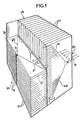
- FIG. 1 shows schematically the opto-electronic spatial switching device according to the invention
- FIG 1 there is illustrated schematically the opto-electronic switching device space according to the invention, applied to the broadcasting of P programs from a group GP of P distinct optical fibers, called program fibers fp, to N subscribers to whom is assigned a group GA of N distinct optical fibers, called fibers of subscribers fa .
- the device comprises a distributor assembly 10 coupled to the ports of the 16 fp program fibers and a geometric selector concentrator assembly 20, subsequently designated more concisely by concentrator-selector, coupled to the distributor assembly 10 and to the ports of the 32 fibers of subscribers fa.
- the distributor assembly 10 is constituted by a stack of 16 optical program distribution plates, 11, each assigned to one of the program fibers fp. These distribution plates 11 are identical to each other. Each of these plates is rigid and flat and incorporates 32 individual waveguides h1 to h32 and has, on one of its edges, a common coupling access of these 32 waveguides with the access of the program fiber fp which is assigned to it, and on the opposite edge, 32 separate so-called exit or distribution accesses of this program arranged in regular steps t.
- the distribution ports on the various plates are on the same side and define between them 32 rows each of 16 distribution ports of the 16 programs, arranged in step r on their row.
- the concentrator-selector assembly 20 is constituted by another stack of 32 concentration and selection plates 21, each assigned to one of the subscriber fibers fa. These concentration and selection plates 21 are identical to each other. Each of them is rigid and flat and incorporates 16 individual waveguides g1 to g16 and has an integrated strip of 16 photodiodes, 31.
- the 16 waveguides g1 to g16 of each of the concentration and selection plates 21 extend into a sheet which opens out from one of the edges of the plate considered, on which they have distinct first ends assembled in line on an extremely small part of this edge, having a very small spacing between them, not indicated in FIG. 1, of the order of 100 ⁇ m, to a second opposite edge of this plate, on which they have second separate ends aligned with each other at regular intervals r of the distribution accesses of the different programs on the rows they define.
- the 16 photodiodes are connected with the first end of the 16 waveguides of this wafer 21 , respectively.
- the integrated strip 31 is secured, by gluing, to the first edge of the wafer by having its individual photodiodes connected to the first ends of the waveguides g, respectively.
- the photodiodes arrays 31 of the different concentration and selection plates 21 are on the same side, while the second ends of their guides g are on the same other opposite side.
- the concentrator-selector assembly 20 and the distributor assembly 10 are assembled by having the 32 concentration and selection plates 21 and the 16 distribution plates 11 arranged orthogonally, with the distribution ports of each of the rows facing the second ends. waveguides g of each of the plates 21.
- Each of the integrated arrays of photodiodes 31 has a common electrical output for the photodiodes of this array. This common output is coupled to the subscriber fiber fa assigned to this concentration and selection wafer 21, by a light-emitting diode, not shown diagrammatically.
- the first elements assigned to subscribers will no longer be optical fibers but electrical conductors.
- the photodiodes arrays will each have their common output connected to the corresponding subscriber conductor.
- the P second elements respectively coupled to the guides of the P distribution plates and formed in the example illustrated by the program fibers fp may be sources of program emitting light, each source being for example constituted by a diode -laser or, more advantageously, of several laser diodes emitting the same program, this latter configuration notably having the advantage, in addition to that of greater reliability, of reducing modal noise thanks to the superposition of the different modes of the lasers.
- each strip will be individually controlled, from the subscriber to whom it corresponds, so that only one of them ensures the transmission of the program transmitted by the only guides g to which it is coupled. From one module to another, these commands are defined from the different subscribers. It follows that the subscribers can receive that of the programs desired among those transmitted, several subscribers being able to receive the same program.
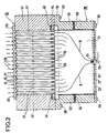
- FIG. 2 a concrete embodiment of the opto-electronic diffuser has been shown, corresponding to that of FIG. 1.
- the identical elements have been identified there by the previous references.
- the stacking of the 16 program distribution plates 11, forming the distributor assembly 10, is carried out between two plates or positioning grids 13 and 14. These grids each have ribs, 15 for the grid 13 and 16 for the grid 14, facing each other from one grid to the other and between which the edges of the distribution plates 11 over which the accesses of their guides extend.
- the ribs 15 between which are received the edges which carry the common coupling ports of the guides of the different plates, to be coupled with the different fibers of program fp, are of rectangular section.
- a window at the bottom of each of the grooves which they define between them allows the coupling of their guides with each of the fibers fp.
- This grid carries elastic tongues 17 which line the bottom of the grooves delimited by the ribs 15, for a positioning without play of the plates 11 on this grid and in the resulting distributor assembly 10.
- the ribs 16 between which are received the edges which carry the program output ports, defined by the guides of each plate 11, have a beveled edge, to allow firm and precise positioning of this edge and therefore of the assembly for the different plates 11.
- the grooves delimited between these ribs 16 are open right through the grid 14, so that the edge of each plate 11 is located in the plane of the flat face of the grid 14.
- Two flanges 41, 42 which may belong to a frame surrounding the stack formed, ensure the assembly of the two grids 13 and 14, the grid edges 14 being received in a recess provided on the internal face of each flange whose bottom carries a bearing 43 or 44, of rubber.
- the grids are fixed to the flanges by screws such as 45, 46.
- the stack of 32 platelets concentration and selection 21 is constituted, in a similar manner, on two grids 23 and 24 similar to the aforementioned grids 13 and 14.
- the grid 23 carries ribs 25, of rectangular section, the grooves of which they delimit are lined with elastic tabs 27. These grooves receive the edges of the plates 21 on which the photodiodes arrays 31 are attached.
- the grid 24 carries ribs 26 having a beveled edge, the grooves of which they delimit receive the edges of the plates carrying the second ends of their guides g.
- Two flanges 51, 52 which may belong to a frame surrounding the stack formed, ensure the assembly of these two grids 23 and 24.
- Each of the opposite edges of the grid 24, transverse to the plates 21, is housed in a recess provided on the internal face of each of the flanges 51, 52. Screws such as 55, 56 maintain the grids on these flanges 51, 52.
- the strip 31 of photodiodes coupled to the guides g, on each of the plates 21, is housed in the thickness of the grid 23, having a window suitable for this purpose.
- the electrical outputs Ca of the various bars emerge from the concentrator-selector assembly 20.
- pairs of adjustment screws such as 47 for the distributor assembly 10 and 53, 54 for the concentrator-selector assembly 20, are mounted to act on the edges of the individual plates free of ends or access to the guides they contain.
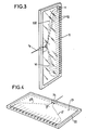
- FIG. 3 an exemplary embodiment of one of the program distribution plates 11 has been illustrated, falling within the embodiments given in FIGS. 1 and 2.
- This plate 11 incorporates the 32 individual guides h1 to h32 illustrated in the figure. 1. These 32 guides have first ends gathered on one edge to constitute the common coupling access of the 32 guides h with the program fiber fp to which the wafer is assigned 11. The 32 guides flourish from this edge where they have their coupling access common with the fiber fp to the opposite edge where they have their other distinct ends, which form the multiple output accesses of this same program, arranged at pitch t between them.
- This plate 11 further comprises a peripheral frame 12, for example of an aluminum-based alloy, for its mechanical mounting in the aforementioned distributor assembly.
- This distribution plate can be produced, in an integrated structure, by creating the waveguides h by diffusion of ions in a glass plate.
- This method of obtaining is described, for example, in the article entitled “Planar multimode devices for fiber optics” by GL Tangonan and others presented at Optical Communication Conference, Amsterdam 17-19, September 1979 or in the article entitled “Fast fabrication method for thick and highly multimode Optical Waveguides "by GH Chartier and others, published in ELECTRONICS LETTERS Vol. 13 No. 25 of December 8, 1977.
- This plate 11 can also be obtained by overmolding of individual fibers constituting said waveguides h in an epoxy resin loaded with siliceous material or by molding these fibers in glass with a melting point of the order of 500 ° and with a low coefficient expansion minimizing stresses during cooling.
- an additional fiber known as a common fiber, with a cross section larger than that of the individual guides, must be added to the 32 individual fibers h in order, on the one hand, to be directly coupled to the corresponding ends of the guides h gathered in a hexagonal network and on the other hand constitute the common coupling access for these 32 guides h with the fiber fp.
- the separate ends of the h guides and the end of the additional common fiber will be initially prepositioned and glued to the frame 12 playing the role of initial positioning frame; after molding or overmolding the edges of this initial frame will be rectified and polished.
- FIG. 4 an exemplary embodiment of one of the plates 21 for concentration and selection has been illustrated, falling within the embodiments given in FIGS. 1 and 2.
- This plate 21 incorporates the 16 individual waveguides g1 to g16 and carries the integrated array of photodiodes 31 attached to its suitable edge.
- the guides g1 to g16 extend from one of its edges where they have their ends widely spaced at pitch r to the opposite edge where they have their other ends brought together, however being distinct and at a small pitch p between they equal to the pitch existing between the photodiodes of the integrated strip 31.
- the strip of photodiodes 31, in which the photodiodes are at pitch p, is bonded to the edge of the wafer 21 opposite these ends of the guides g.
- the plate 21 also further comprises a peripheral frame 22, for its mechanical mounting in the above-mentioned concentrator-selector assembly.
- This concentration and selection plate 21 may be obtained, in a similar manner to the distribution plate, in an integrated structure or starting from individual fibers, which constitute the guides, embedded by molding or overmolding.
- the armature 22 will act as a prepositioning frame for the individual fibers and will have its edges carrying the ends of the rectified and polished fibers.
- the photodiode strip 31 will then be suitably attached to the armature and will be glued to it.
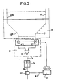
- the optoelectronic diagram defined from one of these concentration and selection plates has been illustrated.
- hx1 to hx16 the guides of the same rank x of the distribution plates whose accesses for the 16 different programs are arranged in a row assigned to the concentration and selection plate 21 illustrated.
- the actual concentration plate with its 16 waveguides g1 to g16 on the one hand coupled to the accesses of the guides hx1 to hxl6, respectively, and on the other hand coupled to the photodiodes d1. to d16 of the integrated bar 31 which it carries.
- the photodiodes have their outputs connected to an amplifier 32 which defines the single output Ca of the strip 31.
- a light-emitting diode Ea ensures the coupling between the output Ca and the subscriber fiber fa.
- These photodiodes d1 to d16 have their individual power supplies from a circuit 60, while an optical coupler 61 inserted on the subscriber fiber fa ensures the selective power supply of one of the photodiodes of the strip, for the selection by this subscriber of the one of the programs transmitted by the individual guides g.
- This optical coupler 61 ensures the continuity of the transmission on the fiber fa of the selected program but also allows the selection of this program from the subscriber fiber. It will include, for example, a semi-transparent mirror interposed between a focusing lens and a collimation lens.
- This selection command, from the subscriber is transmitted by the coupler 61 on a link 62 for controlling the photodiodes supply circuit, after detection not illustrated, the command received allows the supply of only the photodiodes concerned. .
Landscapes
- Physics & Mathematics (AREA)
- General Physics & Mathematics (AREA)
- Optics & Photonics (AREA)
- Optical Couplings Of Light Guides (AREA)
- Use Of Switch Circuits For Exchanges And Methods Of Control Of Multiplex Exchanges (AREA)
- Optical Communication System (AREA)
Applications Claiming Priority (2)
| Application Number | Priority Date | Filing Date | Title |
|---|---|---|---|
| FR8308971 | 1983-05-31 | ||
| FR8308971A FR2547071B1 (fr) | 1983-05-31 | 1983-05-31 | Dispositif opto-electronique de commutation spatiale |
Publications (2)
| Publication Number | Publication Date |
|---|---|
| EP0131722A1 EP0131722A1 (fr) | 1985-01-23 |
| EP0131722B1 true EP0131722B1 (fr) | 1987-07-22 |
Family
ID=9289330
Family Applications (1)
| Application Number | Title | Priority Date | Filing Date |
|---|---|---|---|
| EP84106108A Expired EP0131722B1 (fr) | 1983-05-31 | 1984-05-29 | Dispositif opto-électronique de commutation spatiale |
Country Status (7)
| Country | Link |
|---|---|
| US (1) | US4653850A (enExample) |
| EP (1) | EP0131722B1 (enExample) |
| JP (1) | JPS6011822A (enExample) |
| CA (1) | CA1196383A (enExample) |
| DE (1) | DE3464973D1 (enExample) |
| FR (1) | FR2547071B1 (enExample) |
| IE (1) | IE55253B1 (enExample) |
Cited By (1)
| Publication number | Priority date | Publication date | Assignee | Title |
|---|---|---|---|---|
| DE4009323C1 (enExample) * | 1990-03-23 | 1991-02-21 | Ant Nachrichtentechnik Gmbh, 7150 Backnang, De |
Families Citing this family (26)
| Publication number | Priority date | Publication date | Assignee | Title |
|---|---|---|---|---|
| DE3138686A1 (de) * | 1981-09-29 | 1983-04-14 | Siemens AG, 1000 Berlin und 8000 München | Schalter fuer lichtleiter |
| DE3587515T2 (de) * | 1984-05-17 | 1994-03-17 | Nippon Electric Co | Optische Schalteinrichtung. |
| US4730893A (en) * | 1985-07-26 | 1988-03-15 | Siemens Aktiengesellschaft | Support assembly for light waveguide couplings |
| JPH01177508A (ja) * | 1988-01-07 | 1989-07-13 | Furukawa Electric Co Ltd:The | 光スイッチ |
| CA1321089C (en) * | 1988-05-06 | 1993-08-10 | Adc Telecommunications, Inc. | Optical switch |
| US4943136A (en) * | 1988-12-09 | 1990-07-24 | The Boeing Company | Optical backplane interconnection |
| JP2718013B2 (ja) * | 1989-01-12 | 1998-02-25 | 住友電気工業株式会社 | 光ファイバ配線装置 |
| GB2239323A (en) * | 1989-12-21 | 1991-06-26 | Plessey Co Plc | Optical waveguide stacks and assemblies connected to opto-electronic components |
| SE465235B (sv) * | 1989-12-21 | 1991-08-12 | Ericsson Telefon Ab L M | Fiberoptisk vaexel |
| US5155785A (en) * | 1991-05-01 | 1992-10-13 | At&T Bell Laboratories | Optical fiber interconnection apparatus and method |
| US5463704A (en) * | 1994-05-16 | 1995-10-31 | Adc Telecommunications, Inc. | Fiber optic switch |
| US5455878A (en) * | 1994-08-15 | 1995-10-03 | The Boeing Company | Programmable signal time delay device using electro-optic and passive waveguide circuits on planar substrates |
| US5729642A (en) * | 1995-10-02 | 1998-03-17 | The Boeing Company | N×N optical switch array using electro-optic and passive waveguide circuits on planar substrates |
| US5734764A (en) * | 1996-09-10 | 1998-03-31 | International Business Machines Corporation | Method and apparatus for achieving a fully-connected nonblocking optical crossbar switch having wide transfer paths and minimal latency by exploiting the transparency of silicon at selected wavelengths |
| US5841917A (en) * | 1997-01-31 | 1998-11-24 | Hewlett-Packard Company | Optical cross-connect switch using a pin grid actuator |
| US7167615B1 (en) | 1999-11-05 | 2007-01-23 | Board Of Regents, The University Of Texas System | Resonant waveguide-grating filters and sensors and methods for making and using same |
| US6594437B1 (en) | 2000-08-15 | 2003-07-15 | Fci Americas Technology, Inc. | Optical fiber separation and regrouping device |
| US6819821B2 (en) * | 2002-03-26 | 2004-11-16 | Agilent Technologies, Inc. | Optical switch with a geometry based on perpendicularly-oriented planar lightwave circuit switches |
| US9261556B2 (en) | 2013-06-10 | 2016-02-16 | Freescale Semiconductor, Inc. | Optical wafer and die probe testing |
| US9435952B2 (en) | 2013-06-10 | 2016-09-06 | Freescale Semiconductor, Inc. | Integration of a MEMS beam with optical waveguide and deflection in two dimensions |
| US9094135B2 (en) * | 2013-06-10 | 2015-07-28 | Freescale Semiconductor, Inc. | Die stack with optical TSVs |
| US10230458B2 (en) | 2013-06-10 | 2019-03-12 | Nxp Usa, Inc. | Optical die test interface with separate voltages for adjacent electrodes |
| US9442254B2 (en) | 2013-06-10 | 2016-09-13 | Freescale Semiconductor, Inc. | Method and apparatus for beam control with optical MEMS beam waveguide |
| US9810843B2 (en) | 2013-06-10 | 2017-11-07 | Nxp Usa, Inc. | Optical backplane mirror |
| US9091820B2 (en) * | 2013-06-10 | 2015-07-28 | Freescale Semiconductor, Inc. | Communication system die stack |
| US9766409B2 (en) | 2013-06-10 | 2017-09-19 | Nxp Usa, Inc. | Optical redundancy |
Family Cites Families (12)
| Publication number | Priority date | Publication date | Assignee | Title |
|---|---|---|---|---|
| US3542451A (en) * | 1969-06-06 | 1970-11-24 | Bausch & Lomb | Wear-resistant encapsulated fiber optical assembly |
| US3792239A (en) * | 1971-12-30 | 1974-02-12 | Northern Illinois Gas Co | Device for transmitting wavelengths of the electromagnetic spectrum |
| GB1407544A (en) * | 1973-03-01 | 1975-09-24 | Standard Telephones Cables Ltd | Optical coupler |
| US3920982A (en) * | 1974-02-08 | 1975-11-18 | Us Navy | Continuous fiber optical transmit and receive terminal |
| US3977762A (en) * | 1974-09-05 | 1976-08-31 | International Standard Electric Corporation | Optical coupler |
| DE2523496A1 (de) * | 1975-05-27 | 1976-12-16 | Max Planck Gesellschaft | Optische vorrichtung zur uebertragung von informationen |
| US4070093A (en) * | 1976-08-26 | 1978-01-24 | Bell Telephone Laboratories, Incorporated | Minimizing transmission path disabling due to defective transmission members of a communications cable |
| FR2512620B2 (fr) * | 1981-02-13 | 1988-02-05 | France Etat | Concentrateur-distributeur optique matriciel |
| US4444458A (en) * | 1981-05-26 | 1984-04-24 | Gould Inc. | Substrate ruggedized optical fiber apparatus |
| FR2520179A1 (fr) * | 1982-01-20 | 1983-07-22 | Comp Generale Electricite | Dispositif de commutation en cascade par flexion de fibres optiques pour reseau de transmission d'informations |
| NL8204722A (nl) * | 1982-12-07 | 1984-07-02 | Philips Nv | Distributiesysteem voor lokaal fibernet. |
| JPH1125A (ja) * | 1997-06-12 | 1999-01-06 | Seirei Ind Co Ltd | 走行式茎処理機の茎処理機構 |
-
1983
- 1983-05-31 FR FR8308971A patent/FR2547071B1/fr not_active Expired
-
1984
- 1984-05-29 DE DE8484106108T patent/DE3464973D1/de not_active Expired
- 1984-05-29 EP EP84106108A patent/EP0131722B1/fr not_active Expired
- 1984-05-30 US US06/615,449 patent/US4653850A/en not_active Expired - Fee Related
- 1984-05-30 IE IE1359/84A patent/IE55253B1/en not_active IP Right Cessation
- 1984-05-30 CA CA000455427A patent/CA1196383A/fr not_active Expired
- 1984-05-31 JP JP59112173A patent/JPS6011822A/ja active Granted
Cited By (1)
| Publication number | Priority date | Publication date | Assignee | Title |
|---|---|---|---|---|
| DE4009323C1 (enExample) * | 1990-03-23 | 1991-02-21 | Ant Nachrichtentechnik Gmbh, 7150 Backnang, De |
Also Published As
| Publication number | Publication date |
|---|---|
| EP0131722A1 (fr) | 1985-01-23 |
| IE841359L (en) | 1984-11-30 |
| CA1196383A (fr) | 1985-11-05 |
| FR2547071A1 (fr) | 1984-12-07 |
| FR2547071B1 (fr) | 1986-02-14 |
| JPH0446510B2 (enExample) | 1992-07-30 |
| DE3464973D1 (en) | 1987-08-27 |
| JPS6011822A (ja) | 1985-01-22 |
| IE55253B1 (en) | 1990-07-18 |
| US4653850A (en) | 1987-03-31 |
Similar Documents
| Publication | Publication Date | Title |
|---|---|---|
| EP0131722B1 (fr) | Dispositif opto-électronique de commutation spatiale | |
| EP0127871B1 (fr) | Ensemble de commutation optique spatiale | |
| US10545300B2 (en) | Three-dimensional WDM with 1×M output ports on SOI based straight waveguides combined with wavelength filters on 45 degree reflectors | |
| US6021238A (en) | Optoelectronic module for bidirectional optical data transmission | |
| EP0537046A2 (fr) | Ensemble d'interconnexion optique pour cartes électroniques | |
| US20050069013A1 (en) | Method and apparatus for wavelength division multiplexing | |
| EP0860724A1 (fr) | Procédé d'assemblage d'un dispositif opto-hybride | |
| US20180275347A1 (en) | Compact structure of integrated WDM device | |
| WO2003060584A1 (en) | Optical waveguide module | |
| US6028708A (en) | Method for producing a beam splitter molded part and optoelectronic module using the beam splitter molded part | |
| JP2001501378A (ja) | 双方向光データ伝送のためのオプトエレクトロニックモジュール | |
| EP0881527B1 (fr) | Système de commutation optique spatiale à déflecteur acousto-optique multicanaux | |
| JPH09281302A (ja) | 反射面付き平板マイクロレンズアレイおよびその製造方法 | |
| CA2282938A1 (fr) | Dispositif de regeneration d'un signal multiplexe en longueurs d'onde comprenant un absorbant saturable | |
| EP0131131B1 (fr) | Ensemble de commutation optique spatiale | |
| JP3275864B2 (ja) | 光半導体装置及びその製造方法 | |
| EP0166291A1 (fr) | Dispositif de distribution d'energie lumineuse et son utilisation a la commutation optique | |
| EP1459118A1 (fr) | Dispositif de multiplexage d'une matrice de voies optiques, application au multiplexage en longueur d'onde et a l'insertion-extraction | |
| FR2829246A1 (fr) | Structure d'absorbant optique saturable et dispositif de regeneration d'un signal multiplexe en longueurs d'onde l'incorporant | |
| JPS62217226A (ja) | 光制御装置 | |
| JP2956332B2 (ja) | 光半導体モジュール | |
| FR2798010A1 (fr) | Composant electro-optique multi-sections | |
| JP3535655B2 (ja) | 光モジュール、その連結方法 | |
| FR2529687A1 (fr) | Dispositif de commutation optique | |
| FR2500247A1 (fr) | Concentrateur-distributeur optique matriciel |
Legal Events
| Date | Code | Title | Description |
|---|---|---|---|
| PUAI | Public reference made under article 153(3) epc to a published international application that has entered the european phase |
Free format text: ORIGINAL CODE: 0009012 |
|
| AK | Designated contracting states |
Designated state(s): BE DE FR GB IT LU NL SE |
|
| 17P | Request for examination filed |
Effective date: 19850716 |
|
| RAP1 | Party data changed (applicant data changed or rights of an application transferred) |
Owner name: ALCATEL |
|
| 17Q | First examination report despatched |
Effective date: 19860919 |
|
| RAP1 | Party data changed (applicant data changed or rights of an application transferred) |
Owner name: ALCATEL CIT |
|
| GRAA | (expected) grant |
Free format text: ORIGINAL CODE: 0009210 |
|
| AK | Designated contracting states |
Kind code of ref document: B1 Designated state(s): BE DE FR GB IT LU NL SE |
|
| REF | Corresponds to: |
Ref document number: 3464973 Country of ref document: DE Date of ref document: 19870827 |
|
| ITF | It: translation for a ep patent filed | ||
| PLBE | No opposition filed within time limit |
Free format text: ORIGINAL CODE: 0009261 |
|
| STAA | Information on the status of an ep patent application or granted ep patent |
Free format text: STATUS: NO OPPOSITION FILED WITHIN TIME LIMIT |
|
| 26N | No opposition filed | ||
| PGFP | Annual fee paid to national office [announced via postgrant information from national office to epo] |
Ref country code: LU Payment date: 19910607 Year of fee payment: 8 |
|
| EPTA | Lu: last paid annual fee | ||
| PG25 | Lapsed in a contracting state [announced via postgrant information from national office to epo] |
Ref country code: LU Free format text: LAPSE BECAUSE OF NON-PAYMENT OF DUE FEES Effective date: 19920529 |
|
| PGFP | Annual fee paid to national office [announced via postgrant information from national office to epo] |
Ref country code: GB Payment date: 19930422 Year of fee payment: 10 |
|
| PGFP | Annual fee paid to national office [announced via postgrant information from national office to epo] |
Ref country code: DE Payment date: 19930519 Year of fee payment: 10 |
|
| PGFP | Annual fee paid to national office [announced via postgrant information from national office to epo] |
Ref country code: SE Payment date: 19930521 Year of fee payment: 10 |
|
| PGFP | Annual fee paid to national office [announced via postgrant information from national office to epo] |
Ref country code: FR Payment date: 19930527 Year of fee payment: 10 |
|
| ITTA | It: last paid annual fee | ||
| PGFP | Annual fee paid to national office [announced via postgrant information from national office to epo] |
Ref country code: NL Payment date: 19930531 Year of fee payment: 10 |
|
| PGFP | Annual fee paid to national office [announced via postgrant information from national office to epo] |
Ref country code: BE Payment date: 19930616 Year of fee payment: 10 |
|
| PG25 | Lapsed in a contracting state [announced via postgrant information from national office to epo] |
Ref country code: GB Effective date: 19940529 |
|
| PG25 | Lapsed in a contracting state [announced via postgrant information from national office to epo] |
Ref country code: SE Effective date: 19940530 |
|
| PG25 | Lapsed in a contracting state [announced via postgrant information from national office to epo] |
Ref country code: BE Effective date: 19940531 |
|
| BERE | Be: lapsed |
Owner name: ALCATEL CIT Effective date: 19940531 |
|
| PG25 | Lapsed in a contracting state [announced via postgrant information from national office to epo] |
Ref country code: NL Effective date: 19941201 |
|
| NLV4 | Nl: lapsed or anulled due to non-payment of the annual fee | ||
| GBPC | Gb: european patent ceased through non-payment of renewal fee |
Effective date: 19940529 |
|
| EUG | Se: european patent has lapsed |
Ref document number: 84106108.8 Effective date: 19941210 |
|
| PG25 | Lapsed in a contracting state [announced via postgrant information from national office to epo] |
Ref country code: FR Effective date: 19950131 |
|
| PG25 | Lapsed in a contracting state [announced via postgrant information from national office to epo] |
Ref country code: DE Effective date: 19950201 |
|
| EUG | Se: european patent has lapsed |
Ref document number: 84106108.8 |
|
| REG | Reference to a national code |
Ref country code: FR Ref legal event code: ST |