EP0131440B1 - TSF-système électronique de surveillance avec fréquence variable - Google Patents
TSF-système électronique de surveillance avec fréquence variable Download PDFInfo
- Publication number
- EP0131440B1 EP0131440B1 EP84304615A EP84304615A EP0131440B1 EP 0131440 B1 EP0131440 B1 EP 0131440B1 EP 84304615 A EP84304615 A EP 84304615A EP 84304615 A EP84304615 A EP 84304615A EP 0131440 B1 EP0131440 B1 EP 0131440B1
- Authority
- EP
- European Patent Office
- Prior art keywords
- frequencies
- frequency
- bursts
- resonant
- generating
- Prior art date
- Legal status (The legal status is an assumption and is not a legal conclusion. Google has not performed a legal analysis and makes no representation as to the accuracy of the status listed.)
- Expired
Links
Images


Classifications
-
- G—PHYSICS
- G08—SIGNALLING
- G08B—SIGNALLING OR CALLING SYSTEMS; ORDER TELEGRAPHS; ALARM SYSTEMS
- G08B13/00—Burglar, theft or intruder alarms
- G08B13/22—Electrical actuation
- G08B13/24—Electrical actuation by interference with electromagnetic field distribution
- G08B13/2402—Electronic Article Surveillance [EAS], i.e. systems using tags for detecting removal of a tagged item from a secure area, e.g. tags for detecting shoplifting
- G08B13/2405—Electronic Article Surveillance [EAS], i.e. systems using tags for detecting removal of a tagged item from a secure area, e.g. tags for detecting shoplifting characterised by the tag technology used
- G08B13/2414—Electronic Article Surveillance [EAS], i.e. systems using tags for detecting removal of a tagged item from a secure area, e.g. tags for detecting shoplifting characterised by the tag technology used using inductive tags
-
- G—PHYSICS
- G08—SIGNALLING
- G08B—SIGNALLING OR CALLING SYSTEMS; ORDER TELEGRAPHS; ALARM SYSTEMS
- G08B13/00—Burglar, theft or intruder alarms
- G08B13/22—Electrical actuation
- G08B13/24—Electrical actuation by interference with electromagnetic field distribution
- G08B13/2402—Electronic Article Surveillance [EAS], i.e. systems using tags for detecting removal of a tagged item from a secure area, e.g. tags for detecting shoplifting
- G08B13/2428—Tag details
- G08B13/2431—Tag circuit details
-
- G—PHYSICS
- G08—SIGNALLING
- G08B—SIGNALLING OR CALLING SYSTEMS; ORDER TELEGRAPHS; ALARM SYSTEMS
- G08B13/00—Burglar, theft or intruder alarms
- G08B13/22—Electrical actuation
- G08B13/24—Electrical actuation by interference with electromagnetic field distribution
- G08B13/2402—Electronic Article Surveillance [EAS], i.e. systems using tags for detecting removal of a tagged item from a secure area, e.g. tags for detecting shoplifting
- G08B13/2465—Aspects related to the EAS system, e.g. system components other than tags
- G08B13/2488—Timing issues, e.g. synchronising measures to avoid signal collision, with multiple emitters or a single emitter and receiver
Definitions
- This invention relates to radio frequency (RF) electronic article surveillance systems in which markers having circuits resonant at a desired frequency are used.
- the present invention relates to such systems in which pulses of RF energy are transmitted into an interrogation zone and energy absorbed by the marker circuit is transmitted at its resonant frequency and is detected during quiescent intervals between the transmitted pulses.
- RF radio frequency
- a pulsed system such as described above is disclosed by Thompson (U.S. Patent No. 3,740,742).
- the primary advantage of such a system is that it is much easier to detect the relatively weak signals generated by the marker circuit in the absence of much stronger fields produced by the transmitter.
- Other techniques for detecting the weaker marker signals over the much more intense transmitted signals include the detection of signals at frequencies other than that originally transmitted, such as by use of a marker which generates harmonics of the transmitted frequency.
- it is known to sweep the transmitted energy over a range of frequencies encompassing the resonant frequency of the marker circuit such that the marker may be detected by conventional grid-dip techniques.
- the system of the present invention is predicated on the assumption that the marker is to be disposable, and hence is very inexpensive. Such low cost further virtually dictates that manufacturing tolerances on the marker circuit be loose and precludes anything close to 100% testing of the circuits to enable sorting the circuits according to discrete resonant frequencies. Notwithstanding the above, such loose tolerance marker circuits are desirably used in antipilferage applications where the concern of merchants over possible false alarms, and customer ill-will are paramount.
- the apparatus of the present invention is for detecting in an interrogation zone, articles having affixed thereto markers containing circuits each resonant at a frequency within a predetermined range of frequencies and having a bandwidth centered about said resonant frequency, said apparatus comprising transmitter means for generating in the interrogation zone short bursts of electromagnetic field energy, the burst being separated by quiescent periods and receiver means for detecting electromagnetic energy during the quiescent periods.
- the transmitter means creates within an interrogation zone bursts of electromagnetic energy at discretely different radio frequencies (RF) within a predeterminred range of frequencies, each burst being spatially separated from the next by a quiscent period during which the transmitter does not transmit, and the receiver means receives electromagnetic signals at the radio frequencies during the quiescent periods and activates an alarm when the received signals exceed a predetermined level.
- RF radio frequencies
- the markers adapted to be affixed to articles to be monitored within the interrogation zone each comprise an inductive- capacitance (LC) circuit resonant at a frequency within the range of transmitted frequencies such that when the market is in the interrogation zone, RF transmitted energy is absorbed by the LC circuit and is reemitted at its resonant frequency during the subsequent quiescent period for receipt by the receiver.
- LC inductive- capacitance
- the apparatus of the present invention is characterised by transmitter means including means for generating said interrogation signal said bursts at a sufficient number of discrete, different RF frequencies to provide bursts of at least three different frequencies within the bandwidth of each of said resonant circuits, said bursts being separated by quiescent periods, and by said receiver means including means for actuating an alarm in response to the detection of energy at least three frequencies within said predetermined range during periods following pulses.
- the receiver comprises means at least responsive to frequencies extending through the bandwidth (BW) of all of the LC circuits for activating an alarm signal when signals exceeding a predetermined level and corresponding to at least three frequencies are detected, i.e. when a LC circuit is activated by at least three frequencies.
- BW bandwidth
- the marker circuits are designed to have a Q-factor in the range of 70-100.
- Analogously preferred marker circuits desirably have a bandwidth (BW) in the range of 20-100 KHz, such that at a Q-factor of at least 50, the nominal resonant frequency must be greater than a range of frequencies between 1-5 MHz.
- the marker circuits are designed to resonate at a specific frequency with a predetermined frequency range ( ⁇ f) ⁇ of the nominal resonant frequency, such as for example within ⁇ 10%.
- the transmitter thus also includes means for generating bursts of a plurality of different RF frequencies extending over a range at least as wide as the sum of ⁇ f+BW max , where BW max is the broadest bandwidth of any of the LC circuits.
- BW max is the broadest bandwidth of any of the LC circuits.
- the transmitter preferably creates bursts at frequencies which are incrementally different fcmm the next closest frequency by not more than one-third the narrowest bandwidth (BW mln ) of any of the LC circuits.
- Such bursts are further desirably spaced at increments and include as many discrete frequencies as are determined by the expression where Q max is the highest Q-factor and f min is the minimum resonant frequency of any of the LC circuits.
- the receiver of the present system is provided with additional features to enhance accurate detection of the LC circuits.
- the receiver desirably responds to received signals extending over only a limited frequency range and is tuned to maintain its limited frequency response centered on the transmitted frequency.
- the receiver preferably includes means activated during a first interval of time relatively early in each of the quiescent periods for comparing received signals believed to be produced by resonating circuits with signals representative of background noise in order to enhance signal discrimination.
- Such means are initially activated during a first interval of time relatively early in each of the quiescent periods when a signal produced by a resonating marker circuit would likely be present for providing a marker signal in response to electromagnetic signals received during that interval.
- Means are subsequently activated during a second interval of time occurring relatively later in each of the quiescent periods when no signals produced by resonating marker circuits would likely be present, for providing a noise signal in response to signals received during the second interval. In the event the marker signal exceeds the noise signal by a predetermined amount, a detector signal is then provided.
- the transmitter provides a number of bursts at each discrete frequency, with a quiescent period between each burst and repeats the repetitive bursts at all of the different discrete frequencies in consecutive sequences.
- the receiver then also desirably accumulates marker and noise signals provided following each burst at a single frequency to create a detector signal corresponding to that frequency if the accumulated marker signals at that frequency exceed the corresponding accumulated noise signals.
- Such accumulation is preferably repeated for the received marker and noise signals corresponding to each discrete frequency to create detector signals corresponding to all frequencies, which signals may, for example, result from an analog comparator which provides a high state only when the accumulated amplitude of the marker signals received following bursts at a single frequency exceed the accumulated amplitude of the corresponding noise signals.
- the detector signals are in turn desirably stored, such as in a shift register, to enable comparison of those signals received during one sequence with those produced in a subsequent sequence.
- the comparison is preferably performed to determine the presence of detector signals corresponding to three adjacent frequencies in two consecutive sequences, and in that event, a prealarm signal is produced.
- the prealarm signal is preferably inhibited from producing an alarm signal if detector signals are detected which correspond to more than a limited number of discrete frequencies, such as a selected number of adjacent frequencies within the bandwidths of one, or at most, a few marker circuits such as could be within an interrogation zone at a given time.
- Such an inhibition circuit thus prevents the presence of a low Q circuit having an appropriate resonant frequency from falsely resulting in an alarm signal.
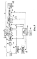
- the system of the present invention preferably includes a transmitter section 10, a receiver section 12, and at-least one marker 14.
- the transmitter portion 10 includes a voltage controlled oscillator 16 which produces repetitive sequences of oscillations at each of the discrete frequencies provided in the present system. These sequences are applied to an amplifier stage 18 which both amplifies and switches each of the discrete frequencies to provide bursts with a quiescent period between each burst.
- the output of the amplifier 18 is coupled to an antenna tuning stage 20 which is used to tune the transmit antenna 22.
- the transmit antenna 22 as well as a receive antenna 24 are positioned within a single enclosure 26, desirably located on one side of an interrogation zone. RF energy provided within the zone by the transmit antenna 22 is radiated so as to energize a marker 14 when present within the zone.
- the marker includes at least one tuned resonant circuit 28, including an inductor 30 and a capacitor 32. Energy transmitted via the transmitting antenna 22 having a frequency within the bandwidth of the resonant circuit 28 will be absorbed by that circuit and reradiated during the quiescent period between each transmitted burst. The reradiated energy will be received by the receive antenna 24 and further processed within the receiver 12.
- the receiver of Figure 1 may further be seen to include an antenna tuning stage 34, an amplifier 36, an integrator/comparator 38, a detector 40, and an alarm circuit 42.
- Signals provided via the receive antenna 24 are coupled into the antenna tuning network 34, which has a narrow bandwidth, and is tracked to pass the same frequency as that being transmitted via the transmitter 10. Such frequencies are then coupled to the amplifier 36 and the output thereof processed so as to distinguish signals produced by a resonant circuit 28 within the interrogation zone from background noise.
- Appropriately processed detector signals are coupled to the detector 40 where additional processing is provided to provide an unambiguous alarm signal which is coupled to the alarm circuit 42.
- a time control generator 44 which is driven by a crystal controlled clock 46, a staircase generator 48 and a staircase adjust circuit 50.
- the time control generator provides appropriately timed control pulses to the respective portions of the transmitter and receiver, while the staircase generator generates appropriate voltage ramps utilized in providing the plurality of discrete frequencies in the voltage controlled oscillator 16 as well as in controlling the antenna tuning within the receiver.
- Te pictorial view of a preferred sequence of frequencies such as is transmitted via the transmit antenna into the interrogation zone is shown in Figure 2.
- each frequency is transmitted as repetitive bursts, each burst being separated by a quiescent period.
- the transmit frequency is centered about 4.5 MHz
- incremental frequencies may be provided at approximately 4.48, 4.49, 4.50, 4.51, and 4.52 MHz.
- the transmitted energy at each of the frequencies includes eight bursts, each burst extending approximately 20 microseconds, followed by a 28 microsecond quiescent period. The succession of eight such burst thus extends approximately 384 microseconds.
- the transmitted frequencies extend over a predetermined range.
- the range may extend over ⁇ 10% of the center transmitted frequency of 4.5 MHz.
- Such a range may extend from 4.05 to 4.96 MHz.
- the predetermined range of frequencies may be somewhat less, for example, extending between 4.2 through 4.8 MHz, and include 64 discrete incremental frequencies, there being a 9.4 kHz separation between each adjacent frequency.
- Such a range of frequencies and duration of each transmitted burst thus complies with FCC limits on transmitted sweep rates, while enabling reliable detection of a resonant circuit.
- transmit enable pulses are applied to the amplifier 18 so as to switch each frequency as provided by the voltage controlled oscillator 16 into a series of eight bursts, burst 1, 2 and 8 of which are shown.
- Each high state of the transmit enable signal (curve A) is 20 microseconds in duration, while the low state or quiescent period following each high state is 28 microseconds in duration.
- the transmit enable pulses thus result in transmitted energy being provided via the transmit antenna 22 in the form of radiated bursts as shown in Curve B.
- the oscillations are shown to gradually build up during each transmit enable period and upon cessation of that period to exponentially decrease in intensity, and during most of the quiescent period no energy is being transmitted.
- Transmitted energy at or near the resonant frequency of a resonant circuit 28 will thus cause energy to be absorbed by the circuit as shown in Curve C.
- the absorbed energy is reemitted, such emission persisting after cessation of the transmitted pulses, and extending during an appreciable portion of each quiescent period.
- Curve D represents receiver mute pulses which are applied to the antenna tuning and amplifier portions 34 and 36 respectively of the receiver 12 shown in Figure 1. When the mute pulses are in a high state the antenna tuning and amplifier stages are deactivated and thus prevent energy produced during the transmit cycle from being received.
- the antenna tuning and amplifier stages are activated, thus enabling the decaying energy provided in the marker responses to be detected.
- the receiver mute pulses (Curve D) are slightly longer in duration than the transmit enable pulses A, thereby ensuring that the receiver sections are not activated until all of the transmitted energy has decayed as shown in Curve B.
- the output of the amplifier 36 (Curve D) essentially comprises signals corresponding to the portion of the marker response signals C remaining after the receiver mute pulses (Curve D) are in a low state.
- the integrator/comparator network 38 separates each quiescent period into two portions, a first portion occurring relatively early during each quiescent period and which corresponds to the time during which signals provided by a resonant circuit would be expected to be present, and a second portion, occurring late during each quiescent period during which no marker signal would be expected to be present and which would represent background noise.
- Each of these two portions are enabled by appropriate pulses, shown in Figure 3 as a marker window pulse (Curve F) and noise window pulse (Curve G). It will thus be seen in Figure 3 that the marker window pulses (Curve F) occur while the receiver pulses still have appreciable amplitude.
- the integrator/comparator network 38 includes a pair of integrators, one being actiated by the marker window pulses to integrate marker signals received during a predetermined number of successive quiescent periods, and the second being activated by the noise integrator pulses to integrate the background noise signals received during the same successive quiescent periods.
- the successive periods are desirably those corresponding to each individual frequency, such as namely the eight successive bursts, discussed above, three of which are shown in Figure 3.
- an integrator reset pulse (Curve K) is provided to reset both the integrators and reestablish a zero integration level as shown in Curves H and I. Accordingly, during each eight successive quiescent periods, and during each of the respective marker and time windows, the marker integrator and noise integrator will accumulate signal levels as shown in Curves H and I respectively.
- the comparator sample pulse (Curve J) the relative levels in each of the integrators are compared within the comparator portion of the network 38 and an appropriate output signal produced.
- the generator of the respective timing signals shown in Figure 3 within the time control generator 44 of Figure 1 are accomplished by circuits well known to those skilled in the art.
- the clock 46 of Figure 1 is a crystal controlled oscillator having a base frequency of 1 . MHz. These clock pulses are acted upon within the time control generator 44 by appropriate shift registers, counters and the like to provide the respective pulses as shown in Figure 3.
- the staircase generator 48 is formed of a digital counter 52 and a digital to analog (D/A) converter 54. Appropriate pulses from the time control generator 44 are accumulated within the counter 52 until counts corresponding to a time duration of 384 microseconds have been accumulated. This count is then converted via the converter 54 into an analog level having a 384 microsecond duration. Similarly, the counter continues to count for successive 384 microsecond intervals, and supplies a new analog level to the D/A converter 54 during each of such intervals to generate a staircase ramp, each level in the staircase lasting 384 microseconds, there being 64 such levels in the ramp. At the end of such a sequence the counter is reset so as to begin a second identical sequence, each sequence thus lasting 24.576 milliseconds.
- the produced staircase is shown as Curve L in Figure 7.
- the respective amplitudes of the staircase signal is adjusted in the network 50 and one output therefrom provided on lead 56 to the voltage controlled oscillator network 58.
- a commercial integrated circuit such as type MC 1648 manufactured by Motorola.
- Such a circuit converts the staircase voltage signal provided via the staircase adjust network 50 into a plurality of discrete frequencies centered about a given frequency, as dictated by a resonant circuit. In a preferred embodiment, such a center frequency may be 4.5 MHs, and the range of discrete frequencies extending between 4.2 and 4.8 MHz. Continuous bursts of each of the discrete frequencies are thus provided on lead 60, to a Class A amplifier 62. Signals outputted from that amplifier are in turn coupled to a driver Class A amplifier 64.
- Both the amplifiers 62 and 64 are in turn activated by the transmitter enable pulses (Curve A of Figure 3), thus switching the continuous oscillations at each of the discrete frequencies into the succession of 20 microsecond bursts, each burst being followed by a 28 microsecond quiescent period, thereby forming the staircase of discrete frequencies, as shown in Figure 2.
- Such a signal is then coupled to the Class C power amplifier 65 and the output therefrom provided to the transmitter antenna 22.
- the antenna is desirably tuned to match the frequency to be transmitted.
- the antenna tuning network 20 encompasses four tuning stages, a primary tuning stage 66 (band 4) and three secondary turning stage 68, 70 and 72. (Bands 1, 2 and 3 respectively).
- the VCO 58 and first amplifier 62 are both a portion of a single integrated circuit such as a Motorola type MC1648.
- the amplifiers 62 and 64 are activated by means of solid state switches 74 and 76 respectively under control of the transmit enable pulses (Curve A of Figure 3) provided from the time control generator 44.
- the frequency of the oscillations provided by the VCO 58 is controlled by a resonant inductor/ capacitor network 78.
- This network includes an inductor 80 and capacitors 82, 84, 86 and 88, and varactor diode 90.
- the varactor 90 the capacitance of which is an inverse function of the voltage applied thereto.
- the resonant frequency of the inductor/capacitor network 78 is an inverse function of the inductance and capacitance of the circuit, the resonant frequency will increase with increasing voltage applied at terminal 92. Accordingly, by the application of a voltage staircase such as Curve L shown in Figure 7, together with the transmitter enable pulses (Curve A) the VCO network 16 provides the appropriate succession of bursts at the desired discrete different frequencies on output lead 94.
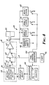
- the antenna tuning network 20 shown in Figures 1 and 4 is shown in Figure 6.
- the output signal provided from the VCO network 16 on lead 94 is coupled to the power amplifier 65 and the amplified output therefrom to the transmit antenna 22.
- the antenna is desirably is in the form of an inductive winding, and preferably includes at least one twisted loop such as disclosed in U.S. Patent No. 4,251,808 (Lichtblau).
- the antenna 22 forms the inductive component of a resonant circuit, the other component being formed via one of a number of parallel capacitors made up within the tuning stages 66, 68, 70 and 72 respectively.
- the fundamental tuning of the transmitting antenna is thus provided by the capacitor 95 within the primary tuning stage 66.
- capacitor 96 within the first stage 68 is coupled to the primary stage the capacitor upon energization of the PIN diode 98.
- the energization of the PIN diode 98 is enabled through a feed choke 100 in response to a control pulse (Curve M of Figure 7) applied thereto.
- the second stage 70 similarly comprise a capacitor 102 which is selectively coupled to ground through PIN diode 104 which in turn may be placed in its conductive state via a pulse (Curve N in Figure 7) provided through the choke 106.
- the capacitor 108 within the third stage 72 may similarly be coupled to ground via PIN diode 110 which in turn is placed in its conductive state by a pulse (Curve O shown in Figure 7) applied through a feed choke 112.
- Each of the frequency bands are desirably designed to encompass a band of frequencies.
- Figure 8 pictorially illustrates the desired frequency bands encompassed by each of the circuits.
- the primary tuning band 66 corresponds to the highest frequency, shown as Curve 114 in Figure 8, whereas the frequency resulting upon energization of the first stage 68 is shown as Curve 116, that produced upon energization of the second stage 70 is shown as Curve 118, and that provided upon energization of the third stage 72 is shown as Curve 120.
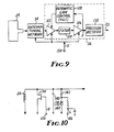
- antenna tuning network 34 and amplifier 36 within the receiver section 12 Details of the antenna tuning network 34 and amplifier 36 within the receiver section 12 are provided in Figures 9 and 10. Particularly as shown in Figure 9, electromagnetic signals received via the antenna 24 and coupled through the antenna tuning network 34 are amplified and rectified within the amplifier 36. That amplifier includes a preamplifier 122, a band pass filter 124, an amplifier 126, and an automatic gain control (AGG) network 128.
- AAG automatic gain control
- receiver mute pulses (Curve D of Figure 3) are applied at terminal 130, and are used in an inverted manner to that shown in conjunction with the transmit enable pulses applied to the amplifiers 62 and 64 in Figure 4 to disable the amplifiers 122 and 126 when the receiver mute pulses are high, thereby enabling signals to pass through those amplifiers only when the receiver mute pulses are in a low state.
- the amplifiers 122 and 126 are of conventional design to give appropriate gain. Amplified signals passing through the preamplifier 122 are acted upon within band pass filter 124 to remove signals appreciably outside the frequency band of interest, thereby enhancing the signal to noise ratio of signals subsequently passed on for further processing.
- the automatic gain control network 128 is similarly of conventional design.
- the output from amplifier 126 (Curve E of Figure 3) is then passed through a precision rectifier 132 which is biased to provide maximum sensitivity for signal detection.
- the receiver antenna 24 includes a simple loop antenna such as may be formed of a single turn coil mounted in close proximity to the transmit antenna 22.
- the antenna 24 is shorted during the transmit enable periods i.e., when the receiver mute pulses (Curve D of Figure 3) are at a high state. This disabling is provided by means of a field effect transistor (FET) 134 which is switched to its conductive state upon receipt of the receiver mute pulses at terminal 136.
- FET field effect transistor
- Tuning of the input stages of the receiver are provided by means of an inductor-capacitor network 138 made up of inductive antenna 24 and fixed capacitors 140 and 142 together with a varactor diode 144.
- tuning of the receiver antenna is readily done by applying a voltage staircase, such as Curve L of Figure 7, at terminal 146 and thence directly to the varactor 144.
- the resultant change in capacitance over sixty four discrete voltage steps thus results in a similar tuning of the antenna over the sixty four frequencies as are preferably present in the transmit sequences.
- the use of the FET 134 in the receiver tuning network 134 is preferred inasmuch as it minimizes loading of the antenna and hence enable a high Q factor to be present.
- FIG 11 shows details of the circuitry provided in the integrator/comparator network 38 of Figure 1.
- the output from the precision rectifier 132 is coupled via lead 133 to a receiver gating circuit 148.
- This circuit is responsive to the marker window pulses and noise window pulses (Curves F and G of Figure 3) as applied at terminals 150 and 152 respectively, to appropriately pass the signal receive on lead 133 through the gate onto lead 154 during the time the marker window (Curve F) is present, or alternatively to pass the signal onto lead 156 during the time the noise window pulse (Curve G) is present.
- the signals on leads 154 and 156 respectively are passed to identical integrator circuits, a marker integrator circuit 158, and a noise integrator circuit 160 respectively.
- each integrator comprises an RC integrating network, an operational amplifier, and appropriate biasing resistors.
- Each input is additionally coupled to ground via a FET 162 and 164, respectively, thereby enabling the integrators to be reset when the FET's are in a conductive state.
- the inputs to the FET's are in turn jointly coupled to terminal 166, to which terminal the integrator reset pulses (Curve K of Figure 3) are applied.
- the reset pulse K causes the FET's 162 and 164 to conduct, thereby removing the charge from the integrator capacitors.
- each of the respective integrators 158 and 160 are coupled to a comparator circuit 168 and the output therefrom coupled to an AND-gate 170.
- the comparator 168 is a conventional analog comparator and provides a high output pulse in the event the accumulated signal from the marker integrator 158 is greater than that provided by the noise integrator 160 during each eight burst sequences.
- the relative amplitude as determined by the comparator circuits 168 is then passed through the AND-gate 170 upon the production of the comparator sample pulse (Curve J of Figure 3) appearing at lead 172.
- a detector signal is produced at terminal 174 having two possible states, a low state in the event in the accumulated noise signal is greater than that of the accumulated marker signal and a high state in the event the accumulated marker signal is greater than the accumulated noise signal.
- Figure 12 sets forth the details of the detector circuit 40 shown in Figure 1.
- the detector 40 includes a 64 bit shift register 176, an AND-gate 178, a 4-bit register 180, a triple input AND-gate 182, a one-shot monostable multivibrator 184, and a variable length shift register 186, variable inputs to which are coupled through a switchable resistor network 188.
- the output of the one short 184 is in turn coupled via lead 190 to an appropriate alarm device 192 which may be a flashing light, chime or the like.
- the 64-bit shift register 176 responds to the sixty-four detector signal-pulses produced during each sequence and stores each of the 64 pulses on a first in first out basis. Upon receipt of the first pulse of a subsequent sequence, the first pulse of the preceding sequence is then outputted on lead 194 to one input of the AND-gate 178. Simultaneously, the first pulse of the second sequence appearing at terminal 174 at the input to the shift register 176 is coupled to the other input 196 of the AND-gate 178. If both detector pulses are high at the same time, AND-gate 178 simily goes high, and provides a high input pulse to the 4-bit shift register 180.
- the 64-bit shift register 176 is clocked once every 8 quiescent periods by the comparator sample pulse (Curve J) appearing at terminal 172, thereby outputting one pulse in either a high or low state on lead 194 once for each 8 successive quiescent periods.
- the 4-bit shift register 180 is similarly clocked by the comparator sample pulse (Curve J) once for every 8 consecutive quiescent periods.
- the prealarm signal may be inhibited from creating an alarm signal on lead 190 by deactivation of the one shot.
- the detector signals on lead 174 are also coupled to the input of the variable length shift register 186, which register is also reset by the end-of-sweep signal (Curve P).
- the shift register 186 will accumulate a given number of detector pulses, and upon that number being exceeded, will pass an alarm inhibit signal on lead 206, which disables the one-shot 184, thereby preventing the production of the alarm signal on lead 190.
- variable length shift register 186 The purpose of the variable length shift register 186 is thus to provide a maximum count inhibit provision which locks out signals from producing an alarm in the event of the presence within the interrogation zone of a low Q circuit, causing a response to be produced which extends over an excess number of the discrete frequencies within the transmitted staircase.
- responses are required to be produced by a valid marker, and it is further desired to detect the presence of a limited number of valid markers within the interrogation zone at the same time, responses corresponding to more than 10 frequencies within a sequence of 64 frequencies would clearly be outside the desired allowed response, and hence the inhibit signal on lead 206 would be desirably activated.
- the overall design strategy of the system of the present invention is predicated on the use of a plurality of resonant circuits within the marker 14 as shown in Figure 1, wherein all resonant frequencies are known to be within a predetermined tolerance of a designed nominal resonant frequency, but wherein the specific resonant frequency of any one such tag is unknown.
- a design philosophy enables the marker circuits to be inexpensively constructed and not to require individual, and hence expensive, quality control testing.
- such a tolerance may be as broad as ⁇ 10%, while in a preferred embodiment, tolerances in the range of ⁇ 7% are readily obtained while not materially affecting production costs.
- Such a marker circuit may be prepared from discrete bobbin wound coils and capacitors mounted on inexpensive insulative substrates, or may be made by conventional printed circuit techniques utilizing etched, punched metallic foils as the inductive component gaving a dielectric such as a thin polymeric web, sandwiched therebetween to provide the capacitive component.
- the Q-factor of such circuits is similarly required to be not less than 50 and preferably in the range of 70 to 100.
- each LC circuit be selected to have a bandwidth (BW) in the range of 20 to 100 kHz.
- each LC circuit In order that sufficient energy be absorbed within the interrogation zone at power levels consistent with FCC restrictions, it is desired that the inductive portion of each LC circuit have an area of at least 6 cm 2. While smaller area inductive circuits are viable in certain applications, for the system of the present invention to be utilized in retail antipilferage applications, where FCC requirements must be met, such a size restriction is appropriate. It will thus be recognized that each LC circuit utilized in the system of the present invention has a specific resonant frequency within a predetermined frequency range (Af) of the nominal resonant frequency and has a Q-factor associated therewith which is also within a given range.
- Af predetermined frequency range
- the transmitter is required to generate a sufficient number of a plurality of different frequencies extending over a range of frequencies at least as wide as the sum of the predetermined range of resonant frequencies of the LC circuits and the maximum bandwidths of such circuits. It may similarly be recognized that in order for a sufficient number of frequencies to be present to suitably energize a plurality of markers having resonant frequencies extending over a predetermied frequency range Af, that the number of discrete frequencies may be given by the expression where Q max is the highest Q factor of any of the LC circuits and f,, is the minimum resonant frequency of any of the circuits.
- sequence of a plurality of discrete different frequencies may desirably be a repetitive sequence of closely spaced apart frequencies each of which is incrementally higher than the preceding one, it is readily recognized that such a sequence may be considerably altered.
- such a sequence may be in the form of ascending and descending adjacent sequences.
- repetitive sequences of ascending, incrementally increasing frequencies are desired, inasmuch as the comparisons of potential marker produced signals in adjacent sequences is simplified, as potential marker signals produced at the same frequency will thus occur at the same relative location within each repetitive sequence.
- each sequence may present the plurality of different frequencies in any random order, with each sequence being significantly different in order of frequencies, it only being desired that each sequence contain each of the discrete frequencies.
- each sequence may present the plurality of different frequencies in any random order, with each sequence being significantly different in order of frequencies, it only being desired that each sequence contain each of the discrete frequencies.
- a preliminary alarm signal such as may be produced by three successive frequencies in two successive sequences
- additional sequences may be produced wherein only frequencies of potential interest are reproduced or wherein frequencies outside of the range resulting in the previous alarm signals are produced.
- any number of a plurality of bursts at each frequency may be provided, and that signals produced during a greater number of sequences may be compared.
Claims (34)

Applications Claiming Priority (2)
| Application Number | Priority Date | Filing Date | Title |
|---|---|---|---|
| US510954 | 1983-07-05 | ||
| US06/510,954 US4531117A (en) | 1983-07-05 | 1983-07-05 | Variable frequency RF electronic surveillance system |
Publications (2)
| Publication Number | Publication Date |
|---|---|
| EP0131440A1 EP0131440A1 (fr) | 1985-01-16 |
| EP0131440B1 true EP0131440B1 (fr) | 1989-06-07 |
Family
ID=24032876
Family Applications (1)
| Application Number | Title | Priority Date | Filing Date |
|---|---|---|---|
| EP84304615A Expired EP0131440B1 (fr) | 1983-07-05 | 1984-07-05 | TSF-système électronique de surveillance avec fréquence variable |
Country Status (8)
| Country | Link |
|---|---|
| US (1) | US4531117A (fr) |
| EP (1) | EP0131440B1 (fr) |
| JP (1) | JPH0697476B2 (fr) |
| AU (1) | AU573223B2 (fr) |
| CA (1) | CA1219932A (fr) |
| DE (1) | DE3478653D1 (fr) |
| DK (1) | DK162864C (fr) |
| ZA (1) | ZA845136B (fr) |
Families Citing this family (57)
| Publication number | Priority date | Publication date | Assignee | Title |
|---|---|---|---|---|
| US4609911A (en) * | 1983-07-05 | 1986-09-02 | Minnesota Mining And Manufacturing Company | Variable frequency RF electronic surveillance system |
| US4642613A (en) * | 1984-03-16 | 1987-02-10 | Knogo Corporation | Electronic theft detection apparatus with responder elements on protected articles |
| US4683461A (en) * | 1985-09-17 | 1987-07-28 | Allied Corporation | Inductive magnetic field generator |
| US4658241A (en) * | 1985-09-17 | 1987-04-14 | Allied Corporation | Surveillance system including transmitter and receiver synchronized by power line zero crossings |
| US4675658A (en) * | 1985-09-17 | 1987-06-23 | Allied Corporation | System including tuned AC magnetic field transmit antenna and untuned AC magnetic field receive antenna |
| US4677799A (en) * | 1985-12-03 | 1987-07-07 | Minnesota Mining And Manufacturing Company | Multi-sectional raceway |
| US4667185A (en) * | 1985-12-06 | 1987-05-19 | Minnesota Mining And Manufacturing Company | Wireless synchronization system for electronic article surveillance system |
| US4736196A (en) * | 1986-11-18 | 1988-04-05 | Cost-Effective Monitoring Systems, Co. | Electronic monitoring system |
| US4812822A (en) * | 1987-08-31 | 1989-03-14 | Monarch Marking Systems, Inc. | Electronic article surveillance system utilizing synchronous integration |
| US4870391A (en) * | 1988-04-05 | 1989-09-26 | Knogo Corporation | Multiple frequency theft detection system |
| US4888579A (en) * | 1988-09-16 | 1989-12-19 | Minnesota Mining And Manufacturing Company | False alarm minimization and direction determination methods |
| NL8803170A (nl) * | 1988-12-27 | 1990-07-16 | Nedap Nv | Identificatiesysteem. |
| US5371490A (en) * | 1989-03-22 | 1994-12-06 | Actron Entwicklungs Ag | System for electronic safeguarding against burglary using multiple transmitters and receivers |
| CH681051A5 (fr) * | 1989-03-22 | 1992-12-31 | Actron Entwicklungs Ag | |
| US5083113A (en) * | 1990-01-31 | 1992-01-21 | Texas Instruments Incorporated | Inductive coupled object identification system and method |
| NL9200304A (nl) * | 1992-02-19 | 1993-09-16 | Waters Beheer B V | Afstandsidentificatiestelsel met passieve identificatie-inrichtingen. |
| US5349339A (en) * | 1992-04-07 | 1994-09-20 | Actron Entwicklungs Ag | Apparatus for the detection of labels employing subtraction of background signals |
| US5381137A (en) * | 1992-10-26 | 1995-01-10 | Motorola, Inc. | RF tagging system and RF tags and method |
| US5414411A (en) * | 1993-06-21 | 1995-05-09 | White's Electronics, Inc. | Pulse induction metal detector |
| US5382780A (en) * | 1993-10-01 | 1995-01-17 | Duncan Industries Parking Control Systems Corp. | Portable time metering device |
| IL110597A (en) * | 1994-08-09 | 2002-11-10 | Micro Tag Temed Ltd | Method of marking, verifying and / or identifying an object and an instrument for performing the method |
| US5576627A (en) * | 1994-09-06 | 1996-11-19 | The Regents Of The University Of California | Narrow field electromagnetic sensor system and method |
| DE19514601A1 (de) * | 1995-04-20 | 1996-10-24 | Esselte Meto Int Gmbh | Anlage zur elektronischen Artikelüberwachung, insbesondere zur Detektion von Schwingkreisen mit stark unterschiedlichen Resonanzfrequenzen |
| CA2183697A1 (fr) * | 1995-08-23 | 1997-02-24 | David P. Klaehn | Appareil de surveillance electronique d'articles et methode d'utilisation |
| JPH0962952A (ja) * | 1995-08-29 | 1997-03-07 | Maspro Denkoh Corp | 盗難防止システム |
| DE19642985A1 (de) * | 1996-10-18 | 1998-04-23 | Esselte Meto Int Gmbh | Vorrichtung zur Überwachung eines elektronischen Sicherungselementes in einer Abfragezone |
| DE19647905A1 (de) * | 1996-11-20 | 1998-05-28 | Meto International Gmbh | Vorrichtung zur Überwachung eines elektronischen Sicherungselementes in einer Abfragezone |
| US6249229B1 (en) | 1999-08-16 | 2001-06-19 | Checkpoint Systems, Inc., A Corp. Of Pennsylvania | Electronic article security system employing variable time shifts |
| US7035608B2 (en) * | 2001-03-16 | 2006-04-25 | Aura Communications Technology, Inc. | Methods and apparatus for tuning in an inductive system |
| US20040066935A1 (en) * | 2002-10-02 | 2004-04-08 | Marino Francis C. | Method and apparatus for providing a message sequence count in a security system |
| WO2004094012A2 (fr) * | 2003-04-17 | 2004-11-04 | Alliance Gaming Corporation | Controle sans fil de cartes a jouer et/ou de mises dans un jeu |
| US8228194B2 (en) * | 2004-10-28 | 2012-07-24 | University Of Pittsburgh - Of The Commonwealth System Of Higher Education | Recharging apparatus |
| US7967682B2 (en) | 2006-04-12 | 2011-06-28 | Bally Gaming, Inc. | Wireless gaming environment |
| US7753779B2 (en) | 2006-06-16 | 2010-07-13 | Bally Gaming, Inc. | Gaming chip communication system and method |
| CA2655562A1 (fr) * | 2006-06-27 | 2008-01-03 | Sensormatic Electronics Corporation | Systeme de syntonisation de circuit resonant utilisant des elements reactifs couples par champ magnetique |
| WO2008002304A1 (fr) * | 2006-06-27 | 2008-01-03 | Sensormatic Electronics Corporation | Fonctionnement synchronisé sans fil de systèmes de surveillance d'articles électroniques (eas) impulsionnels |
| US20070296548A1 (en) * | 2006-06-27 | 2007-12-27 | Hall Stewart E | Resonant circuit tuning system using magnetic field coupled reactive elements |
| US8081304B2 (en) | 2006-07-31 | 2011-12-20 | Visualant, Inc. | Method, apparatus, and article to facilitate evaluation of objects using electromagnetic energy |
| AU2007205809B2 (en) | 2006-08-17 | 2012-05-17 | Bally Gaming, Inc. | Systems, methods and articles to enhance play at gaming tables with bonuses |
| US8647191B2 (en) | 2006-09-26 | 2014-02-11 | Bally Gaming, Inc. | Resonant gaming chip identification system and method |
| JP2008097459A (ja) * | 2006-10-13 | 2008-04-24 | Takaya Corp | 電子物品監視装置 |
| US8920236B2 (en) | 2007-11-02 | 2014-12-30 | Bally Gaming, Inc. | Game related systems, methods, and articles that combine virtual and physical elements |
| JP2009251830A (ja) * | 2008-04-03 | 2009-10-29 | Takaya Corp | 電子物品監視装置 |
| US8308562B2 (en) | 2008-04-29 | 2012-11-13 | Bally Gaming, Inc. | Biofeedback for a gaming device, such as an electronic gaming machine (EGM) |
| US8613655B2 (en) | 2008-04-30 | 2013-12-24 | Bally Gaming, Inc. | Facilitating group play with multiple game devices |
| US9092944B2 (en) | 2008-04-30 | 2015-07-28 | Bally Gaming, Inc. | Coordinating group play events for multiple game devices |
| WO2009155047A2 (fr) | 2008-05-30 | 2009-12-23 | Bally Gaming, Inc. | Pages web pour appareils de jeux de hasard |
| WO2011035302A1 (fr) | 2009-09-21 | 2011-03-24 | Checkpoint Systems, Inc. | Système de surveillance de produits de vente au détail, et appareil |
| US8508367B2 (en) | 2009-09-21 | 2013-08-13 | Checkpoint Systems, Inc. | Configurable monitoring device |
| WO2013119822A1 (fr) * | 2012-02-10 | 2013-08-15 | Visualant, Inc. | Systèmes et procédés de surveillance de zone |
| WO2013119824A1 (fr) | 2012-02-10 | 2013-08-15 | Visualant, Inc. | Systèmes, procédés et articles apparentés aux symboles et indices lisibles par une machine |
| US9316581B2 (en) | 2013-02-04 | 2016-04-19 | Visualant, Inc. | Method, apparatus, and article to facilitate evaluation of substances using electromagnetic energy |
| US9041920B2 (en) | 2013-02-21 | 2015-05-26 | Visualant, Inc. | Device for evaluation of fluids using electromagnetic energy |
| US9664610B2 (en) | 2013-03-12 | 2017-05-30 | Visualant, Inc. | Systems for fluid analysis using electromagnetic energy that is reflected a number of times through a fluid contained within a reflective chamber |
| US10340686B2 (en) * | 2014-12-11 | 2019-07-02 | Denso Corporation | Electronic device |
| US10102697B2 (en) * | 2015-10-31 | 2018-10-16 | Disney Enterprises, Inc. | High-Q and over-coupled near-field RFID reader antenna for improved tag read range |
| WO2020180847A1 (fr) | 2019-03-05 | 2020-09-10 | The Procter & Gamble Company | Système de surveillance sans fil |
Family Cites Families (7)
| Publication number | Priority date | Publication date | Assignee | Title |
|---|---|---|---|---|
| US3740742A (en) * | 1971-05-11 | 1973-06-19 | T Thompson | Method and apparatus for actuating an electric circuit |
| US3810172A (en) * | 1972-07-18 | 1974-05-07 | L Burpee | Detection system |
| US4023167A (en) * | 1975-06-16 | 1977-05-10 | Wahlstrom Sven E | Radio frequency detection system and method for passive resonance circuits |
| US4215342A (en) * | 1978-03-31 | 1980-07-29 | Intex Inc. | Merchandise tagging technique |
| US4251808A (en) * | 1979-11-15 | 1981-02-17 | Lichtblau G J | Shielded balanced loop antennas for electronic security systems |
| US4321586A (en) * | 1980-08-21 | 1982-03-23 | Knogo Corporation | Article theft detection |
| US4476459A (en) * | 1981-10-23 | 1984-10-09 | Knogo Corporation | Theft detection method and apparatus in which the decay of a resonant circuit is detected |
-
1983
- 1983-07-05 US US06/510,954 patent/US4531117A/en not_active Expired - Lifetime
-
1984
- 1984-06-15 AU AU29426/84A patent/AU573223B2/en not_active Ceased
- 1984-07-02 DK DK324284A patent/DK162864C/da not_active IP Right Cessation
- 1984-07-04 JP JP59137414A patent/JPH0697476B2/ja not_active Expired - Lifetime
- 1984-07-04 ZA ZA845136A patent/ZA845136B/xx unknown
- 1984-07-04 CA CA000458083A patent/CA1219932A/fr not_active Expired
- 1984-07-05 DE DE8484304615T patent/DE3478653D1/de not_active Expired
- 1984-07-05 EP EP84304615A patent/EP0131440B1/fr not_active Expired
Also Published As
| Publication number | Publication date |
|---|---|
| ZA845136B (en) | 1986-03-26 |
| AU573223B2 (en) | 1988-06-02 |
| DK324284A (da) | 1985-01-06 |
| CA1219932A (fr) | 1987-03-31 |
| US4531117A (en) | 1985-07-23 |
| DK324284D0 (da) | 1984-07-02 |
| JPS6038941A (ja) | 1985-02-28 |
| DK162864C (da) | 1992-05-04 |
| DK162864B (da) | 1991-12-16 |
| AU2942684A (en) | 1985-01-10 |
| JPH0697476B2 (ja) | 1994-11-30 |
| EP0131440A1 (fr) | 1985-01-16 |
| DE3478653D1 (en) | 1989-07-13 |
Similar Documents
| Publication | Publication Date | Title |
|---|---|---|
| EP0131440B1 (fr) | TSF-système électronique de surveillance avec fréquence variable | |
| US3967161A (en) | A multi-frequency resonant tag circuit for use with an electronic security system having improved noise discrimination | |
| US3863244A (en) | Electronic security system having improved noise discrimination | |
| AU2001261192B2 (en) | Radio frequency detection and identification system | |
| US4023167A (en) | Radio frequency detection system and method for passive resonance circuits | |
| US4215342A (en) | Merchandise tagging technique | |
| CA1196409A (fr) | Methode de detection de vol et appareil dans lequel le trainage d'un circuit resonant est detecte | |
| US4609911A (en) | Variable frequency RF electronic surveillance system | |
| AU2001261192A1 (en) | Radio frequency detection and identification system | |
| US4551712A (en) | Electronic detection system for detecting a responder including a frequency divider | |
| US5153562A (en) | Method and apparatus for deactivating electromagnetic detection labels | |
| DE69921527T2 (de) | Elektrisches Resonanzelement, Vorrichtung zur Detektion und Verfahren zur Steuerung eines beweglichen Fahrzeugs | |
| NL9200304A (nl) | Afstandsidentificatiestelsel met passieve identificatie-inrichtingen. | |
| EP0516666B1 (fr) | Systeme de securite surveillant le passage de marchandises a travers des zones definies | |
| EP0091581B1 (fr) | Système anti-vol à faisceau entrecroisé à haute fréquence | |
| RU2138855C1 (ru) | Элемент сигнализации | |
| FI73532C (fi) | Dubbelfrekvent stoeldbekaempningssystem. | |
| RU96118133A (ru) | Элемент сигнализации | |
| US5304982A (en) | Apparatus and method for detecting magnetic electronic article surveillance markers | |
| RU2032223C1 (ru) | Устройство охранной сигнализации для обнаружения метки |
Legal Events
| Date | Code | Title | Description |
|---|---|---|---|
| PUAI | Public reference made under article 153(3) epc to a published international application that has entered the european phase |
Free format text: ORIGINAL CODE: 0009012 |
|
| AK | Designated contracting states |
Designated state(s): BE DE FR GB IT SE |
|
| 17P | Request for examination filed |
Effective date: 19850715 |
|
| ITF | It: translation for a ep patent filed |
Owner name: BARZANO' E ZANARDO ROMA S.P.A. |
|
| GRAA | (expected) grant |
Free format text: ORIGINAL CODE: 0009210 |
|
| AK | Designated contracting states |
Kind code of ref document: B1 Designated state(s): BE DE FR GB IT SE |
|
| REF | Corresponds to: |
Ref document number: 3478653 Country of ref document: DE Date of ref document: 19890713 |
|
| ET | Fr: translation filed | ||
| PLBE | No opposition filed within time limit |
Free format text: ORIGINAL CODE: 0009261 |
|
| STAA | Information on the status of an ep patent application or granted ep patent |
Free format text: STATUS: NO OPPOSITION FILED WITHIN TIME LIMIT |
|
| 26N | No opposition filed | ||
| ITTA | It: last paid annual fee | ||
| EAL | Se: european patent in force in sweden |
Ref document number: 84304615.2 |
|
| PGFP | Annual fee paid to national office [announced via postgrant information from national office to epo] |
Ref country code: FR Payment date: 19980618 Year of fee payment: 15 |
|
| PGFP | Annual fee paid to national office [announced via postgrant information from national office to epo] |
Ref country code: SE Payment date: 19980622 Year of fee payment: 15 |
|
| PGFP | Annual fee paid to national office [announced via postgrant information from national office to epo] |
Ref country code: DE Payment date: 19980625 Year of fee payment: 15 |
|
| PGFP | Annual fee paid to national office [announced via postgrant information from national office to epo] |
Ref country code: GB Payment date: 19980626 Year of fee payment: 15 |
|
| PGFP | Annual fee paid to national office [announced via postgrant information from national office to epo] |
Ref country code: BE Payment date: 19980714 Year of fee payment: 15 |
|
| PG25 | Lapsed in a contracting state [announced via postgrant information from national office to epo] |
Ref country code: GB Free format text: LAPSE BECAUSE OF NON-PAYMENT OF DUE FEES Effective date: 19990705 |
|
| PG25 | Lapsed in a contracting state [announced via postgrant information from national office to epo] |
Ref country code: SE Free format text: THE PATENT HAS BEEN ANNULLED BY A DECISION OF A NATIONAL AUTHORITY Effective date: 19990730 |
|
| PG25 | Lapsed in a contracting state [announced via postgrant information from national office to epo] |
Ref country code: FR Free format text: THE PATENT HAS BEEN ANNULLED BY A DECISION OF A NATIONAL AUTHORITY Effective date: 19990731 Ref country code: BE Free format text: LAPSE BECAUSE OF NON-PAYMENT OF DUE FEES Effective date: 19990731 |
|
| BERE | Be: lapsed |
Owner name: MINNESOTA MINING AND MFG CY Effective date: 19990731 |
|
| GBPC | Gb: european patent ceased through non-payment of renewal fee |
Effective date: 19990705 |
|
| EUG | Se: european patent has lapsed |
Ref document number: 84304615.2 |
|
| PG25 | Lapsed in a contracting state [announced via postgrant information from national office to epo] |
Ref country code: DE Free format text: LAPSE BECAUSE OF NON-PAYMENT OF DUE FEES Effective date: 20000503 |
|
| REG | Reference to a national code |
Ref country code: FR Ref legal event code: ST |