EP0126347B2 - Contact material for vacuum circuit interrupter, contact member of such material, a vacuum circuit interrupter and the use of such material - Google Patents
Contact material for vacuum circuit interrupter, contact member of such material, a vacuum circuit interrupter and the use of such material Download PDFInfo
- Publication number
- EP0126347B2 EP0126347B2 EP84104949A EP84104949A EP0126347B2 EP 0126347 B2 EP0126347 B2 EP 0126347B2 EP 84104949 A EP84104949 A EP 84104949A EP 84104949 A EP84104949 A EP 84104949A EP 0126347 B2 EP0126347 B2 EP 0126347B2
- Authority
- EP
- European Patent Office
- Prior art keywords
- contact
- amount
- vacuum circuit
- circuit interrupter
- interrupting
- Prior art date
- Legal status (The legal status is an assumption and is not a legal conclusion. Google has not performed a legal analysis and makes no representation as to the accuracy of the status listed.)
- Expired
Links
- 239000000463 material Substances 0.000 title claims description 71
- 239000010949 copper Substances 0.000 claims description 26
- 229910052715 tantalum Inorganic materials 0.000 claims description 24
- 229910045601 alloy Inorganic materials 0.000 claims description 17
- 239000000956 alloy Substances 0.000 claims description 17
- XEEYBQQBJWHFJM-UHFFFAOYSA-N Iron Chemical compound [Fe] XEEYBQQBJWHFJM-UHFFFAOYSA-N 0.000 claims description 16
- 229910052802 copper Inorganic materials 0.000 claims description 15
- 229910052751 metal Inorganic materials 0.000 claims description 14
- 239000002184 metal Substances 0.000 claims description 14
- RYGMFSIKBFXOCR-UHFFFAOYSA-N Copper Chemical compound [Cu] RYGMFSIKBFXOCR-UHFFFAOYSA-N 0.000 claims description 10
- 229910052742 iron Inorganic materials 0.000 claims description 10
- 238000002844 melting Methods 0.000 claims description 10
- 229910000765 intermetallic Inorganic materials 0.000 claims description 8
- 230000008018 melting Effects 0.000 claims description 8
- 229910052797 bismuth Inorganic materials 0.000 claims description 4
- 239000010936 titanium Substances 0.000 claims description 4
- JCXGWMGPZLAOME-UHFFFAOYSA-N bismuth atom Chemical compound [Bi] JCXGWMGPZLAOME-UHFFFAOYSA-N 0.000 claims description 3
- 229910052791 calcium Inorganic materials 0.000 claims description 3
- 229910017052 cobalt Inorganic materials 0.000 claims description 3
- 239000010941 cobalt Substances 0.000 claims description 3
- 229910052719 titanium Inorganic materials 0.000 claims description 3
- 229910052726 zirconium Inorganic materials 0.000 claims description 3
- 229910052684 Cerium Inorganic materials 0.000 claims description 2
- GUTLYIVDDKVIGB-UHFFFAOYSA-N cobalt atom Chemical compound [Co] GUTLYIVDDKVIGB-UHFFFAOYSA-N 0.000 claims description 2
- GUVRBAGPIYLISA-UHFFFAOYSA-N tantalum atom Chemical compound [Ta] GUVRBAGPIYLISA-UHFFFAOYSA-N 0.000 claims description 2
- 229910052714 tellurium Inorganic materials 0.000 claims description 2
- OYPRJOBELJOOCE-UHFFFAOYSA-N Calcium Chemical compound [Ca] OYPRJOBELJOOCE-UHFFFAOYSA-N 0.000 claims 1
- BUGBHKTXTAQXES-UHFFFAOYSA-N Selenium Chemical compound [Se] BUGBHKTXTAQXES-UHFFFAOYSA-N 0.000 claims 1
- RTAQQCXQSZGOHL-UHFFFAOYSA-N Titanium Chemical compound [Ti] RTAQQCXQSZGOHL-UHFFFAOYSA-N 0.000 claims 1
- QCWXUUIWCKQGHC-UHFFFAOYSA-N Zirconium Chemical compound [Zr] QCWXUUIWCKQGHC-UHFFFAOYSA-N 0.000 claims 1
- 239000004411 aluminium Substances 0.000 claims 1
- 229910052782 aluminium Inorganic materials 0.000 claims 1
- XAGFODPZIPBFFR-UHFFFAOYSA-N aluminium Chemical compound [Al] XAGFODPZIPBFFR-UHFFFAOYSA-N 0.000 claims 1
- YJLNSAVOCPBJTN-UHFFFAOYSA-N antimony;thallium Chemical compound [Tl]#[Sb] YJLNSAVOCPBJTN-UHFFFAOYSA-N 0.000 claims 1
- 239000011575 calcium Substances 0.000 claims 1
- ZMIGMASIKSOYAM-UHFFFAOYSA-N cerium Chemical compound [Ce][Ce][Ce][Ce][Ce][Ce][Ce][Ce][Ce][Ce][Ce][Ce][Ce][Ce][Ce][Ce][Ce][Ce][Ce][Ce][Ce][Ce][Ce][Ce][Ce][Ce][Ce][Ce][Ce][Ce][Ce][Ce][Ce][Ce][Ce][Ce][Ce][Ce] ZMIGMASIKSOYAM-UHFFFAOYSA-N 0.000 claims 1
- 229910052711 selenium Inorganic materials 0.000 claims 1
- 239000011669 selenium Substances 0.000 claims 1
- PORWMNRCUJJQNO-UHFFFAOYSA-N tellurium atom Chemical compound [Te] PORWMNRCUJJQNO-UHFFFAOYSA-N 0.000 claims 1
- 230000015556 catabolic process Effects 0.000 description 25
- 229910002058 ternary alloy Inorganic materials 0.000 description 15
- 238000005245 sintering Methods 0.000 description 10
- 230000000694 effects Effects 0.000 description 8
- 239000000843 powder Substances 0.000 description 7
- 229910002056 binary alloy Inorganic materials 0.000 description 5
- 239000000203 mixture Substances 0.000 description 5
- 239000000654 additive Substances 0.000 description 4
- 230000000996 additive effect Effects 0.000 description 4
- 239000013078 crystal Substances 0.000 description 4
- 238000002474 experimental method Methods 0.000 description 3
- 238000002156 mixing Methods 0.000 description 3
- 238000007493 shaping process Methods 0.000 description 3
- 239000006104 solid solution Substances 0.000 description 3
- 229910001362 Ta alloys Inorganic materials 0.000 description 2
- 230000002411 adverse Effects 0.000 description 2
- 229910052804 chromium Inorganic materials 0.000 description 2
- 239000011651 chromium Substances 0.000 description 2
- 238000000034 method Methods 0.000 description 2
- 239000002245 particle Substances 0.000 description 2
- 239000000080 wetting agent Substances 0.000 description 2
- VYZAMTAEIAYCRO-UHFFFAOYSA-N Chromium Chemical compound [Cr] VYZAMTAEIAYCRO-UHFFFAOYSA-N 0.000 description 1
- 229910017813 Cu—Cr Inorganic materials 0.000 description 1
- PXHVJJICTQNCMI-UHFFFAOYSA-N Nickel Chemical compound [Ni] PXHVJJICTQNCMI-UHFFFAOYSA-N 0.000 description 1
- QAAXRTPGRLVPFH-UHFFFAOYSA-N [Bi].[Cu] Chemical compound [Bi].[Cu] QAAXRTPGRLVPFH-UHFFFAOYSA-N 0.000 description 1
- INMXTSLDDDGOSD-UHFFFAOYSA-N [Bi].[Cu].[Co] Chemical compound [Bi].[Cu].[Co] INMXTSLDDDGOSD-UHFFFAOYSA-N 0.000 description 1
- VJNXOPQSNAGSNW-UHFFFAOYSA-N [Cr].[Bi].[Cu] Chemical compound [Cr].[Bi].[Cu] VJNXOPQSNAGSNW-UHFFFAOYSA-N 0.000 description 1
- GXDVEXJTVGRLNW-UHFFFAOYSA-N [Cr].[Cu] Chemical compound [Cr].[Cu] GXDVEXJTVGRLNW-UHFFFAOYSA-N 0.000 description 1
- 229910052787 antimony Inorganic materials 0.000 description 1
- 238000013459 approach Methods 0.000 description 1
- 229910052790 beryllium Inorganic materials 0.000 description 1
- 238000006243 chemical reaction Methods 0.000 description 1
- GSOLWAFGMNOBSY-UHFFFAOYSA-N cobalt Chemical compound [Co][Co][Co][Co][Co][Co][Co][Co] GSOLWAFGMNOBSY-UHFFFAOYSA-N 0.000 description 1
- RYTYSMSQNNBZDP-UHFFFAOYSA-N cobalt copper Chemical compound [Co].[Cu] RYTYSMSQNNBZDP-UHFFFAOYSA-N 0.000 description 1
- 238000009770 conventional sintering Methods 0.000 description 1
- 230000007423 decrease Effects 0.000 description 1
- 230000007547 defect Effects 0.000 description 1
- 238000006731 degradation reaction Methods 0.000 description 1
- 238000013461 design Methods 0.000 description 1
- 230000003628 erosive effect Effects 0.000 description 1
- 230000008020 evaporation Effects 0.000 description 1
- 238000001704 evaporation Methods 0.000 description 1
- 230000002349 favourable effect Effects 0.000 description 1
- 229910052737 gold Inorganic materials 0.000 description 1
- 229910052745 lead Inorganic materials 0.000 description 1
- 238000012423 maintenance Methods 0.000 description 1
- 239000011159 matrix material Substances 0.000 description 1
- 238000005259 measurement Methods 0.000 description 1
- 239000000155 melt Substances 0.000 description 1
- 229910001092 metal group alloy Inorganic materials 0.000 description 1
- 229910052750 molybdenum Inorganic materials 0.000 description 1
- 238000000465 moulding Methods 0.000 description 1
- 229910052758 niobium Inorganic materials 0.000 description 1
- 238000003825 pressing Methods 0.000 description 1
- 239000003870 refractory metal Substances 0.000 description 1
- 229910052702 rhenium Inorganic materials 0.000 description 1
- 229910052709 silver Inorganic materials 0.000 description 1
- 230000002195 synergetic effect Effects 0.000 description 1
- 229910052716 thallium Inorganic materials 0.000 description 1
- 229910052721 tungsten Inorganic materials 0.000 description 1
- 229910052720 vanadium Inorganic materials 0.000 description 1
- GPPXJZIENCGNKB-UHFFFAOYSA-N vanadium Chemical compound [V]#[V] GPPXJZIENCGNKB-UHFFFAOYSA-N 0.000 description 1
- 238000003466 welding Methods 0.000 description 1
Images

Classifications
-
- C—CHEMISTRY; METALLURGY
- C22—METALLURGY; FERROUS OR NON-FERROUS ALLOYS; TREATMENT OF ALLOYS OR NON-FERROUS METALS
- C22C—ALLOYS
- C22C9/00—Alloys based on copper
-
- H—ELECTRICITY
- H01—ELECTRIC ELEMENTS
- H01H—ELECTRIC SWITCHES; RELAYS; SELECTORS; EMERGENCY PROTECTIVE DEVICES
- H01H1/00—Contacts
- H01H1/02—Contacts characterised by the material thereof
- H01H1/0203—Contacts characterised by the material thereof specially adapted for vacuum switches
Definitions
- This invention relates to a contact material for use in a vacuum circuit interrupter and to a contact member of such material, to a vacuum circuit interrupter and to the use of such contact material.
- DE-A-2 034 473 discloses a contact material for a vacuum circuit interrupter, comprising: a first component material of copper; a second component material of tantalum; and a third component material containing at least one of cobalt and iron.
- contact materials are known from DE-B-2 240 493 and from DE-B-25 35 184, which discloses contact materials for vacuum switches having a powder mixture of Vanadium and copper or chromium and cooper, in which iron, cobalt or nickel powder is added for increasing the sintering activity.
- Vacuum circuit interrupters have been widely used because they are largely maintenance free, pollution free, provide superior interrupting performance, etc. With such interrupters, a large interrupting capacity and a high breakdown voltage are required. The ability to meet these requirements depends largely on the the type of contact material employed.
- Desirable properties of the contact material used for vacuum circuit interrupters include a large interrupting capacity, high breakdown voltage, small contact resistance, low melt bonding, small contact erosion, small chopping current, good reproducibility, high mechanical strength, etc.
- U.S. Patent No. 3,379,846 discloses a contact material which is prepared by melt-diffusing a reactive metal such as Zr ou Ti and a high purity metal such as Co. Ag or Au into a sintered refractory metal such as W, Mo, Re, Nb or Ta.
- U.S. Patent No. 3,859,089 discloses similar materials.
- Copper-bismuth (Cu-Bi), copper-cobalt (Cu-Co), copper-chromium (Cu-Cr), copper-cobalt-bismuth (Cu-Co-Bi), copper-chromium-bismuth (Cu-Cr-Bi) and copper-beryllium (Co-Be), etc. have been used widely as contact materials in view of total performance.
- Cu-Bi is a non-solid solution of copper which exhibits a high electric conductivity.
- the amount of bismuth, which is a low-melting point metal and which forms substantially no solid solution with copper, is equal to or larger than a solid solution limit thereof. Although this combination exhibits a good interrupting performance and an anti-melting adhesion capability, the breakdown voltage thereof is very low.
- U.S. Patent No. 4,302,514 discloses a contact material composed of copper in which at least one of Cr, Fe and Co is uniformly dispersed with the particle size of the latter being in a range of 80 to 300 ⁇ m or in a range of 30 ⁇ m or smaller.
- this material tends to evaporate at high temperatures in the vacuum container and hence to be deposited on the walls of metal shields and insulating members, resulting in a reduction of the breakdown voltage of the interrupter. Therefore, materials of this kind make the interrupting current large, and thus such materials are not suitable to form contacts of an interrupter for which a high breakdown voltage performance is required.
- the interrupting performance is also superior, and therefore such materials have frequently been used for high-voltage, large-current interrupters.
- the anti-melt bonding performance thereof is relatively poor.
- Cu-Co-Bi, Cu-Cr-Bi, etc. have intermediate properties between the above mentioned binary combinations. That is, both of these ternary combinations exhibit relatively superior breakdown performance and interrupting performance and further exhibit superior anti-melt bonding properties due to the presence of Bi. Therefore, such ternary combinations have been used widely. However, since they contain a low melting point metal, the maximum current and voltage which can be applied thereto are necessarily limited.
- the present invention was made in view of the above mentioned defects of the conventional contact materials.
- An object of the present invention is to provide a contact material for use in a vacuum circuit interrupter which has a superior large current interrupting performance and high breakdown voltage performance.
- the breakdown voltage performance is further improved by increasing the amount of Co or Fe.
- the electrical conductivity of the material is remarkably lowered with an increase of Co or Fe, and thus the interrupting performance is lowered. Therefore, for a material containing Cu and Co or Fe, the amount of Co or Fe should be 20 to 30 wt% or less when the interrupting performance is important, resulting in a degraded breakdown voltage.
- a primary object of the invention is to provide a material with which the interrupting performance as well as the breakdown voltage performance is improved. It has been found that the above object can be achieved by a contact material containing a first component of Cu, a second component of Ta, and a third component of at least one of Co and Fe, with the second component being present in an amount of 5 to 30 wt% and the third component being present in an amount of 5 to 30 wt%.
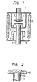
- Fig. 1 shows the structure of a vacuum switch tube, which includes a vacuum insulating container 1, end plates 2 and 3 closing opposite ends of the container 1, and a pair of electrodes 4 and 5 disposed in the container 1 facing each other and mounted on ends of respective electrode rods 6 and 7.
- the electrode rod 7 is connected through a bellows 8 to the end plate 3 such that it is movable axially with respect to the electrode rod 6 while an air-tight seal of the container 1 is maintained.
- shields 9 and 10 are covered by shields 9 and 10, respectively.
- Fig. 2 shows the structure of the electrode 4 or 5 in detail.
- a rear surface of the electrode 5 is welded to the electrode rod 7 by means of welding material 51.
- the electrodes 4 and 5 are formed of the contact material according to the present invention.
- Fig. 3 is a 100 ⁇ magnified photograph showing the crystal grain structure of the conventional Cu-Co alloy contact material for comparison purposes.
- This contact material is obtained by mixing 80 wt% Cu powder and 20 wt% Co powder, and shaping and sintering the mixture.
- Fig. 4 is a 100 ⁇ magnified photograph showing the crystal grain structure of a preferred embodiment of a contact material the present invention, which is a Cu-Co-Ta alloy contact material.
- the Cu-Co-Ta contact material is prepared by mixing 73 wt% Cu powder, 20 wt% Co powder and 7 wt% Ta powder, and then shaping and sintering the mixture. The sintering is performed under conditions for which portions of the Co and Ta react with each other to form Co2Ta. It will be clear from Fig. 4 that in the alloy of the invention Co, Ta, Co2Ta, etc. are uniformly and finely dispersed in the Cu.
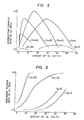
- Fig. 5 is a graph showing the relationship of the interrupting capacity of the inventive Cu-Co-Ta contact material to the amount of Ta with the amount of Co as a parameter in which the interrupting capacity, plotted on the ordinate, is shown as a ratio to the interrupting capacity of the conventional Cu-Co (20 wt% Co) contact material.
- the amount of Ta is plotted on the abscissa.
- solid lines show values having substantially no variation and dotted lines show values having variations.
- the reason why the conventional Cu-Co binary alloy exhibits a good interrupting capacity when Co is present in an amount of 20 wt% and the interrupting capacity decreases when the amount of Co is increased is that Cu, which has a high electrical conductivity, is used to provide the interrupting performance and Co is used to provide properties other than the interrupting performance such as breakdown voltage.
- the alloy of the preferred embodiment of the present invention is prepared by a conventional sintering process, the sintering operation becomes difficult when the total amount of Co and Ta exceeds 60 wt%, which may affect te interrupting performance of the contact alloy adversely. Therefore, the total amount of Co and Ta is set at 60wt% or less. On the contrary, the effect of the coexistence of Co and Ta on the interrupting performance is very small when the total amount thereof is 10 wt% or less.
- Fig. 6 shows the relation between the breakdown voltage and the amount of Ta of the ternary alloy with the amount of Co being set at 0, 5, 20 and 50 wt% as a parameter. On the ordinate is plotted the ratio of the breakdown voltage to that of the conventional Cu-Co alloy, and on the abscissa, the amount of Ta. In Fig. 6, solid lines and dotted lines show values having no variation and values having variation, respectively.
- the breakdown voltage of the ternary alloy is much improved compared with the conventional binary alloy.
- the inventive ternary alloy containing even a small amount of Ta provides a sufficient breakdown voltage performance without sacrificing the interrupting performance.
- the desired interrupting performance is substantially lost.
- the amount of Co should be 5 wt% or more. Further, the total amount of Co and Ta should be 10 wt% or more in view of the breakdown performance.
- the intermetallic compound of Co and Ta i.e., Co2Ta
- Co2Ta the intermetallic compound of Co and Ta
- a contact alloy containing Cu, Co and Ta dispersed in Cu without forming Co2Ta (which can be achieved by using a lower sintering temperature) has substantially the same properties as the alloy containing the intermetallic compound Co2Ta, and exhibits a substantially higher interrupting performance than the conventional Cu-Co alloy.
- Co and Ta which are initially finely dispersed in Cu, react with each other during arc generation. It has been found, however, that the Cu-Co-Ta ternary alloy containing an intermetallic compound of Co and Ta exhibits a higher interrupting performance than the Cu-Co-Ta ternary alloy containing no intermetallic compound.
- the inventive ternary alloy has been described as being prepared by mixing powders of these elements, and shaping and sintering the mixture, the alloy may be manufactured by a melt molding process with substantially the same effects as these obtainable by the sintering process.
- Co in the alloy may be replaced at least partially by Fe with substantially the same effects as the Cu-Co-Ta alloy. This may be for the reason that Fe together with Ta forms an intermetallic compound Fe2Ta, similar to the case of Co, which may affect the interrupting performance advantageously.
- the Cu-Co-Ta ternary alloy or Cu-Fe-Ta ternary alloy further contains at least one of Ti, Zr and Am in an amount of 5 wt% or less, a more favorable interrupting performance can be obtained.
- Ti, Zr and/or Al in the ternary alloy may form a component or components which are effective in improving the interrupting performance.
- the amount of the additive exceeds 5 wt%, the reaction of it with the Cu matrix becomes excessive, providing a substantially reduced electrical conductivity, and hence causing the interrupting performance as well as the contact resistance to be degraded.
- a contact material for use in a low breaking capacity vacuum circuit interrupter which material contains, in addition to the three elements, at least one low melting point metal selected from the group consisting of Bi, Te, Sb, Tl, Pb, Se, Ce and Ca, and alloys thereof, an intermetallic compound thereof and an oxide thereof in an amount of 20 wt% or less is effective in improving the interrupting performance and the breakdown performance as in the case of the above-described embodiment. If the amount of the additive exceeds 20 wt%, the interrupting performance is considerably degraded. It should be noted that if Ce or Ca is used as the low melting point metal, other properties of the contact are slightly degraded.
Landscapes
- Chemical & Material Sciences (AREA)
- Engineering & Computer Science (AREA)
- Materials Engineering (AREA)
- Mechanical Engineering (AREA)
- Metallurgy (AREA)
- Organic Chemistry (AREA)
- High-Tension Arc-Extinguishing Switches Without Spraying Means (AREA)
- Contacts (AREA)
Description
- This invention relates to a contact material for use in a vacuum circuit interrupter and to a contact member of such material, to a vacuum circuit interrupter and to the use of such contact material.
- DE-A-2 034 473 discloses a contact material for a vacuum circuit interrupter, comprising: a first component material of copper; a second component material of tantalum; and a third component material containing at least one of cobalt and iron.
- This document specifies that wetting agents (Fe/Co) should be present in small amounts, and further indicates that increasing the quantity of wetting agent would have adverse effects on the electrical resistance.
- Other contact materials are known from DE-B-2 240 493 and from DE-B-25 35 184, which discloses contact materials for vacuum switches having a powder mixture of Vanadium and copper or chromium and cooper, in which iron, cobalt or nickel powder is added for increasing the sintering activity.
- Vacuum circuit interrupters have been widely used because they are largely maintenance free, pollution free, provide superior interrupting performance, etc. With such interrupters, a large interrupting capacity and a high breakdown voltage are required. The ability to meet these requirements depends largely on the the type of contact material employed.
- Desirable properties of the contact material used for vacuum circuit interrupters include a large interrupting capacity, high breakdown voltage, small contact resistance, low melt bonding, small contact erosion, small chopping current, good reproducibility, high mechanical strength, etc.
- It is very difficult to provide a material which simultaneously satisfies all of these properties, and practical materials satisfy only specific properties necessary for a specific application, sacrificing other properties to some extent.
- U.S. Patent No. 3,379,846 discloses a contact material which is prepared by melt-diffusing a reactive metal such as Zr ou Ti and a high purity metal such as Co. Ag or Au into a sintered refractory metal such as W, Mo, Re, Nb or Ta. U.S. Patent No. 3,859,089 discloses similar materials.
- Copper-bismuth (Cu-Bi), copper-cobalt (Cu-Co), copper-chromium (Cu-Cr), copper-cobalt-bismuth (Cu-Co-Bi), copper-chromium-bismuth (Cu-Cr-Bi) and copper-beryllium (Co-Be), etc. have been used widely as contact materials in view of total performance. Cu-Bi is a non-solid solution of copper which exhibits a high electric conductivity. The amount of bismuth, which is a low-melting point metal and which forms substantially no solid solution with copper, is equal to or larger than a solid solution limit thereof. Although this combination exhibits a good interrupting performance and an anti-melting adhesion capability, the breakdown voltage thereof is very low.
- Specifically, because copper has a high melting point and bismuth is subjected to evaporation and scattering at times of connecting or interrupting a large current and in high voltage applications when contacts are in the open state, the breakdown voltage is low, leading to a degradation of current interrupting performance over time.
- U.S. Patent No. 4,302,514 discloses a contact material composed of copper in which at least one of Cr, Fe and Co is uniformly dispersed with the particle size of the latter being in a range of 80 to 300 µm or in a range of 30 µm or smaller. However, when this material is used to form contacts, the material tends to evaporate at high temperatures in the vacuum container and hence to be deposited on the walls of metal shields and insulating members, resulting in a reduction of the breakdown voltage of the interrupter. Therefore, materials of this kind make the interrupting current large, and thus such materials are not suitable to form contacts of an interrupter for which a high breakdown voltage performance is required. Further, if the amount of copper thereof is larger than a certain value and if the particle size of the dispersed metal is appropriately selected, the interrupting performance is also superior, and therefore such materials have frequently been used for high-voltage, large-current interrupters. However, the anti-melt bonding performance thereof is relatively poor.
- Cu-Co-Bi, Cu-Cr-Bi, etc. have intermediate properties between the above mentioned binary combinations. That is, both of these ternary combinations exhibit relatively superior breakdown performance and interrupting performance and further exhibit superior anti-melt bonding properties due to the presence of Bi. Therefore, such ternary combinations have been used widely. However, since they contain a low melting point metal, the maximum current and voltage which can be applied thereto are necessarily limited.
- However, none of the above-discussed materials is fully satisfactory to meet recent demands for higher performance. Because the performance requirements for interrupters could hitherto not be met by selection of contact material, it has been usual to select the configuration of the contact and/or specially design current passages in the contact portion so that a specific magnetic field is generated therearound by which a large current arc is forcibly driven to thus improve the interrupting performance to some extent. The latter approach, however, is still insufficient to meet increasing requirements of higher voltage and large current handling capability, and thus superior contact materials are still a pressing need.
- The present invention was made in view of the above mentioned defects of the conventional contact materials.
- An object of the present invention is to provide a contact material for use in a vacuum circuit interrupter which has a superior large current interrupting performance and high breakdown voltage performance.
- In order to find contact materials which exhibit higher interrupting current and higher breakdown voltage performances than those of the conventional materials, the inventors prepared contact materials each containing copper and an additive of various metal alloys and/or intermetallic compounds and incorporated them into vacuum switch tubes. Various experiments have been conducted by the inventors on the vacuum switch tubes to evaluate these materials.
- As a result, it has been discovered that for materials containing copper and an additive of Co or Fe, which have been known as providing high vacuum breakdown voltage performance, the breakdown voltage performance is further improved by increasing the amount of Co or Fe. However, the electrical conductivity of the material is remarkably lowered with an increase of Co or Fe, and thus the interrupting performance is lowered. Therefore, for a material containing Cu and Co or Fe, the amount of Co or Fe should be 20 to 30 wt% or less when the interrupting performance is important, resulting in a degraded breakdown voltage.
- As mentioned, a primary object of the invention is to provide a material with which the interrupting performance as well as the breakdown voltage performance is improved. It has been found that the above object can be achieved by a contact material containing a first component of Cu, a second component of Ta, and a third component of at least one of Co and Fe, with the second component being present in an amount of 5 to 30 wt% and the third component being present in an amount of 5 to 30 wt%.
- For a better understanding of the invention, and to show how the same may be carried into effect, reference will now be made, by way of example, to the accompanying drawings, in which:
- Fig. 1 is a cross-sectional view showing a structure of a typical vacuum switch tube;
- Fig. 2 shows an enlarged cross-sectional view of an electrode portion of the tube in Fig. 1;
- Fig. 3 is a 100X magnified photograph showing the crystal grain structure of a conventional Cu-Co (20 wt% Co) contact alloy prepared by sintering;
- Fig. 4 is a 100X magnified photograph showing the crystal grain structure of a preferred embodiment of contact material of the invention which contains 73 wt% Cu, 20 wt% Co, and 7 wt% Ta, and is prepared by sintering at a relatively high temperature;
- Fig. 5 is a characteristic curve showing the interrupting capacity of the contact material of Fig. 4 with the interrupting performance is important, resulting in a degraded breakdown voltage, the amout of Co being varied between 0, 5, 20, 30, 40 and 50 wt% as a parameter, and
- Fig. 6 is a characteristic curve showing the breakdown voltage of the contact material of Fig. 4 with the amount of Co being varied between 0, 5, 20, 30, 40 and 50 wt% as a parameter.
- Fig. 1 shows the structure of a vacuum switch tube, which includes a vacuum insulating container 1,
end plates 2 and 3 closing opposite ends of the container 1, and a pair ofelectrodes 4 and 5 disposed in the container 1 facing each other and mounted on ends ofrespective electrode rods 6 and 7. Theelectrode rod 7 is connected through a bellows 8 to the end plate 3 such that it is movable axially with respect to the electrode rod 6 while an air-tight seal of the container 1 is maintained. In order to prevent an inner wall surface of the container 1 and an outer surface of the bellows 8 from being polluted with metal vapor produced by arcing, etc., they are covered byshields 9 and 10, respectively. - Fig. 2 shows the structure of the
electrode 4 or 5 in detail. A rear surface of theelectrode 5 is welded to theelectrode rod 7 by means ofwelding material 51. Theelectrodes 4 and 5 are formed of the contact material according to the present invention. - Fig. 3 is a 100 × magnified photograph showing the crystal grain structure of the conventional Cu-Co alloy contact material for comparison purposes. This contact material is obtained by mixing 80 wt% Cu powder and 20 wt% Co powder, and shaping and sintering the mixture.
- Fig. 4 is a 100 × magnified photograph showing the crystal grain structure of a preferred embodiment of a contact material the present invention, which is a Cu-Co-Ta alloy contact material. The Cu-Co-Ta contact material is prepared by mixing 73 wt% Cu powder, 20 wt% Co powder and 7 wt% Ta powder, and then shaping and sintering the mixture. The sintering is performed under conditions for which portions of the Co and Ta react with each other to form Co₂Ta. It will be clear from Fig. 4 that in the alloy of the invention Co, Ta, Co₂Ta, etc. are uniformly and finely dispersed in the Cu.
- The properties of this contact material will be described with reference to various experiments. In a comparison example, a Cu-Co alloy containing Cu-Co was employed. Fig. 5 is a graph showing the relationship of the interrupting capacity of the inventive Cu-Co-Ta contact material to the amount of Ta with the amount of Co as a parameter in which the interrupting capacity, plotted on the ordinate, is shown as a ratio to the interrupting capacity of the conventional Cu-Co (20 wt% Co) contact material. The amount of Ta is plotted on the abscissa. Further, in Fig. 5, solid lines show values having substantially no variation and dotted lines show values having variations.
- From Fig. 5, it is clear that even when the amount of Co is set at 0, i.e., for the case of a Cu-Ta binary alloy, the inventive contact material in a certain range of composition ratio exhibits an interrupting capacity above that of the conventional Cu-Co alloy. However, the difference therebetween is not so large. In any case, it is desirable to set the amount of Ta at 60 wt% or less. When Co is added, i.e., Co and Ta are combined with Cu, a remarkable increase of the interrupting capacity is observed. Particularly, with 20 wt% Co and 15 wt% Ta, the interrupting capacity is remarkably high, about twice that of the conventional Cu-Co (20 wt% Co) alloy. With different amounts of Co, i.e., 5, 10, 20, 30, 40 and 50 wt%, there are peak values of interrupting capacity, indicating that there are optimum values of the ratio of Co and Ta.
- The reason why the conventional Cu-Co binary alloy exhibits a good interrupting capacity when Co is present in an amount of 20 wt% and the interrupting capacity decreases when the amount of Co is increased is that Cu, which has a high electrical conductivity, is used to provide the interrupting performance and Co is used to provide properties other than the interrupting performance such as breakdown voltage.
- When Co and Ta are both present, these two elements react on each other in a complicated manner to remarkably improve the interrupting property of the ternary alloy, even though the conductivity of the ternary alloy is lower than that of the conventional binary alloy. This synergistic effect may occur for the reason that the superior interrupting performance of the Cu-Co-Ta ternary alloy is not obtained by the electrical and thermal conductivities of Cu.
- It should be note that when the total amount of Co and Ta of the present ternary alloy is increased beyond a certain value, the interrupting performance will be lowered. This may be for reasons that, setting aside the effect obtainable by the presence of both Co and Ta, effects of a relatively preduced amount of Cu may appear. That is, the electrical and thermal conductivities of the contact alloy may be lowered due to the reduced amount of Cu, which leads to a difficulty of quick dissipation of thermal energy due to arcs, resulting in a lowered interrupting performance. Further, since the alloy of the preferred embodiment of the present invention is prepared by a conventional sintering process, the sintering operation becomes difficult when the total amount of Co and Ta exceeds 60 wt%, which may affect te interrupting performance of the contact alloy adversely. Therefore, the total amount of Co and Ta is set at 60wt% or less. On the contrary, the effect of the coexistence of Co and Ta on the interrupting performance is very small when the total amount thereof is 10 wt% or less.
- Fig. 6 shows the relation between the breakdown voltage and the amount of Ta of the ternary alloy with the amount of Co being set at 0, 5, 20 and 50 wt% as a parameter. On the ordinate is plotted the ratio of the breakdown voltage to that of the conventional Cu-Co alloy, and on the abscissa, the amount of Ta. In Fig. 6, solid lines and dotted lines show values having no variation and values having variation, respectively.
- As is clear from Fig. 6, the breakdown voltage of the ternary alloy is much improved compared with the conventional binary alloy. For example, when the amount of Co is set at 20 wt%, the inventive ternary alloy containing even a small amount of Ta provides a sufficient breakdown voltage performance without sacrificing the interrupting performance. In comparison with the conventional Cu-Co binary alloy containing 50 wt% Co or more, the desired interrupting performance is substantially lost.
- On the other hand, if the amount of Co is small, while a sufficient breakdown voltage performance is expected, it is necessary to increase the amount of Ta. Thus the amount of Co should be 5 wt% or more. Further, the total amount of Co and Ta should be 10 wt% or more in view of the breakdown performance.
- In view of the total performance of the ternary alloy, it is clear from Figs. 5 and 6 that when the amounts of Co and Ta are selected in
ranges 5 to 30 wt% and 5 to 30 wt%, respectively, both the interrupting and breakdown performance are most effectively improved. - It has been found from other measurements of contact resistance of the present ternary alloy contact that the contact resistance becomes a minimum and is stable when the total amount of Co and Ta is 40 wt% or less.
- In experiments the results of which are shown in Figs. 5 and 6, the intermetallic compound of Co and Ta, i.e., Co₂Ta, is formed and Co, Ta and Co₂Ta are uniformly and finely dispersed in Cu. However, a contact alloy containing Cu, Co and Ta dispersed in Cu without forming Co₂Ta (which can be achieved by using a lower sintering temperature) has substantially the same properties as the alloy containing the intermetallic compound Co₂Ta, and exhibits a substantially higher interrupting performance than the conventional Cu-Co alloy. This may be for the reason that Co and Ta, which are initially finely dispersed in Cu, react with each other during arc generation. It has been found, however, that the Cu-Co-Ta ternary alloy containing an intermetallic compound of Co and Ta exhibits a higher interrupting performance than the Cu-Co-Ta ternary alloy containing no intermetallic compound.
- Although the inventive ternary alloy has been described as being prepared by mixing powders of these elements, and shaping and sintering the mixture, the alloy may be manufactured by a melt molding process with substantially the same effects as these obtainable by the sintering process. Further, although not shown, Co in the alloy may be replaced at least partially by Fe with substantially the same effects as the Cu-Co-Ta alloy. This may be for the reason that Fe together with Ta forms an intermetallic compound Fe₂Ta, similar to the case of Co, which may affect the interrupting performance advantageously.
- It has been found that if the Cu-Co-Ta ternary alloy or Cu-Fe-Ta ternary alloy further contains at least one of Ti, Zr and Am in an amount of 5 wt% or less, a more favorable interrupting performance can be obtained. In this case, Ti, Zr and/or Al in the ternary alloy may form a component or components which are effective in improving the interrupting performance. When the amount of the additive exceeds 5 wt%, the reaction of it with the Cu matrix becomes excessive, providing a substantially reduced electrical conductivity, and hence causing the interrupting performance as well as the contact resistance to be degraded.
- Further, it has been found that a contact material for use in a low breaking capacity vacuum circuit interrupter, which material contains, in addition to the three elements, at least one low melting point metal selected from the group consisting of Bi, Te, Sb, Tl, Pb, Se, Ce and Ca, and alloys thereof, an intermetallic compound thereof and an oxide thereof in an amount of 20 wt% or less is effective in improving the interrupting performance and the breakdown performance as in the case of the above-described embodiment. If the amount of the additive exceeds 20 wt%, the interrupting performance is considerably degraded. It should be noted that if Ce or Ca is used as the low melting point metal, other properties of the contact are slightly degraded.
Claims (7)
Applications Claiming Priority (2)
| Application Number | Priority Date | Filing Date | Title |
|---|---|---|---|
| JP58088428A JPS59214123A (en) | 1983-05-18 | 1983-05-18 | Contact material for vacuum breaker |
| JP88428/83 | 1983-05-18 |
Publications (3)
| Publication Number | Publication Date |
|---|---|
| EP0126347A1 EP0126347A1 (en) | 1984-11-28 |
| EP0126347B1 EP0126347B1 (en) | 1986-08-27 |
| EP0126347B2 true EP0126347B2 (en) | 1991-04-24 |
Family
ID=13942510
Family Applications (1)
| Application Number | Title | Priority Date | Filing Date |
|---|---|---|---|
| EP84104949A Expired EP0126347B2 (en) | 1983-05-18 | 1984-05-03 | Contact material for vacuum circuit interrupter, contact member of such material, a vacuum circuit interrupter and the use of such material |
Country Status (4)
| Country | Link |
|---|---|
| US (1) | US4540861A (en) |
| EP (1) | EP0126347B2 (en) |
| JP (1) | JPS59214123A (en) |
| DE (1) | DE3460548D1 (en) |
Families Citing this family (4)
| Publication number | Priority date | Publication date | Assignee | Title |
|---|---|---|---|---|
| JPS60172117A (en) * | 1984-02-17 | 1985-09-05 | 三菱電機株式会社 | Contact for vacuum breaker |
| KR900001613B1 (en) * | 1986-01-10 | 1990-03-17 | 미쯔비시 덴끼 가부시기가이샤 | Contact material for vacuum circuit braker |
| JPS6481130A (en) * | 1987-09-21 | 1989-03-27 | Omron Tateisi Electronics Co | Electrical contact |
| CN113684393B (en) * | 2020-05-22 | 2022-06-17 | 信承瑞技术有限公司 | Preparation process of high-strength high-conductivity copper-selenium alloy contact wire |
Family Cites Families (8)
| Publication number | Priority date | Publication date | Assignee | Title |
|---|---|---|---|---|
| GB1079013A (en) | 1964-04-21 | 1967-08-09 | English Electric Co Ltd | Improvements in or relating to contacts and electrodes |
| GB1194674A (en) * | 1966-05-27 | 1970-06-10 | English Electric Co Ltd | Vacuum Type Electric Circuit Interrupting Devices |
| US3592987A (en) * | 1968-03-19 | 1971-07-13 | Westinghouse Electric Corp | Gettering arrangements for vacuum-type circuit interrupters comprising fibers of gettering material embedded in a matrix of material of good conductivity |
| US3859089A (en) | 1968-05-20 | 1975-01-07 | Minnesota Mining & Mfg | Multiple copy electrophotographic reproduction process |
| US3612795A (en) * | 1969-01-09 | 1971-10-12 | Westinghouse Electric Corp | Shielding arrangements for vacuum-type circuit interrupters of the two-contact type |
| JPS598015B2 (en) | 1978-05-31 | 1984-02-22 | 三菱電機株式会社 | Vacuum shield contact |
| NL7905720A (en) * | 1979-07-24 | 1981-01-27 | Hazemeijer Bv | METHOD FOR IMPROVING SWITCH CONTACTS, IN PARTICULAR FOR VACUUM SWITCHES. |
| DE3136139A1 (en) * | 1981-09-11 | 1983-03-31 | Siemens AG, 1000 Berlin und 8000 München | CONTACT BOLT FOR VACUUM CIRCUIT BREAKER |
-
1983
- 1983-05-18 JP JP58088428A patent/JPS59214123A/en active Granted
-
1984
- 1984-04-12 US US06/599,359 patent/US4540861A/en not_active Expired - Lifetime
- 1984-05-03 DE DE8484104949T patent/DE3460548D1/en not_active Expired
- 1984-05-03 EP EP84104949A patent/EP0126347B2/en not_active Expired
Also Published As
| Publication number | Publication date |
|---|---|
| EP0126347B1 (en) | 1986-08-27 |
| EP0126347A1 (en) | 1984-11-28 |
| US4540861A (en) | 1985-09-10 |
| JPS6340004B2 (en) | 1988-08-09 |
| JPS59214123A (en) | 1984-12-04 |
| DE3460548D1 (en) | 1986-10-02 |
Similar Documents
| Publication | Publication Date | Title |
|---|---|---|
| CA1327131C (en) | Electrical contacts for vacuum interrupter devices | |
| EP0083200B1 (en) | Electrode composition for vacuum switch | |
| EP0110176B1 (en) | Contact material for vacuum circuit breaker | |
| EP0109088B1 (en) | Contact material for vacuum circuit breaker | |
| EP0172912B1 (en) | Contact material for vacuum breaker | |
| EP0126347B2 (en) | Contact material for vacuum circuit interrupter, contact member of such material, a vacuum circuit interrupter and the use of such material | |
| US4424429A (en) | Contactor for vacuum type circuit interrupter | |
| JPH10255603A (en) | Contact material for vacuum valve | |
| JPS6336090B2 (en) | ||
| EP0178796B1 (en) | Manufacture of vacuum interrupter contacts | |
| JPS6336089B2 (en) | ||
| JPH0133011B2 (en) | ||
| JPS59201334A (en) | Contact material for vacuum breaker | |
| JPS6336092B2 (en) | ||
| JPS5914218A (en) | Contact material for vacuum breaker | |
| JPH0449734B2 (en) | ||
| JPH0449733B2 (en) | ||
| JPS59214121A (en) | Contact material for vacuum breaker | |
| JPS60170122A (en) | Contact material for vacuum breaker | |
| JPS59201335A (en) | Contact material for vacuum breaker | |
| JPS59167925A (en) | Contact material for vacuum breaker | |
| JPH0612649B2 (en) | Contact material for vacuum circuit breaker | |
| JPS59201336A (en) | Contact material for vacuum breaker | |
| JPH0133012B2 (en) | ||
| JPS61179827A (en) | Contact for material for vacuum preaker |
Legal Events
| Date | Code | Title | Description |
|---|---|---|---|
| PUAI | Public reference made under article 153(3) epc to a published international application that has entered the european phase |
Free format text: ORIGINAL CODE: 0009012 |
|
| AK | Designated contracting states |
Designated state(s): DE FR GB |
|
| 17P | Request for examination filed |
Effective date: 19841127 |
|
| GRAA | (expected) grant |
Free format text: ORIGINAL CODE: 0009210 |
|
| AK | Designated contracting states |
Kind code of ref document: B1 Designated state(s): DE FR GB |
|
| REF | Corresponds to: |
Ref document number: 3460548 Country of ref document: DE Date of ref document: 19861002 |
|
| ET | Fr: translation filed | ||
| PLBI | Opposition filed |
Free format text: ORIGINAL CODE: 0009260 |
|
| 26 | Opposition filed |
Opponent name: DODUCO KG DR. EUGEN DUERRWAECHTER Effective date: 19870526 |
|
| PUAH | Patent maintained in amended form |
Free format text: ORIGINAL CODE: 0009272 |
|
| STAA | Information on the status of an ep patent application or granted ep patent |
Free format text: STATUS: PATENT MAINTAINED AS AMENDED |
|
| 27A | Patent maintained in amended form |
Effective date: 19910424 |
|
| AK | Designated contracting states |
Kind code of ref document: B2 Designated state(s): DE FR GB |
|
| ET3 | Fr: translation filed ** decision concerning opposition | ||
| REG | Reference to a national code |
Ref country code: FR Ref legal event code: D6 |
|
| REG | Reference to a national code |
Ref country code: GB Ref legal event code: IF02 |
|
| PGFP | Annual fee paid to national office [announced via postgrant information from national office to epo] |
Ref country code: GB Payment date: 20020501 Year of fee payment: 19 |
|
| PGFP | Annual fee paid to national office [announced via postgrant information from national office to epo] |
Ref country code: FR Payment date: 20020508 Year of fee payment: 19 Ref country code: DE Payment date: 20020508 Year of fee payment: 19 |
|
| PG25 | Lapsed in a contracting state [announced via postgrant information from national office to epo] |
Ref country code: GB Free format text: LAPSE BECAUSE OF NON-PAYMENT OF DUE FEES Effective date: 20030503 |
|
| PG25 | Lapsed in a contracting state [announced via postgrant information from national office to epo] |
Ref country code: DE Free format text: LAPSE BECAUSE OF NON-PAYMENT OF DUE FEES Effective date: 20031202 |
|
| GBPC | Gb: european patent ceased through non-payment of renewal fee |
Effective date: 20030503 |
|
| PG25 | Lapsed in a contracting state [announced via postgrant information from national office to epo] |
Ref country code: FR Free format text: LAPSE BECAUSE OF NON-PAYMENT OF DUE FEES Effective date: 20040130 |
|
| REG | Reference to a national code |
Ref country code: FR Ref legal event code: ST |