EP0123831A2 - Convertisseur à haute tension, à piège, de porteur de charge compensé, monté sur une plaquette - Google Patents
Convertisseur à haute tension, à piège, de porteur de charge compensé, monté sur une plaquette Download PDFInfo
- Publication number
- EP0123831A2 EP0123831A2 EP84102329A EP84102329A EP0123831A2 EP 0123831 A2 EP0123831 A2 EP 0123831A2 EP 84102329 A EP84102329 A EP 84102329A EP 84102329 A EP84102329 A EP 84102329A EP 0123831 A2 EP0123831 A2 EP 0123831A2
- Authority
- EP
- European Patent Office
- Prior art keywords
- voltage
- circuit
- charge trapping
- charge pump
- charge
- Prior art date
- Legal status (The legal status is an assumption and is not a legal conclusion. Google has not performed a legal analysis and makes no representation as to the accuracy of the status listed.)
- Granted
Links
Images


Classifications
-
- H—ELECTRICITY
- H02—GENERATION; CONVERSION OR DISTRIBUTION OF ELECTRIC POWER
- H02M—APPARATUS FOR CONVERSION BETWEEN AC AND AC, BETWEEN AC AND DC, OR BETWEEN DC AND DC, AND FOR USE WITH MAINS OR SIMILAR POWER SUPPLY SYSTEMS; CONVERSION OF DC OR AC INPUT POWER INTO SURGE OUTPUT POWER; CONTROL OR REGULATION THEREOF
- H02M3/00—Conversion of dc power input into dc power output
- H02M3/02—Conversion of dc power input into dc power output without intermediate conversion into ac
- H02M3/04—Conversion of dc power input into dc power output without intermediate conversion into ac by static converters
- H02M3/06—Conversion of dc power input into dc power output without intermediate conversion into ac by static converters using resistors or capacitors, e.g. potential divider
- H02M3/07—Conversion of dc power input into dc power output without intermediate conversion into ac by static converters using resistors or capacitors, e.g. potential divider using capacitors charged and discharged alternately by semiconductor devices with control electrode, e.g. charge pumps
- H02M3/073—Charge pumps of the Schenkel-type
-
- G—PHYSICS
- G11—INFORMATION STORAGE
- G11C—STATIC STORES
- G11C5/00—Details of stores covered by group G11C11/00
- G11C5/14—Power supply arrangements, e.g. power down, chip selection or deselection, layout of wirings or power grids, or multiple supply levels
- G11C5/145—Applications of charge pumps; Boosted voltage circuits; Clamp circuits therefor
Definitions
- This invention relates to charge pump operated high voltage converters for converting logic level voltage to high voltage, which can be used for supplying electrically alterable high density memory circuits or electrically alterable silicon semiconductor integrated circuit devices.
- the highest voltage attainable at the output of the circuit is limited by the voltage handling capabilities of the semiconductor technology employed. For present day technology, the limitation presented restricts the upper limit of voltages to less than the level needed for the charge transfer operations in floating gate memory devices.
- an output voltage constraint in the prior art is dependent upon the low voltage device characteristics and does not depend upon tunneling path parameters in the memory device. Output voltage control utilizing low voltage device characteristics do not accurately reflect the changing characteristics of the programmable devices because the tunneling path parameters are not involved in the control circuit.
- over voltage conditions are prevented in the prior art by shunting excessive charge to ground through an output limiting circuit. Thus, the charge pump circuit must operate at maximum capacity at all times with more or less of the excess capacity shunted to ground.
- a further object is to provide an improved high voltage charge pump circuit having an improved feedback path incorporating elements that track the tunneling path parameter variation that results from cyclic operation of the memory cells themselves.
- the output voltage is pumped to a level greater than the predetermined level set in the monitor circuit, the voltage at the gates will be decreased due to the combined charge pump control circuit operation and the monitor circuit so that the voltage at the gates will decrease and will prevent further output voltage increases.
- the output voltage is regulated and the charge pump is not overdriven as it was in the prior art circuits.
- the charge pump monitor circuit utilizing feedback from the output power supply compensates for the charge trapping occurring in the memory cells and increases the drive voltage as is necessary to compensate for the degradation in ease of writing and erasing the memory elements.
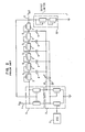
- Each such converter is provided with a logic voltage supply 1 and two phased charging lines 2. The phases are 180° opposite and are applied on the lines 2.
- a series of diodes 3 with intermediate nodes connected to capacitors 4 are shown.
- the alternate capacitors are connected to the alternate phased supply lines 2 as shown.
- Each intermediate node is identified by an alphabetic letter A, B, C...F.
- An output stage 5 shown in the dotted box can filter or smooth or limit the final output voltage at terminals 6.
- Figure 1B illustrates the prior art timing chart for the phase control of the lines 2 in Figure lA.
- a simple flip flop driven by an oscillator can be used to provide such a 180° out of phase timing as would be obvious to those of skill in the art.
- Figure 1C illustrates the output of voltage at each node A, B, C, etc., when the charging lines 2 are pulsed as shown in Figure 1B.
- the bootstrapping charge pump is fairly well known in the art.
- the output current will be relatively limited since the output current is the charge stored in the capacitor 4 at node F.
- a smoothing, integrating and limiting circuit in dotted box 5 consisting of a resistance and capacitance is shown schematically in Figure 1A. It will be described in greater detail below with regard to a prior art circuit embodiment.
- the desired output voltage at terminal 6 may be typically a level of 18 to 25 volts for normal electrically alterable memory program and erase cycles.
- FIG. 2 illustrates a typical prior art charge pump circuit along the lines briefly referred to with regard to Figures 1A-1C. Similar numbering is used for the similar elements in Figures 2 an 1A.
- the filtering and smoothing circuit in dotted box 5 of Figure 1A has been replaced by an output limiter in dotted box 10 and by the feedback path from output node 6 to the charge line drivers in dotted box 9.
- the output limiter 10 comprises a pair of series connected FETs designed to conduct once a specified output voltage has been reached.
- the feedback path from node 6 to the line drivers in dotted box 9 serves to operate the line drivers harder and harder as the output voltage demand is increased.
- a flip flop circuit in dotted box 7 is driven by the oscillator 8 to alternate the output on the two phase control lines 2 as will be apparent.
- the output voltage limiter such as that included in the dotted box 10 of Figure 2 is controlled by low voltage devices and their conduction characteristics and does not depend upon tunneling path parameters present in memory cells that would be operated with the output voltage at node 6.
- the output voltage limiter is controlled by low voltage devices and their conduction characteristics and does not depend upon tunneling path parameters present in memory cells that would be operated with the output voltage at node 6.
- the memory cells suffer degredation due to the well known charge trapping effect, it would be desirable to reduce the limiting effect of circuit 10.
- the over voltage limit is simply a shunt to ground in the circuit included in dotted box 10.
- the charge pump circuit itself must operate at maximum capacity at all times. This limits the available power at output node 6 since the input supplied is only the logic level voltage and current on line 1.
- the voltage monitor circuit in dotted box 9 does not account for parameter variations in the memory cells due to process tolerances and they are not compensated for in the voltage converter circuits. Therefore, a mismatch between the characteristics of the monitoring circuit and those of the memory cells themselves may exist due to fabrication process tolerance variations which may result in inoperable or only marginally operable products as will be appreciated by those of skill in the art.
- FIG 3 a preferred embodiment of the present invention is shown which overcomes the foregoing problems with the known prior art.
- similar numbering and nomenclature is used to indicate elements of similar function or operation to those as shown in Figures 1 and 2.
- the charge pump portion is similar to that shown in Figure 2 but with several differences.
- high voltage protection elements are incorporated at the diode junctions of the FETs 3. These will be described in greater detail later.
- the output limiter in dotted box 10 of Figure 2 has been eliminated in Figure 3.
- the output voltage is instead brought to the input terminal of an output voltage monitor circuit through a feedback circuit that includes a charge trapping monitoring device 11. Its output is supplied to node 12 which is the input to the voltage monitor circuitry.
- the gates of the line drivers Q1 and Q2 in Figure 3 are driven by the charge pump control circuitry.
- the result of the charge pump control circuitry is that when the output voltage is raised to a level greater than the predetermined level set in the monitor circuit, the voltage at the gates will be decreased thereby preventing further output voltage increases. In this manner, the output voltage is regulated, but the charge pump is not over driven as it was for the circuit in Figure 2.
- Devices Q7 and Q8 form a voltage divider network that establishes a reference voltage at the gate of Q11. As the output voltage on node 6 rises above the turn on threshold of the device 11, the gate of Q10 will begin to rise. Devices Q13, Q14 and Q15 are designed in such a manner that a predetermined voltage drop is established from node 12 to the gate of Q10. Once the gate of Q10 increases above the reference level, the gates of Ql and Q2 will be pulled toward ground. This will clamp the output voltage to a predetermined level that is dependent upon the circuit design of the devices Q13, Q14 and Q15 and the reference voltage and on the characteristics of the DEIS element in the feedback path shown as device 11.
- the characteristics of the DEIS device 11 track the variations in tunneling path parameters in memory cell products that will be driven by the voltage supplied at node 6.
- the device 11 is built using the same process techniques so that parameter variations during the circuit formation process are accurately tracked in device 11 to monitor those that will occur in the memory elements built during the same stage of the same process.
- the charge pump circuit in Figure 3 is used each time a program/erase cycle is performed in a memory cell, not shown. Therefore, as charge trapping occurs and fills in sites in the oxide layer of the memory .cells, they are also filled in the feedback element 11 in its dielectric. The result is that an increasing output voltage as a function of the number of cycles of operation will occur. In turn, this increases the total number of cycles that one can achieve in the electrically alterable memory cells beyond that achievable with a fixed voltage design.
- Device 11 is a dual electron injector structure well known in the art. It has been described by DiMaria et al in an article entitled, “Dual Electron Injector Structure Electrically Alterable Read Only Memory Modeling Studies,” appearing in IEEE Transactions on Electron Devices, Sept. 1981, pgs. 1047-1053.
- the structure of device 11 is shown therein and is well known to those of skill in the art.
- the structure consists of chemically vapor deposited silicon rich first and third layers with an intermediate sandwich layer of silicon dioxide. This entire sandwich is packed between polycrystaline silicon layers which act as contacts to the silicon rich silicon dioxide portions of the sandwich. At moderately high electric fields, the structure will conduct current while for low fields it behaves as a good insulator.
- Figures 4A and 4B show the principles of these devices.
- Figure 4A illustrates the prior art DEIS stack.
- the top layer 16 is connected to a voltage supply 17.
- Layer 16 is polycrystaline silicon.
- Layer 18 is a silicon rich silicon dioxide layer that is chemically vapor deposited as described in the foregoing article.
- Layer 19 is a silicon dioxide insulator layer grown to the same thickness and parameters as that used in a memory cell product on the same chip.
- Layer 20 is the same as layer 18 and layer 21 is the same as layer 16.
- the FET diodes in Figure 3 designated with numeral 3 have their source and drain contacts protected from higher voltages by use of protect gate layers.
- the breakdown voltage between the drain and the source will be about 12 volts for an enhancement mode device and about 14 volts in a depletion mode device with the gate to source voltage set at O.
- the 12 and 14 volt levels are simply insufficient to program/erase most electrically alterable FET memory devices.
- Figure 5B illustrates a typical FET with the oxide layers removed for clarity which incorporates a protect gate around the boundaries of the drain diffusion in the substrate. This is a conductive layer that also partially overlies the control gate but is insulated therefrom by an oxide layer. A similar structure may be used between the control gate and around the terminations of the source diffusion. Typically, protection at the drain is sufficient.
- Figure 5C shows an electrical schematic illustrating the protection gate as PG and shows how the breakdown voltage increases from approximately 12 volts to a higher level in the small accompanying voltage plot.
- a protection voltage is applied to the protect gate that prevents drain to source or drain to substrate breakdown in approximately linear fashion as shown. This technique allows the devices to be driven to voltages well above those at which normal breakdown occurs. Voltages in excess of 22 to 25 volts may be sustained in this manner without an unnecessary drain on the charge pump since the protect gate voltage is effectively only a capacitive load of small proportion.
- the high voltage converter described in the preferred embodiment hereof offers unique features for electrically alterable on chip memory technology applications as will be appreciated by those of skill in the art.
- the converter shown provides a way of tracking the electron charge trapping tunneling characteristics for a specific chip on which the converter is built. This eliminates a wide design margin that would otherwise be necessary in order to accommodate for the entire process range. It also adjusts for the electron trapping and causes a voltage adjustment to occur with further usage that helps offset the negative effects of charge trapping in the memory devices.
Landscapes
- Engineering & Computer Science (AREA)
- Power Engineering (AREA)
- Read Only Memory (AREA)
- Semiconductor Integrated Circuits (AREA)
- Metal-Oxide And Bipolar Metal-Oxide Semiconductor Integrated Circuits (AREA)
- Non-Volatile Memory (AREA)
Applications Claiming Priority (2)
| Application Number | Priority Date | Filing Date | Title |
|---|---|---|---|
| US06/481,682 US4481566A (en) | 1983-04-04 | 1983-04-04 | On chip charge trap compensated high voltage converter |
| US481682 | 1995-06-07 |
Publications (3)
| Publication Number | Publication Date |
|---|---|
| EP0123831A2 true EP0123831A2 (fr) | 1984-11-07 |
| EP0123831A3 EP0123831A3 (en) | 1986-02-05 |
| EP0123831B1 EP0123831B1 (fr) | 1989-08-09 |
Family
ID=23912947
Family Applications (1)
| Application Number | Title | Priority Date | Filing Date |
|---|---|---|---|
| EP84102329A Expired EP0123831B1 (fr) | 1983-04-04 | 1984-03-05 | Convertisseur à haute tension, à piège, de porteur de charge compensé, monté sur une plaquette |
Country Status (4)
| Country | Link |
|---|---|
| US (1) | US4481566A (fr) |
| EP (1) | EP0123831B1 (fr) |
| JP (1) | JPS59186200A (fr) |
| DE (1) | DE3479362D1 (fr) |
Cited By (3)
| Publication number | Priority date | Publication date | Assignee | Title |
|---|---|---|---|---|
| EP0328191A1 (fr) * | 1988-02-08 | 1989-08-16 | Koninklijke Philips Electronics N.V. | Circuit de mémorisation muni d'une mémoire programmable effaçable, générateur pour engendrer une tension de programmation pour la mémoire, régulateur de tension et régulateur de flancs convenant pour être utilisés dans le générateur et élément de diode |
| EP0581420A1 (fr) * | 1992-06-22 | 1994-02-02 | Advanced Micro Devices, Inc. | Méthode et dispositif pour la réalisation de liaisons d'interconnexion programmables |
| EP0595330A2 (fr) * | 1992-10-28 | 1994-05-04 | Nec Corporation | Circuit pompe de charge |
Families Citing this family (18)
| Publication number | Priority date | Publication date | Assignee | Title |
|---|---|---|---|---|
| FR2580421A1 (fr) * | 1985-04-12 | 1986-10-17 | Eurotechnique Sa | Memoire morte programmable electriquement |
| JPS6340897U (fr) * | 1986-09-03 | 1988-03-17 | ||
| US4752699A (en) * | 1986-12-19 | 1988-06-21 | International Business Machines Corp. | On chip multiple voltage generation using a charge pump and plural feedback sense circuits |
| NL8702734A (nl) * | 1987-11-17 | 1989-06-16 | Philips Nv | Spanningsvermenigvuldigschakeling en gelijkrichtelement. |
| KR920006991A (ko) * | 1990-09-25 | 1992-04-28 | 김광호 | 반도체메모리 장치의 고전압발생회로 |
| US5414669A (en) * | 1993-09-10 | 1995-05-09 | Intel Corporation | Method and apparatus for programming and erasing flash EEPROM memory arrays utilizing a charge pump circuit |
| EP0661795B1 (fr) * | 1993-12-28 | 1997-07-16 | STMicroelectronics S.r.l. | Survolteur, en particulier pour mémoires non-volatiles |
| US5666045A (en) * | 1994-12-09 | 1997-09-09 | Psc Inc. | Laser drive and control systems useful for laser diode protection |
| US5680300A (en) * | 1995-12-22 | 1997-10-21 | Analog Devices, Inc. | Regulated charge pump DC/DC converter |
| US6055186A (en) * | 1998-10-23 | 2000-04-25 | Macronix International Co., Ltd. | Regulated negative voltage supply circuit for floating gate memory devices |
| US6510394B2 (en) * | 2001-02-02 | 2003-01-21 | Texas Instruments Incorporated | Charge pump with switched capacitor feedback |
| US7372318B2 (en) * | 2004-07-26 | 2008-05-13 | Honeywell International Inc. | Precision, low drift, stacked voltage reference |
| US7161409B2 (en) * | 2004-07-26 | 2007-01-09 | Honeywell International Inc. | Precision, low drift, closed loop voltage reference |
| JP2006236511A (ja) * | 2005-02-25 | 2006-09-07 | Toshiba Corp | 半導体集積回路装置 |
| US8350407B2 (en) | 2007-07-13 | 2013-01-08 | Samsung Electronics Co., Ltd. | High voltage power supply apparatus |
| US8274176B2 (en) * | 2007-07-13 | 2012-09-25 | Samsung Electronics Co., Ltd. | Power supply apparatus |
| US8049551B2 (en) * | 2008-06-17 | 2011-11-01 | Monolithic Power Systems, Inc. | Charge pump for switched capacitor circuits with slew-rate control of in-rush current |
| EP2337200B1 (fr) | 2009-12-18 | 2014-04-09 | Nxp B.V. | Sous-étape pour pompe à charge |
Citations (1)
| Publication number | Priority date | Publication date | Assignee | Title |
|---|---|---|---|---|
| GB2058502A (en) * | 1979-08-31 | 1981-04-08 | Xicor Inc | Integrated rise time regulated voltage generator systems |
Family Cites Families (5)
| Publication number | Priority date | Publication date | Assignee | Title |
|---|---|---|---|---|
| JPS5393350A (en) * | 1977-01-27 | 1978-08-16 | Canon Inc | Booster circuit |
| US4281377A (en) * | 1978-06-21 | 1981-07-28 | Lucas Industries Limited | Power supply circuits |
| FR2437734A1 (fr) * | 1978-09-26 | 1980-04-25 | Thomson Csf | Amplificateur a capacites commutees, filtre a capacites commutees et filtre a transfert de charges comportant un tel amplificateur |
| US4302804A (en) * | 1979-09-04 | 1981-11-24 | Burroughs Corporation | DC Voltage multiplier using phase-sequenced CMOS switches |
| US4321661A (en) * | 1980-12-23 | 1982-03-23 | Gte Laboratories Incorporated | Apparatus for charging a capacitor |
-
1983
- 1983-04-04 US US06/481,682 patent/US4481566A/en not_active Expired - Lifetime
-
1984
- 1984-03-05 DE DE8484102329T patent/DE3479362D1/de not_active Expired
- 1984-03-05 EP EP84102329A patent/EP0123831B1/fr not_active Expired
- 1984-03-07 JP JP59042246A patent/JPS59186200A/ja active Granted
Patent Citations (1)
| Publication number | Priority date | Publication date | Assignee | Title |
|---|---|---|---|---|
| GB2058502A (en) * | 1979-08-31 | 1981-04-08 | Xicor Inc | Integrated rise time regulated voltage generator systems |
Non-Patent Citations (1)
| Title |
|---|
| IBM TECHNICAL DISCLOSURE BULLETIN, vol. 24, no. 8, January 1982, pages 4069-4070, New York, US.; H. CHAO: "Gate-protective diode using dual-electron injector structure" * |
Cited By (5)
| Publication number | Priority date | Publication date | Assignee | Title |
|---|---|---|---|---|
| EP0328191A1 (fr) * | 1988-02-08 | 1989-08-16 | Koninklijke Philips Electronics N.V. | Circuit de mémorisation muni d'une mémoire programmable effaçable, générateur pour engendrer une tension de programmation pour la mémoire, régulateur de tension et régulateur de flancs convenant pour être utilisés dans le générateur et élément de diode |
| EP0581420A1 (fr) * | 1992-06-22 | 1994-02-02 | Advanced Micro Devices, Inc. | Méthode et dispositif pour la réalisation de liaisons d'interconnexion programmables |
| EP0595330A2 (fr) * | 1992-10-28 | 1994-05-04 | Nec Corporation | Circuit pompe de charge |
| EP0595330A3 (fr) * | 1992-10-28 | 1994-12-14 | Nippon Electric Co | Circuit pompe de charge. |
| US5436821A (en) * | 1992-10-28 | 1995-07-25 | Nec Corporation | Low-power charge pump circuit and low-power booster method |
Also Published As
| Publication number | Publication date |
|---|---|
| JPS59186200A (ja) | 1984-10-22 |
| US4481566A (en) | 1984-11-06 |
| EP0123831B1 (fr) | 1989-08-09 |
| EP0123831A3 (en) | 1986-02-05 |
| JPS6255238B2 (fr) | 1987-11-18 |
| DE3479362D1 (en) | 1989-09-14 |
Similar Documents
| Publication | Publication Date | Title |
|---|---|---|
| US4481566A (en) | On chip charge trap compensated high voltage converter | |
| US4229667A (en) | Voltage boosting substrate bias generator | |
| EP0485016B1 (fr) | Circuit de pompe à charge intégré à tension de rétropolarisation réduite | |
| US7102422B1 (en) | Semiconductor booster circuit having cascaded MOS transistors | |
| US4321661A (en) | Apparatus for charging a capacitor | |
| US5754476A (en) | Negative charge pump circuit for electrically erasable semiconductor memory devices | |
| US3878450A (en) | Controlled voltage multiplier providing pulse output | |
| EP0144637B1 (fr) | Système de génération de tension pour une mémoire R.A.M. non-volatile | |
| US4326134A (en) | Integrated rise-time regulated voltage generator systems | |
| KR940011637B1 (ko) | 영속성 메모리 회로 | |
| US5158899A (en) | Method of manufacturing input circuit of semiconductor device | |
| JPH01164264A (ja) | 電圧増倍器集積回路と整流器素子 | |
| US6980043B2 (en) | Ferroelectric element and a ferroelectric gate device using the same | |
| JPH0419639B2 (fr) | ||
| EP0195236A2 (fr) | Générateur de polarisation de substrat semi-conducteur | |
| JPH09191640A (ja) | ネガティブ電圧駆動回路 | |
| EP0144636A1 (fr) | Oscillateur programmable avec possibilité de mise hors circuit et adaptation de fréquence | |
| US7126410B2 (en) | Charge pump with charge injection | |
| US3718826A (en) | Fet address decoder | |
| Bhat et al. | Development of a charge pump for sensor biasing in a Serial Powering scheme for the ATLAS pixel detector upgrade | |
| JPH097371A (ja) | 昇圧電圧供給回路 | |
| EP0851562B1 (fr) | Pompe de charge haute tension en particulier pour mémoires EEPROM flash | |
| JPS63209097A (ja) | 半導体不揮発性ram | |
| JPS61269300A (ja) | アナログ記憶回路 | |
| JPS5931893B2 (ja) | 半導体集積回路 |
Legal Events
| Date | Code | Title | Description |
|---|---|---|---|
| PUAI | Public reference made under article 153(3) epc to a published international application that has entered the european phase |
Free format text: ORIGINAL CODE: 0009012 |
|
| AK | Designated contracting states |
Designated state(s): DE FR GB |
|
| 17P | Request for examination filed |
Effective date: 19841123 |
|
| PUAL | Search report despatched |
Free format text: ORIGINAL CODE: 0009013 |
|
| AK | Designated contracting states |
Designated state(s): DE FR GB |
|
| 17Q | First examination report despatched |
Effective date: 19870730 |
|
| GRAA | (expected) grant |
Free format text: ORIGINAL CODE: 0009210 |
|
| AK | Designated contracting states |
Kind code of ref document: B1 Designated state(s): DE FR GB |
|
| REF | Corresponds to: |
Ref document number: 3479362 Country of ref document: DE Date of ref document: 19890914 |
|
| ET | Fr: translation filed | ||
| PLBE | No opposition filed within time limit |
Free format text: ORIGINAL CODE: 0009261 |
|
| STAA | Information on the status of an ep patent application or granted ep patent |
Free format text: STATUS: NO OPPOSITION FILED WITHIN TIME LIMIT |
|
| 26N | No opposition filed | ||
| PGFP | Annual fee paid to national office [announced via postgrant information from national office to epo] |
Ref country code: GB Payment date: 19940215 Year of fee payment: 11 |
|
| PGFP | Annual fee paid to national office [announced via postgrant information from national office to epo] |
Ref country code: FR Payment date: 19940225 Year of fee payment: 11 |
|
| PGFP | Annual fee paid to national office [announced via postgrant information from national office to epo] |
Ref country code: DE Payment date: 19940329 Year of fee payment: 11 |
|
| PG25 | Lapsed in a contracting state [announced via postgrant information from national office to epo] |
Ref country code: GB Effective date: 19950305 |
|
| GBPC | Gb: european patent ceased through non-payment of renewal fee |
Effective date: 19950305 |
|
| PG25 | Lapsed in a contracting state [announced via postgrant information from national office to epo] |
Ref country code: FR Free format text: LAPSE BECAUSE OF NON-PAYMENT OF DUE FEES Effective date: 19951130 |
|
| PG25 | Lapsed in a contracting state [announced via postgrant information from national office to epo] |
Ref country code: DE Effective date: 19951201 |
|
| REG | Reference to a national code |
Ref country code: FR Ref legal event code: ST |