EP0122687B1 - A semiconductor device comprising packing means for protecting parts of the device - Google Patents
A semiconductor device comprising packing means for protecting parts of the device Download PDFInfo
- Publication number
- EP0122687B1 EP0122687B1 EP84300521A EP84300521A EP0122687B1 EP 0122687 B1 EP0122687 B1 EP 0122687B1 EP 84300521 A EP84300521 A EP 84300521A EP 84300521 A EP84300521 A EP 84300521A EP 0122687 B1 EP0122687 B1 EP 0122687B1
- Authority
- EP
- European Patent Office
- Prior art keywords
- semiconductor device
- layers
- accordance
- layer
- metallic
- Prior art date
- Legal status (The legal status is an assumption and is not a legal conclusion. Google has not performed a legal analysis and makes no representation as to the accuracy of the status listed.)
- Expired
Links
- 239000004065 semiconductor Substances 0.000 title claims description 96
- 238000012856 packing Methods 0.000 title description 81
- 239000000463 material Substances 0.000 claims description 45
- 230000003014 reinforcing effect Effects 0.000 claims description 36
- 229920005989 resin Polymers 0.000 claims description 30
- 239000011347 resin Substances 0.000 claims description 30
- 229910052751 metal Inorganic materials 0.000 claims description 13
- 239000002184 metal Substances 0.000 claims description 13
- 239000000835 fiber Substances 0.000 claims description 10
- 229920001187 thermosetting polymer Polymers 0.000 claims description 7
- 239000000919 ceramic Substances 0.000 claims description 6
- 239000011521 glass Substances 0.000 claims description 6
- 229920005992 thermoplastic resin Polymers 0.000 claims description 6
- 239000000123 paper Substances 0.000 claims description 5
- 230000002093 peripheral effect Effects 0.000 claims description 5
- 239000010425 asbestos Substances 0.000 claims description 4
- 230000004927 fusion Effects 0.000 claims description 4
- 239000010445 mica Substances 0.000 claims description 4
- 229910052618 mica group Inorganic materials 0.000 claims description 4
- 229910052895 riebeckite Inorganic materials 0.000 claims description 4
- 239000011365 complex material Substances 0.000 claims description 3
- 239000011261 inert gas Substances 0.000 claims description 2
- XLYOFNOQVPJJNP-UHFFFAOYSA-N water Substances O XLYOFNOQVPJJNP-UHFFFAOYSA-N 0.000 claims description 2
- 239000010410 layer Substances 0.000 description 120
- 238000012360 testing method Methods 0.000 description 34
- 239000003822 epoxy resin Substances 0.000 description 21
- 229920000647 polyepoxide Polymers 0.000 description 21
- 239000011133 lead Substances 0.000 description 20
- 229910052782 aluminium Inorganic materials 0.000 description 12
- XAGFODPZIPBFFR-UHFFFAOYSA-N aluminium Chemical compound [Al] XAGFODPZIPBFFR-UHFFFAOYSA-N 0.000 description 12
- 238000000034 method Methods 0.000 description 12
- 238000007789 sealing Methods 0.000 description 12
- 238000004519 manufacturing process Methods 0.000 description 10
- 239000011888 foil Substances 0.000 description 8
- 230000002285 radioactive effect Effects 0.000 description 7
- XEEYBQQBJWHFJM-UHFFFAOYSA-N Iron Chemical compound [Fe] XEEYBQQBJWHFJM-UHFFFAOYSA-N 0.000 description 6
- 239000004067 bulking agent Substances 0.000 description 6
- -1 polyethylene Polymers 0.000 description 6
- 239000003795 chemical substances by application Substances 0.000 description 5
- 239000000203 mixture Substances 0.000 description 5
- 239000011368 organic material Substances 0.000 description 5
- 229920000728 polyester Polymers 0.000 description 5
- 239000003566 sealing material Substances 0.000 description 5
- 238000001721 transfer moulding Methods 0.000 description 5
- PXHVJJICTQNCMI-UHFFFAOYSA-N Nickel Chemical compound [Ni] PXHVJJICTQNCMI-UHFFFAOYSA-N 0.000 description 4
- 239000003365 glass fiber Substances 0.000 description 4
- PCHJSUWPFVWCPO-UHFFFAOYSA-N gold Chemical compound [Au] PCHJSUWPFVWCPO-UHFFFAOYSA-N 0.000 description 4
- 230000006872 improvement Effects 0.000 description 4
- 238000000465 moulding Methods 0.000 description 4
- RYGMFSIKBFXOCR-UHFFFAOYSA-N Copper Chemical compound [Cu] RYGMFSIKBFXOCR-UHFFFAOYSA-N 0.000 description 3
- 239000004734 Polyphenylene sulfide Substances 0.000 description 3
- VYPSYNLAJGMNEJ-UHFFFAOYSA-N Silicium dioxide Chemical compound O=[Si]=O VYPSYNLAJGMNEJ-UHFFFAOYSA-N 0.000 description 3
- 229910052802 copper Inorganic materials 0.000 description 3
- 239000010949 copper Substances 0.000 description 3
- 230000007797 corrosion Effects 0.000 description 3
- 238000005260 corrosion Methods 0.000 description 3
- 230000003247 decreasing effect Effects 0.000 description 3
- 239000007789 gas Substances 0.000 description 3
- 229910052737 gold Inorganic materials 0.000 description 3
- 239000010931 gold Substances 0.000 description 3
- 229910052742 iron Inorganic materials 0.000 description 3
- 239000012778 molding material Substances 0.000 description 3
- 230000000149 penetrating effect Effects 0.000 description 3
- 229920000069 polyphenylene sulfide Polymers 0.000 description 3
- 230000035939 shock Effects 0.000 description 3
- 229920002050 silicone resin Polymers 0.000 description 3
- 239000010935 stainless steel Substances 0.000 description 3
- 229910001220 stainless steel Inorganic materials 0.000 description 3
- 239000000126 substance Substances 0.000 description 3
- ZSLUVFAKFWKJRC-IGMARMGPSA-N 232Th Chemical compound [232Th] ZSLUVFAKFWKJRC-IGMARMGPSA-N 0.000 description 2
- XKRFYHLGVUSROY-UHFFFAOYSA-N Argon Chemical compound [Ar] XKRFYHLGVUSROY-UHFFFAOYSA-N 0.000 description 2
- VGGSQFUCUMXWEO-UHFFFAOYSA-N Ethene Chemical compound C=C VGGSQFUCUMXWEO-UHFFFAOYSA-N 0.000 description 2
- 239000005977 Ethylene Substances 0.000 description 2
- 239000004640 Melamine resin Substances 0.000 description 2
- 229920000877 Melamine resin Polymers 0.000 description 2
- 239000004696 Poly ether ether ketone Substances 0.000 description 2
- 239000004952 Polyamide Substances 0.000 description 2
- 239000004698 Polyethylene Substances 0.000 description 2
- 239000004642 Polyimide Substances 0.000 description 2
- 239000004743 Polypropylene Substances 0.000 description 2
- 239000004372 Polyvinyl alcohol Substances 0.000 description 2
- 229910052776 Thorium Inorganic materials 0.000 description 2
- RTAQQCXQSZGOHL-UHFFFAOYSA-N Titanium Chemical compound [Ti] RTAQQCXQSZGOHL-UHFFFAOYSA-N 0.000 description 2
- 229910052770 Uranium Inorganic materials 0.000 description 2
- 229910045601 alloy Inorganic materials 0.000 description 2
- 239000000956 alloy Substances 0.000 description 2
- 239000012298 atmosphere Substances 0.000 description 2
- 239000011248 coating agent Substances 0.000 description 2
- 238000000576 coating method Methods 0.000 description 2
- 239000007822 coupling agent Substances 0.000 description 2
- 238000010438 heat treatment Methods 0.000 description 2
- 239000012535 impurity Substances 0.000 description 2
- 229910010272 inorganic material Inorganic materials 0.000 description 2
- 239000011147 inorganic material Substances 0.000 description 2
- 230000010354 integration Effects 0.000 description 2
- 150000002739 metals Chemical class 0.000 description 2
- 238000002156 mixing Methods 0.000 description 2
- 229910052759 nickel Inorganic materials 0.000 description 2
- 239000005011 phenolic resin Substances 0.000 description 2
- 229920002647 polyamide Polymers 0.000 description 2
- 239000004417 polycarbonate Substances 0.000 description 2
- 229920000515 polycarbonate Polymers 0.000 description 2
- 229920002530 polyetherether ketone Polymers 0.000 description 2
- 229920000573 polyethylene Polymers 0.000 description 2
- 229920001721 polyimide Polymers 0.000 description 2
- 229920001155 polypropylene Polymers 0.000 description 2
- 229920005749 polyurethane resin Polymers 0.000 description 2
- 229920002451 polyvinyl alcohol Polymers 0.000 description 2
- 239000004800 polyvinyl chloride Substances 0.000 description 2
- 229920000915 polyvinyl chloride Polymers 0.000 description 2
- 239000002356 single layer Substances 0.000 description 2
- 229920003002 synthetic resin Polymers 0.000 description 2
- 239000000057 synthetic resin Substances 0.000 description 2
- DLYUQMMRRRQYAE-UHFFFAOYSA-N tetraphosphorus decaoxide Chemical compound O1P(O2)(=O)OP3(=O)OP1(=O)OP2(=O)O3 DLYUQMMRRRQYAE-UHFFFAOYSA-N 0.000 description 2
- 239000010936 titanium Substances 0.000 description 2
- 229910052719 titanium Inorganic materials 0.000 description 2
- 229920006337 unsaturated polyester resin Polymers 0.000 description 2
- JFALSRSLKYAFGM-UHFFFAOYSA-N uranium(0) Chemical compound [U] JFALSRSLKYAFGM-UHFFFAOYSA-N 0.000 description 2
- OUPZKGBUJRBPGC-UHFFFAOYSA-N 1,3,5-tris(oxiran-2-ylmethyl)-1,3,5-triazinane-2,4,6-trione Chemical compound O=C1N(CC2OC2)C(=O)N(CC2OC2)C(=O)N1CC1CO1 OUPZKGBUJRBPGC-UHFFFAOYSA-N 0.000 description 1
- KUBDPQJOLOUJRM-UHFFFAOYSA-N 2-(chloromethyl)oxirane;4-[2-(4-hydroxyphenyl)propan-2-yl]phenol Chemical compound ClCC1CO1.C=1C=C(O)C=CC=1C(C)(C)C1=CC=C(O)C=C1 KUBDPQJOLOUJRM-UHFFFAOYSA-N 0.000 description 1
- IJGRMHOSHXDMSA-UHFFFAOYSA-N Atomic nitrogen Chemical compound N#N IJGRMHOSHXDMSA-UHFFFAOYSA-N 0.000 description 1
- 229920001342 Bakelite® Polymers 0.000 description 1
- FYYHWMGAXLPEAU-UHFFFAOYSA-N Magnesium Chemical compound [Mg] FYYHWMGAXLPEAU-UHFFFAOYSA-N 0.000 description 1
- ISWSIDIOOBJBQZ-UHFFFAOYSA-N Phenol Chemical compound OC1=CC=CC=C1 ISWSIDIOOBJBQZ-UHFFFAOYSA-N 0.000 description 1
- 229930182556 Polyacetal Natural products 0.000 description 1
- 239000004962 Polyamide-imide Substances 0.000 description 1
- 239000004721 Polyphenylene oxide Substances 0.000 description 1
- 239000004793 Polystyrene Substances 0.000 description 1
- ATJFFYVFTNAWJD-UHFFFAOYSA-N Tin Chemical compound [Sn] ATJFFYVFTNAWJD-UHFFFAOYSA-N 0.000 description 1
- 229920001807 Urea-formaldehyde Polymers 0.000 description 1
- HCHKCACWOHOZIP-UHFFFAOYSA-N Zinc Chemical compound [Zn] HCHKCACWOHOZIP-UHFFFAOYSA-N 0.000 description 1
- DHKHKXVYLBGOIT-UHFFFAOYSA-N acetaldehyde Diethyl Acetal Natural products CCOC(C)OCC DHKHKXVYLBGOIT-UHFFFAOYSA-N 0.000 description 1
- 125000002777 acetyl group Chemical class [H]C([H])([H])C(*)=O 0.000 description 1
- 239000002253 acid Substances 0.000 description 1
- NIXOWILDQLNWCW-UHFFFAOYSA-N acrylic acid group Chemical group C(C=C)(=O)O NIXOWILDQLNWCW-UHFFFAOYSA-N 0.000 description 1
- 239000000853 adhesive Substances 0.000 description 1
- 230000001070 adhesive effect Effects 0.000 description 1
- AZDRQVAHHNSJOQ-UHFFFAOYSA-N alumane Chemical group [AlH3] AZDRQVAHHNSJOQ-UHFFFAOYSA-N 0.000 description 1
- ARCGXLSVLAOJQL-UHFFFAOYSA-N anhydrous trimellitic acid Natural products OC(=O)C1=CC=C(C(O)=O)C(C(O)=O)=C1 ARCGXLSVLAOJQL-UHFFFAOYSA-N 0.000 description 1
- 229910052787 antimony Inorganic materials 0.000 description 1
- WATWJIUSRGPENY-UHFFFAOYSA-N antimony atom Chemical compound [Sb] WATWJIUSRGPENY-UHFFFAOYSA-N 0.000 description 1
- 229910052786 argon Inorganic materials 0.000 description 1
- 238000005452 bending Methods 0.000 description 1
- 230000005540 biological transmission Effects 0.000 description 1
- 239000003990 capacitor Substances 0.000 description 1
- 229910017052 cobalt Inorganic materials 0.000 description 1
- 239000010941 cobalt Substances 0.000 description 1
- GUTLYIVDDKVIGB-UHFFFAOYSA-N cobalt atom Chemical compound [Co] GUTLYIVDDKVIGB-UHFFFAOYSA-N 0.000 description 1
- GVPFVAHMJGGAJG-UHFFFAOYSA-L cobalt dichloride Chemical compound [Cl-].[Cl-].[Co+2] GVPFVAHMJGGAJG-UHFFFAOYSA-L 0.000 description 1
- 239000003086 colorant Substances 0.000 description 1
- 238000000748 compression moulding Methods 0.000 description 1
- 230000006378 damage Effects 0.000 description 1
- 230000006866 deterioration Effects 0.000 description 1
- 229910001873 dinitrogen Inorganic materials 0.000 description 1
- ZZTCPWRAHWXWCH-UHFFFAOYSA-N diphenylmethanediamine Chemical compound C=1C=CC=CC=1C(N)(N)C1=CC=CC=C1 ZZTCPWRAHWXWCH-UHFFFAOYSA-N 0.000 description 1
- LNEPOXFFQSENCJ-UHFFFAOYSA-N haloperidol Chemical compound C1CC(O)(C=2C=CC(Cl)=CC=2)CCN1CCCC(=O)C1=CC=C(F)C=C1 LNEPOXFFQSENCJ-UHFFFAOYSA-N 0.000 description 1
- 229910000856 hastalloy Inorganic materials 0.000 description 1
- 239000001307 helium Substances 0.000 description 1
- 229910052734 helium Inorganic materials 0.000 description 1
- SWQJXJOGLNCZEY-UHFFFAOYSA-N helium atom Chemical compound [He] SWQJXJOGLNCZEY-UHFFFAOYSA-N 0.000 description 1
- PYGSKMBEVAICCR-UHFFFAOYSA-N hexa-1,5-diene Chemical group C=CCCC=C PYGSKMBEVAICCR-UHFFFAOYSA-N 0.000 description 1
- 229910001026 inconel Inorganic materials 0.000 description 1
- 238000005304 joining Methods 0.000 description 1
- 150000002576 ketones Chemical class 0.000 description 1
- 229910052743 krypton Inorganic materials 0.000 description 1
- DNNSSWSSYDEUBZ-UHFFFAOYSA-N krypton atom Chemical compound [Kr] DNNSSWSSYDEUBZ-UHFFFAOYSA-N 0.000 description 1
- 229910052749 magnesium Inorganic materials 0.000 description 1
- 239000011777 magnesium Substances 0.000 description 1
- 229910052754 neon Inorganic materials 0.000 description 1
- GKAOGPIIYCISHV-UHFFFAOYSA-N neon atom Chemical compound [Ne] GKAOGPIIYCISHV-UHFFFAOYSA-N 0.000 description 1
- 239000004745 nonwoven fabric Substances 0.000 description 1
- 229920003986 novolac Polymers 0.000 description 1
- 229920002492 poly(sulfone) Polymers 0.000 description 1
- 229920002239 polyacrylonitrile Polymers 0.000 description 1
- 229920002312 polyamide-imide Polymers 0.000 description 1
- 229920000570 polyether Polymers 0.000 description 1
- 229920006324 polyoxymethylene Polymers 0.000 description 1
- 229920002223 polystyrene Polymers 0.000 description 1
- 238000003825 pressing Methods 0.000 description 1
- 230000002265 prevention Effects 0.000 description 1
- 238000003672 processing method Methods 0.000 description 1
- 229920006395 saturated elastomer Polymers 0.000 description 1
- 239000000741 silica gel Substances 0.000 description 1
- 229910002027 silica gel Inorganic materials 0.000 description 1
- 239000000377 silicon dioxide Substances 0.000 description 1
- 239000000758 substrate Substances 0.000 description 1
- 239000012756 surface treatment agent Substances 0.000 description 1
- 239000011135 tin Substances 0.000 description 1
- 229910052718 tin Inorganic materials 0.000 description 1
- WFKWXMTUELFFGS-UHFFFAOYSA-N tungsten Chemical compound [W] WFKWXMTUELFFGS-UHFFFAOYSA-N 0.000 description 1
- 229910052721 tungsten Inorganic materials 0.000 description 1
- 239000010937 tungsten Substances 0.000 description 1
- 229920002554 vinyl polymer Polymers 0.000 description 1
- 229910052724 xenon Inorganic materials 0.000 description 1
- FHNFHKCVQCLJFQ-UHFFFAOYSA-N xenon atom Chemical compound [Xe] FHNFHKCVQCLJFQ-UHFFFAOYSA-N 0.000 description 1
- 229910052725 zinc Inorganic materials 0.000 description 1
- 239000011701 zinc Substances 0.000 description 1
Images


Classifications
-
- H—ELECTRICITY
- H01—ELECTRIC ELEMENTS
- H01L—SEMICONDUCTOR DEVICES NOT COVERED BY CLASS H10
- H01L21/00—Processes or apparatus adapted for the manufacture or treatment of semiconductor or solid state devices or of parts thereof
- H01L21/02—Manufacture or treatment of semiconductor devices or of parts thereof
- H01L21/04—Manufacture or treatment of semiconductor devices or of parts thereof the devices having potential barriers, e.g. a PN junction, depletion layer or carrier concentration layer
- H01L21/50—Assembly of semiconductor devices using processes or apparatus not provided for in a single one of the groups H01L21/18 - H01L21/326 or H10D48/04 - H10D48/07 e.g. sealing of a cap to a base of a container
- H01L21/56—Encapsulations, e.g. encapsulation layers, coatings
- H01L21/565—Moulds
-
- H—ELECTRICITY
- H01—ELECTRIC ELEMENTS
- H01L—SEMICONDUCTOR DEVICES NOT COVERED BY CLASS H10
- H01L23/00—Details of semiconductor or other solid state devices
- H01L23/02—Containers; Seals
- H01L23/04—Containers; Seals characterised by the shape of the container or parts, e.g. caps, walls
- H01L23/053—Containers; Seals characterised by the shape of the container or parts, e.g. caps, walls the container being a hollow construction and having an insulating or insulated base as a mounting for the semiconductor body
- H01L23/057—Containers; Seals characterised by the shape of the container or parts, e.g. caps, walls the container being a hollow construction and having an insulating or insulated base as a mounting for the semiconductor body the leads being parallel to the base
-
- H—ELECTRICITY
- H01—ELECTRIC ELEMENTS
- H01L—SEMICONDUCTOR DEVICES NOT COVERED BY CLASS H10
- H01L23/00—Details of semiconductor or other solid state devices
- H01L23/02—Containers; Seals
- H01L23/06—Containers; Seals characterised by the material of the container or its electrical properties
- H01L23/08—Containers; Seals characterised by the material of the container or its electrical properties the material being an electrical insulator, e.g. glass
-
- H—ELECTRICITY
- H01—ELECTRIC ELEMENTS
- H01L—SEMICONDUCTOR DEVICES NOT COVERED BY CLASS H10
- H01L23/00—Details of semiconductor or other solid state devices
- H01L23/12—Mountings, e.g. non-detachable insulating substrates
- H01L23/14—Mountings, e.g. non-detachable insulating substrates characterised by the material or its electrical properties
- H01L23/145—Organic substrates, e.g. plastic
-
- H—ELECTRICITY
- H01—ELECTRIC ELEMENTS
- H01L—SEMICONDUCTOR DEVICES NOT COVERED BY CLASS H10
- H01L23/00—Details of semiconductor or other solid state devices
- H01L23/16—Fillings or auxiliary members in containers or encapsulations, e.g. centering rings
- H01L23/18—Fillings characterised by the material, its physical or chemical properties, or its arrangement within the complete device
- H01L23/20—Fillings characterised by the material, its physical or chemical properties, or its arrangement within the complete device gaseous at the normal operating temperature of the device
-
- H—ELECTRICITY
- H01—ELECTRIC ELEMENTS
- H01L—SEMICONDUCTOR DEVICES NOT COVERED BY CLASS H10
- H01L23/00—Details of semiconductor or other solid state devices
- H01L23/16—Fillings or auxiliary members in containers or encapsulations, e.g. centering rings
- H01L23/18—Fillings characterised by the material, its physical or chemical properties, or its arrangement within the complete device
- H01L23/26—Fillings characterised by the material, its physical or chemical properties, or its arrangement within the complete device including materials for absorbing or reacting with moisture or other undesired substances, e.g. getters
-
- H—ELECTRICITY
- H01—ELECTRIC ELEMENTS
- H01L—SEMICONDUCTOR DEVICES NOT COVERED BY CLASS H10
- H01L23/00—Details of semiconductor or other solid state devices
- H01L23/28—Encapsulations, e.g. encapsulating layers, coatings, e.g. for protection
- H01L23/29—Encapsulations, e.g. encapsulating layers, coatings, e.g. for protection characterised by the material, e.g. carbon
- H01L23/293—Organic, e.g. plastic
-
- H—ELECTRICITY
- H01—ELECTRIC ELEMENTS
- H01L—SEMICONDUCTOR DEVICES NOT COVERED BY CLASS H10
- H01L23/00—Details of semiconductor or other solid state devices
- H01L23/28—Encapsulations, e.g. encapsulating layers, coatings, e.g. for protection
- H01L23/31—Encapsulations, e.g. encapsulating layers, coatings, e.g. for protection characterised by the arrangement or shape
- H01L23/3107—Encapsulations, e.g. encapsulating layers, coatings, e.g. for protection characterised by the arrangement or shape the device being completely enclosed
- H01L23/315—Encapsulations, e.g. encapsulating layers, coatings, e.g. for protection characterised by the arrangement or shape the device being completely enclosed the encapsulation having a cavity
-
- H—ELECTRICITY
- H01—ELECTRIC ELEMENTS
- H01L—SEMICONDUCTOR DEVICES NOT COVERED BY CLASS H10
- H01L24/00—Arrangements for connecting or disconnecting semiconductor or solid-state bodies; Methods or apparatus related thereto
- H01L24/93—Batch processes
- H01L24/95—Batch processes at chip-level, i.e. with connecting carried out on a plurality of singulated devices, i.e. on diced chips
- H01L24/97—Batch processes at chip-level, i.e. with connecting carried out on a plurality of singulated devices, i.e. on diced chips the devices being connected to a common substrate, e.g. interposer, said common substrate being separable into individual assemblies after connecting
-
- H—ELECTRICITY
- H01—ELECTRIC ELEMENTS
- H01L—SEMICONDUCTOR DEVICES NOT COVERED BY CLASS H10
- H01L2224/00—Indexing scheme for arrangements for connecting or disconnecting semiconductor or solid-state bodies and methods related thereto as covered by H01L24/00
- H01L2224/01—Means for bonding being attached to, or being formed on, the surface to be connected, e.g. chip-to-package, die-attach, "first-level" interconnects; Manufacturing methods related thereto
- H01L2224/42—Wire connectors; Manufacturing methods related thereto
- H01L2224/44—Structure, shape, material or disposition of the wire connectors prior to the connecting process
- H01L2224/45—Structure, shape, material or disposition of the wire connectors prior to the connecting process of an individual wire connector
- H01L2224/45001—Core members of the connector
- H01L2224/4501—Shape
- H01L2224/45012—Cross-sectional shape
- H01L2224/45015—Cross-sectional shape being circular
-
- H—ELECTRICITY
- H01—ELECTRIC ELEMENTS
- H01L—SEMICONDUCTOR DEVICES NOT COVERED BY CLASS H10
- H01L2224/00—Indexing scheme for arrangements for connecting or disconnecting semiconductor or solid-state bodies and methods related thereto as covered by H01L24/00
- H01L2224/01—Means for bonding being attached to, or being formed on, the surface to be connected, e.g. chip-to-package, die-attach, "first-level" interconnects; Manufacturing methods related thereto
- H01L2224/42—Wire connectors; Manufacturing methods related thereto
- H01L2224/44—Structure, shape, material or disposition of the wire connectors prior to the connecting process
- H01L2224/45—Structure, shape, material or disposition of the wire connectors prior to the connecting process of an individual wire connector
- H01L2224/45001—Core members of the connector
- H01L2224/45099—Material
- H01L2224/451—Material with a principal constituent of the material being a metal or a metalloid, e.g. boron (B), silicon (Si), germanium (Ge), arsenic (As), antimony (Sb), tellurium (Te) and polonium (Po), and alloys thereof
- H01L2224/45117—Material with a principal constituent of the material being a metal or a metalloid, e.g. boron (B), silicon (Si), germanium (Ge), arsenic (As), antimony (Sb), tellurium (Te) and polonium (Po), and alloys thereof the principal constituent melting at a temperature of greater than or equal to 400°C and less than 950°C
- H01L2224/45124—Aluminium (Al) as principal constituent
-
- H—ELECTRICITY
- H01—ELECTRIC ELEMENTS
- H01L—SEMICONDUCTOR DEVICES NOT COVERED BY CLASS H10
- H01L2224/00—Indexing scheme for arrangements for connecting or disconnecting semiconductor or solid-state bodies and methods related thereto as covered by H01L24/00
- H01L2224/01—Means for bonding being attached to, or being formed on, the surface to be connected, e.g. chip-to-package, die-attach, "first-level" interconnects; Manufacturing methods related thereto
- H01L2224/42—Wire connectors; Manufacturing methods related thereto
- H01L2224/44—Structure, shape, material or disposition of the wire connectors prior to the connecting process
- H01L2224/45—Structure, shape, material or disposition of the wire connectors prior to the connecting process of an individual wire connector
- H01L2224/45001—Core members of the connector
- H01L2224/45099—Material
- H01L2224/451—Material with a principal constituent of the material being a metal or a metalloid, e.g. boron (B), silicon (Si), germanium (Ge), arsenic (As), antimony (Sb), tellurium (Te) and polonium (Po), and alloys thereof
- H01L2224/45138—Material with a principal constituent of the material being a metal or a metalloid, e.g. boron (B), silicon (Si), germanium (Ge), arsenic (As), antimony (Sb), tellurium (Te) and polonium (Po), and alloys thereof the principal constituent melting at a temperature of greater than or equal to 950°C and less than 1550°C
- H01L2224/45144—Gold (Au) as principal constituent
-
- H—ELECTRICITY
- H01—ELECTRIC ELEMENTS
- H01L—SEMICONDUCTOR DEVICES NOT COVERED BY CLASS H10
- H01L2224/00—Indexing scheme for arrangements for connecting or disconnecting semiconductor or solid-state bodies and methods related thereto as covered by H01L24/00
- H01L2224/01—Means for bonding being attached to, or being formed on, the surface to be connected, e.g. chip-to-package, die-attach, "first-level" interconnects; Manufacturing methods related thereto
- H01L2224/42—Wire connectors; Manufacturing methods related thereto
- H01L2224/47—Structure, shape, material or disposition of the wire connectors after the connecting process
- H01L2224/48—Structure, shape, material or disposition of the wire connectors after the connecting process of an individual wire connector
- H01L2224/4805—Shape
- H01L2224/4809—Loop shape
- H01L2224/48091—Arched
-
- H—ELECTRICITY
- H01—ELECTRIC ELEMENTS
- H01L—SEMICONDUCTOR DEVICES NOT COVERED BY CLASS H10
- H01L2224/00—Indexing scheme for arrangements for connecting or disconnecting semiconductor or solid-state bodies and methods related thereto as covered by H01L24/00
- H01L2224/01—Means for bonding being attached to, or being formed on, the surface to be connected, e.g. chip-to-package, die-attach, "first-level" interconnects; Manufacturing methods related thereto
- H01L2224/42—Wire connectors; Manufacturing methods related thereto
- H01L2224/47—Structure, shape, material or disposition of the wire connectors after the connecting process
- H01L2224/48—Structure, shape, material or disposition of the wire connectors after the connecting process of an individual wire connector
- H01L2224/481—Disposition
- H01L2224/48151—Connecting between a semiconductor or solid-state body and an item not being a semiconductor or solid-state body, e.g. chip-to-substrate, chip-to-passive
- H01L2224/48221—Connecting between a semiconductor or solid-state body and an item not being a semiconductor or solid-state body, e.g. chip-to-substrate, chip-to-passive the body and the item being stacked
- H01L2224/48245—Connecting between a semiconductor or solid-state body and an item not being a semiconductor or solid-state body, e.g. chip-to-substrate, chip-to-passive the body and the item being stacked the item being metallic
- H01L2224/48247—Connecting between a semiconductor or solid-state body and an item not being a semiconductor or solid-state body, e.g. chip-to-substrate, chip-to-passive the body and the item being stacked the item being metallic connecting the wire to a bond pad of the item
-
- H—ELECTRICITY
- H01—ELECTRIC ELEMENTS
- H01L—SEMICONDUCTOR DEVICES NOT COVERED BY CLASS H10
- H01L2224/00—Indexing scheme for arrangements for connecting or disconnecting semiconductor or solid-state bodies and methods related thereto as covered by H01L24/00
- H01L2224/73—Means for bonding being of different types provided for in two or more of groups H01L2224/10, H01L2224/18, H01L2224/26, H01L2224/34, H01L2224/42, H01L2224/50, H01L2224/63, H01L2224/71
- H01L2224/732—Location after the connecting process
- H01L2224/73251—Location after the connecting process on different surfaces
- H01L2224/73265—Layer and wire connectors
-
- H—ELECTRICITY
- H01—ELECTRIC ELEMENTS
- H01L—SEMICONDUCTOR DEVICES NOT COVERED BY CLASS H10
- H01L24/00—Arrangements for connecting or disconnecting semiconductor or solid-state bodies; Methods or apparatus related thereto
- H01L24/01—Means for bonding being attached to, or being formed on, the surface to be connected, e.g. chip-to-package, die-attach, "first-level" interconnects; Manufacturing methods related thereto
- H01L24/42—Wire connectors; Manufacturing methods related thereto
- H01L24/44—Structure, shape, material or disposition of the wire connectors prior to the connecting process
- H01L24/45—Structure, shape, material or disposition of the wire connectors prior to the connecting process of an individual wire connector
-
- H—ELECTRICITY
- H01—ELECTRIC ELEMENTS
- H01L—SEMICONDUCTOR DEVICES NOT COVERED BY CLASS H10
- H01L24/00—Arrangements for connecting or disconnecting semiconductor or solid-state bodies; Methods or apparatus related thereto
- H01L24/01—Means for bonding being attached to, or being formed on, the surface to be connected, e.g. chip-to-package, die-attach, "first-level" interconnects; Manufacturing methods related thereto
- H01L24/42—Wire connectors; Manufacturing methods related thereto
- H01L24/47—Structure, shape, material or disposition of the wire connectors after the connecting process
- H01L24/48—Structure, shape, material or disposition of the wire connectors after the connecting process of an individual wire connector
-
- H—ELECTRICITY
- H01—ELECTRIC ELEMENTS
- H01L—SEMICONDUCTOR DEVICES NOT COVERED BY CLASS H10
- H01L2924/00—Indexing scheme for arrangements or methods for connecting or disconnecting semiconductor or solid-state bodies as covered by H01L24/00
- H01L2924/01—Chemical elements
- H01L2924/01005—Boron [B]
-
- H—ELECTRICITY
- H01—ELECTRIC ELEMENTS
- H01L—SEMICONDUCTOR DEVICES NOT COVERED BY CLASS H10
- H01L2924/00—Indexing scheme for arrangements or methods for connecting or disconnecting semiconductor or solid-state bodies as covered by H01L24/00
- H01L2924/01—Chemical elements
- H01L2924/01006—Carbon [C]
-
- H—ELECTRICITY
- H01—ELECTRIC ELEMENTS
- H01L—SEMICONDUCTOR DEVICES NOT COVERED BY CLASS H10
- H01L2924/00—Indexing scheme for arrangements or methods for connecting or disconnecting semiconductor or solid-state bodies as covered by H01L24/00
- H01L2924/01—Chemical elements
- H01L2924/01009—Fluorine [F]
-
- H—ELECTRICITY
- H01—ELECTRIC ELEMENTS
- H01L—SEMICONDUCTOR DEVICES NOT COVERED BY CLASS H10
- H01L2924/00—Indexing scheme for arrangements or methods for connecting or disconnecting semiconductor or solid-state bodies as covered by H01L24/00
- H01L2924/01—Chemical elements
- H01L2924/0101—Neon [Ne]
-
- H—ELECTRICITY
- H01—ELECTRIC ELEMENTS
- H01L—SEMICONDUCTOR DEVICES NOT COVERED BY CLASS H10
- H01L2924/00—Indexing scheme for arrangements or methods for connecting or disconnecting semiconductor or solid-state bodies as covered by H01L24/00
- H01L2924/01—Chemical elements
- H01L2924/01012—Magnesium [Mg]
-
- H—ELECTRICITY
- H01—ELECTRIC ELEMENTS
- H01L—SEMICONDUCTOR DEVICES NOT COVERED BY CLASS H10
- H01L2924/00—Indexing scheme for arrangements or methods for connecting or disconnecting semiconductor or solid-state bodies as covered by H01L24/00
- H01L2924/01—Chemical elements
- H01L2924/01013—Aluminum [Al]
-
- H—ELECTRICITY
- H01—ELECTRIC ELEMENTS
- H01L—SEMICONDUCTOR DEVICES NOT COVERED BY CLASS H10
- H01L2924/00—Indexing scheme for arrangements or methods for connecting or disconnecting semiconductor or solid-state bodies as covered by H01L24/00
- H01L2924/01—Chemical elements
- H01L2924/01015—Phosphorus [P]
-
- H—ELECTRICITY
- H01—ELECTRIC ELEMENTS
- H01L—SEMICONDUCTOR DEVICES NOT COVERED BY CLASS H10
- H01L2924/00—Indexing scheme for arrangements or methods for connecting or disconnecting semiconductor or solid-state bodies as covered by H01L24/00
- H01L2924/01—Chemical elements
- H01L2924/01018—Argon [Ar]
-
- H—ELECTRICITY
- H01—ELECTRIC ELEMENTS
- H01L—SEMICONDUCTOR DEVICES NOT COVERED BY CLASS H10
- H01L2924/00—Indexing scheme for arrangements or methods for connecting or disconnecting semiconductor or solid-state bodies as covered by H01L24/00
- H01L2924/01—Chemical elements
- H01L2924/01027—Cobalt [Co]
-
- H—ELECTRICITY
- H01—ELECTRIC ELEMENTS
- H01L—SEMICONDUCTOR DEVICES NOT COVERED BY CLASS H10
- H01L2924/00—Indexing scheme for arrangements or methods for connecting or disconnecting semiconductor or solid-state bodies as covered by H01L24/00
- H01L2924/01—Chemical elements
- H01L2924/01028—Nickel [Ni]
-
- H—ELECTRICITY
- H01—ELECTRIC ELEMENTS
- H01L—SEMICONDUCTOR DEVICES NOT COVERED BY CLASS H10
- H01L2924/00—Indexing scheme for arrangements or methods for connecting or disconnecting semiconductor or solid-state bodies as covered by H01L24/00
- H01L2924/01—Chemical elements
- H01L2924/01029—Copper [Cu]
-
- H—ELECTRICITY
- H01—ELECTRIC ELEMENTS
- H01L—SEMICONDUCTOR DEVICES NOT COVERED BY CLASS H10
- H01L2924/00—Indexing scheme for arrangements or methods for connecting or disconnecting semiconductor or solid-state bodies as covered by H01L24/00
- H01L2924/01—Chemical elements
- H01L2924/0103—Zinc [Zn]
-
- H—ELECTRICITY
- H01—ELECTRIC ELEMENTS
- H01L—SEMICONDUCTOR DEVICES NOT COVERED BY CLASS H10
- H01L2924/00—Indexing scheme for arrangements or methods for connecting or disconnecting semiconductor or solid-state bodies as covered by H01L24/00
- H01L2924/01—Chemical elements
- H01L2924/01033—Arsenic [As]
-
- H—ELECTRICITY
- H01—ELECTRIC ELEMENTS
- H01L—SEMICONDUCTOR DEVICES NOT COVERED BY CLASS H10
- H01L2924/00—Indexing scheme for arrangements or methods for connecting or disconnecting semiconductor or solid-state bodies as covered by H01L24/00
- H01L2924/01—Chemical elements
- H01L2924/0105—Tin [Sn]
-
- H—ELECTRICITY
- H01—ELECTRIC ELEMENTS
- H01L—SEMICONDUCTOR DEVICES NOT COVERED BY CLASS H10
- H01L2924/00—Indexing scheme for arrangements or methods for connecting or disconnecting semiconductor or solid-state bodies as covered by H01L24/00
- H01L2924/01—Chemical elements
- H01L2924/01051—Antimony [Sb]
-
- H—ELECTRICITY
- H01—ELECTRIC ELEMENTS
- H01L—SEMICONDUCTOR DEVICES NOT COVERED BY CLASS H10
- H01L2924/00—Indexing scheme for arrangements or methods for connecting or disconnecting semiconductor or solid-state bodies as covered by H01L24/00
- H01L2924/01—Chemical elements
- H01L2924/01054—Xenon [Xe]
-
- H—ELECTRICITY
- H01—ELECTRIC ELEMENTS
- H01L—SEMICONDUCTOR DEVICES NOT COVERED BY CLASS H10
- H01L2924/00—Indexing scheme for arrangements or methods for connecting or disconnecting semiconductor or solid-state bodies as covered by H01L24/00
- H01L2924/01—Chemical elements
- H01L2924/01057—Lanthanum [La]
-
- H—ELECTRICITY
- H01—ELECTRIC ELEMENTS
- H01L—SEMICONDUCTOR DEVICES NOT COVERED BY CLASS H10
- H01L2924/00—Indexing scheme for arrangements or methods for connecting or disconnecting semiconductor or solid-state bodies as covered by H01L24/00
- H01L2924/01—Chemical elements
- H01L2924/01074—Tungsten [W]
-
- H—ELECTRICITY
- H01—ELECTRIC ELEMENTS
- H01L—SEMICONDUCTOR DEVICES NOT COVERED BY CLASS H10
- H01L2924/00—Indexing scheme for arrangements or methods for connecting or disconnecting semiconductor or solid-state bodies as covered by H01L24/00
- H01L2924/01—Chemical elements
- H01L2924/01075—Rhenium [Re]
-
- H—ELECTRICITY
- H01—ELECTRIC ELEMENTS
- H01L—SEMICONDUCTOR DEVICES NOT COVERED BY CLASS H10
- H01L2924/00—Indexing scheme for arrangements or methods for connecting or disconnecting semiconductor or solid-state bodies as covered by H01L24/00
- H01L2924/01—Chemical elements
- H01L2924/01079—Gold [Au]
-
- H—ELECTRICITY
- H01—ELECTRIC ELEMENTS
- H01L—SEMICONDUCTOR DEVICES NOT COVERED BY CLASS H10
- H01L2924/00—Indexing scheme for arrangements or methods for connecting or disconnecting semiconductor or solid-state bodies as covered by H01L24/00
- H01L2924/01—Chemical elements
- H01L2924/01082—Lead [Pb]
-
- H—ELECTRICITY
- H01—ELECTRIC ELEMENTS
- H01L—SEMICONDUCTOR DEVICES NOT COVERED BY CLASS H10
- H01L2924/00—Indexing scheme for arrangements or methods for connecting or disconnecting semiconductor or solid-state bodies as covered by H01L24/00
- H01L2924/01—Chemical elements
- H01L2924/01092—Uranium [U]
-
- H—ELECTRICITY
- H01—ELECTRIC ELEMENTS
- H01L—SEMICONDUCTOR DEVICES NOT COVERED BY CLASS H10
- H01L2924/00—Indexing scheme for arrangements or methods for connecting or disconnecting semiconductor or solid-state bodies as covered by H01L24/00
- H01L2924/095—Indexing scheme for arrangements or methods for connecting or disconnecting semiconductor or solid-state bodies as covered by H01L24/00 with a principal constituent of the material being a combination of two or more materials provided in the groups H01L2924/013 - H01L2924/0715
- H01L2924/097—Glass-ceramics, e.g. devitrified glass
- H01L2924/09701—Low temperature co-fired ceramic [LTCC]
-
- H—ELECTRICITY
- H01—ELECTRIC ELEMENTS
- H01L—SEMICONDUCTOR DEVICES NOT COVERED BY CLASS H10
- H01L2924/00—Indexing scheme for arrangements or methods for connecting or disconnecting semiconductor or solid-state bodies as covered by H01L24/00
- H01L2924/10—Details of semiconductor or other solid state devices to be connected
- H01L2924/11—Device type
- H01L2924/12—Passive devices, e.g. 2 terminal devices
- H01L2924/1204—Optical Diode
- H01L2924/12041—LED
-
- H—ELECTRICITY
- H01—ELECTRIC ELEMENTS
- H01L—SEMICONDUCTOR DEVICES NOT COVERED BY CLASS H10
- H01L2924/00—Indexing scheme for arrangements or methods for connecting or disconnecting semiconductor or solid-state bodies as covered by H01L24/00
- H01L2924/10—Details of semiconductor or other solid state devices to be connected
- H01L2924/11—Device type
- H01L2924/14—Integrated circuits
-
- H—ELECTRICITY
- H01—ELECTRIC ELEMENTS
- H01L—SEMICONDUCTOR DEVICES NOT COVERED BY CLASS H10
- H01L2924/00—Indexing scheme for arrangements or methods for connecting or disconnecting semiconductor or solid-state bodies as covered by H01L24/00
- H01L2924/15—Details of package parts other than the semiconductor or other solid state devices to be connected
- H01L2924/161—Cap
- H01L2924/1615—Shape
- H01L2924/16152—Cap comprising a cavity for hosting the device, e.g. U-shaped cap
-
- H—ELECTRICITY
- H01—ELECTRIC ELEMENTS
- H01L—SEMICONDUCTOR DEVICES NOT COVERED BY CLASS H10
- H01L2924/00—Indexing scheme for arrangements or methods for connecting or disconnecting semiconductor or solid-state bodies as covered by H01L24/00
- H01L2924/15—Details of package parts other than the semiconductor or other solid state devices to be connected
- H01L2924/181—Encapsulation
-
- H—ELECTRICITY
- H01—ELECTRIC ELEMENTS
- H01L—SEMICONDUCTOR DEVICES NOT COVERED BY CLASS H10
- H01L2924/00—Indexing scheme for arrangements or methods for connecting or disconnecting semiconductor or solid-state bodies as covered by H01L24/00
- H01L2924/19—Details of hybrid assemblies other than the semiconductor or other solid state devices to be connected
- H01L2924/1901—Structure
- H01L2924/1904—Component type
- H01L2924/19043—Component type being a resistor
-
- H—ELECTRICITY
- H01—ELECTRIC ELEMENTS
- H01L—SEMICONDUCTOR DEVICES NOT COVERED BY CLASS H10
- H01L2924/00—Indexing scheme for arrangements or methods for connecting or disconnecting semiconductor or solid-state bodies as covered by H01L24/00
- H01L2924/30—Technical effects
- H01L2924/301—Electrical effects
- H01L2924/3025—Electromagnetic shielding
Definitions
- the present invention relates to a semiconductor device and particularly to a semiconductor device comprising packing members having novelty for protecting semiconductor elements and other electronic components from external environment.
- a semiconductor device comprises a structure in which semiconductor elements and electronic components such as an integrated circuit (referred to hereinafter as an IC), transistors, diodes, capacitors, resistors, a hybrid IC, microcoils, etc are provided on one substrate or more.
- a semiconductor device comprising such elements and components is normally of a considerably small size and as a result, is liable to undergo physical or chemical influences due to the external environment.
- a semiconductor device is normally provided with protecting means.
- Such protecting means is formed so as to wrap the semiconductor elements and electronic components, for the purpose of protection.
- One of the conventional protecting means widely utilized is formed by an airtight sealing method, in which metal or ceramic is used.
- a notable increase of production of semiconductor devices in these days has led to the use of a resin sealing method utilizing organic materials, instead of the above mentioned airtight sealing method.
- a resin sealing method a transfer molding method is applied in which a molding material heated and softened in advance is compressed into a heated metallic mold by means of a press.
- epoxy resin or silicone resin mixed with a curing agent, a bulking agent, a flame resistant agent, a coupling agent and a coloring agent is utilized.
- a mixture composed principally of epoxy resin is utilized in many types of semiconductor devices, because this mixture of epoxy resin has various excellent characteristics.
- a semiconductor device provided with protecting means formed by the transfer molding method using as the molding material a mixture composed principally of epoxy resin, IC and other semiconductor elements and electronic components are in a state completely sealed with resin.
- a semiconductor device provided with protecting means formed by the resin sealing method has excellent characteristics in moisture resistance, heat conductivity, shock resistance and the like, as compared with a semiconductor device sealed by an airtight sealing method using metal or ceramic.
- Damage or distortion in the electronic components, caused by curing stress of a sealing material, as described above in (ii) can be minimized by decreasing the difference between the coefficient of linear expansion of the material of an electronic component, e.g. a wafer for IC, and that of a resin used as sealing material.
- the decrease in the difference between the coefficients of linear expansion is generally made by adding a bulking agent such as silica into the resin.
- a bulking agent such as silica
- the bulking agent added for the purpose of decreasing the stress contains thorium, uranium and the like, and radioactive rays emitted from these substances, particularly the a ray would cause soft errors in the electronic component.
- a semiconductor device comprising:
- the semiconductor device has an excellent moisture resistance
- the electronic components are not damaged by curing stress of the sealing material, that soft errors in the electronic components scarcely occur due to radioactive rays, and that the semiconductor device can be easily manufactured without using a press or metallic molds.
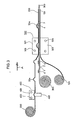
- FIG. 1 A semiconductor device of a preferred embodiment in accordance with the present invention is shown in Fig. 1 and in Fig. 2 which is a sectional view taken along the line II-II in Fig. 1.
- the semiconductor device comprises a first protecting member, that is, packing member 10, an electronic component 4, a second protecting member, that is, a packing member 20 and a plurality of lead wires 6.
- the first packing member 10 has a laminated structure comprising a reinforcing layer 1a, a metallic layer 2a and an insulating layer 3a.
- the reinforcing layer 1a is formed by imbuing glass fiber or the like with synthetic resin such as epoxy resin, and serves principally to maintain mechanical strength of the whole semiconductor device.
- the metallic layer 2a is formed by providing a metallic foil or metal evaporated film of aluminum or the like on the surface of the reinforcing layer 1a, and serves principally to prevent moisture and to shield from radioactive rays such as an a ray.
- the insulating layer 3a is formed by providing a high molecular weight material such as epoxy resin or a complex material of epoxy resin and polyester fiber, etc.
- the electronic component 4 is, for example, a semiconductor IC chip or the like and is attached on the surface of the insulating layer 3a of the above described first packing member through a die pad 5.
- the second packing member 20 has a convex portion 20a and the peripheral portion thereof is fixed to the above described first packing member. This convex portion 20a is positioned over the electronic component 4 so that a hollow portion 20b is formed to surround the electronic component 4.
- the second packing member 20 also has a laminated structure comprising a reinforcing layer 1b, a metallic layer 2b and an insulating layer 3b.
- the reinforcing layer 1b which serves principally to maintain mechanical strength of the whole semiconductor device, is formed by imbuing glass fiber or the like with synthetic resin such as epoxy resin.
- the metallic layer 2b which serves principally to prevent moisture and to shield from radioactive rays such as an a ray, is formed by providing a metallic foil or metal evaporated film of aluminum or the like on the surface of the reinforcing layer 1 b.
- the insulating layer 3b which serves to insulate the electronic component 4 from the exterior and to protect it from moisture, is formed by providing a high molecular weight material such as epoxy resin or a complex material of epoxy resin and polyester fiber etc. on the surface of the above described metallic layer 2b.
- Each of the lead wires 6 has one end exposed to the hollow portion 20b and the other end projecting outside the first and second packing members 10 and 20. These lead wires are fixed in an airtight manner by joining together by fusion the material of the insulating layer 3a of the first packing member and the material of the insulating layer 3b of the second packing member, at the time of fixing the peripheral portions of the first packing member 10 and the second packing member 20. Electrodes (not shown) formed on the surface of the electronic component 4 and the lead wires 6 corresponding thereto are electrically connected by means of bonding wires 7.
- the bonding wire is a gold wire or aluminum wire whose diameter is several tens of pm.
- the first and second packing members 10 and 20 Since the electronic component 4 is positioned in the hollow portion 20b sealed hermetically by the first packing member 10 and the second packing member 20, the first and second packing members 10 and 20 never touch the electronic component 4. This means that impurity contained in the insulating layers 3a and 3b of the first and second packing members 10 and 20, respectively, never exerts unfavorable influence on the electronic component 4. The unfavorable influence is for example, corrosion of the aluminum parts contained in the electronic component 4. Furthermore, at the time of manufacturing the semiconductor device the bonding wires 7 will never be distorted nor broken by contact with the protecting member. In addition, as a result of the above described structure, application of mechanical stress to the electronic component 4 can be prevented. Since the first and second packing members 10 and 20 include respectively metallic layers 2a and 2b, radioactive rays such as an a ray can be effectively shielded and accordingly, soft errors in the semiconductor device caused by such radioactive rays can be remarkably decreased.
- the materials for the respective layers constituting the first and second packing memberss 10 and 20 are not limited to the above described materials and may be the materials indicated in the following.
- the thickness of these layers is also indicated in the following.
- the materials described above in (i), (ii) or (iii) are to be used for a single layer or a laminated structure.
- the thickness of the reinforcing layer is not specifically limited to a certain value, but preferably, it is from 0.1 ⁇ m to 5000 pm.
- These metals or alloys are to be used as a single-layer metallic foil or as a laminated structure comprising a plurality of metallic foils of the same kind or different kinds.
- the thickess of a metallic layer is not specifically limited to a certain value, but preferably, it is from 1 pm to 3000 pm.
- organic material emitting little quantity of radioactive rays.
- organic material is for example as follows:
- thermosetting resin is for example as follows:
- the thickness is not specifically limited, but preferably it is from 0.1 pm to 3000 pm.
- the first and second packing members 10 and 20 each have a three-layer structure comprising a reinforcing layer, a metallic layer and an insulating layer.
- other structures may be adopted.
- a two-layer structure of a metallic layer and an insulating layer, a four-layer structure, a five-layer structure or the like may be used.
- the first and second packing member 10 and 20 are respectively of a laminated structure having a metallic layer and an insulating layer, a semiconductor device comprising such packing member is included in the present invention.
- the order of arrangement of the layers in the case of a three-layer structure is not limited to the above described example.
- a three-layer structure having a metallic layer as the outermost layer, a reinforcing layer as the intermediate layer and an insulating layer as the innermost layer may be adopted.
- the structure of the first packing member 10 and that of the second packing member 20 may be made different.
- the hollow portion 20b may be filled with gas.
- the gas to be used therein is for example a gas as indicated below:
- a hygroscopic material may be filled in the hollow portion 20b, or the wall of the hollow portion 20b may be coated with such material.
- hygroscopic material the following materials, for example, may be used:
- Such filling or coating serves to further improve the performance of a semiconductor device in accordance with the present invention.
- This semiconductor device can be manufactured by compression molding, inflation molding, forced molding or vacuum molding and the like. By using any one of these molding methods, a semiconductor device having a sufficient performance can be obtained. However, a more preferred manufacturing method provided by the inventors of the present invention will be described in the following.
- Fig. 3 shows a typical view of a manufacturing system of a semiconductor device shown in Figs. 1 and 2.
- a first packing member sheet 100 for forming a first packing member 10 of this semiconductor device a second packing member sheet for forming a second packing member 20 and a lead frame sheet 300 for forming lead wires 6 and die pads 7 are shown.
- the first packing member sheet 100 has a three-layer laminated structure comprised of a reinforcing layer 1a, a metallic layer 2a and an insulating layer 3a, corresponding to the structure of the first'packing member 10.
- the second packing member sheet 200 has also a three-layer laminated structure comprised of a reinforcing layer 1 b, a metallic layer 2b and an insulating layer 3b, corresponding to the structure of the second packing member 20. These three kinds of sheet are respectively wound in the form of a roll so as to be prepared for the manufacturing process. These rolls are gradually unwound, at the time of manufacturing semiconductor devices, so as to be extended in the direction shown by the arrow A in Fig. 3.
- a convexity forming device 400 forforming a convex portion 20a of the second packing member 20 is provided in the moving path of the second packing member sheet 200.
- a fixing device 500 for fixing these sheets is provided in a position where these three kinds of sheets are made to overlap.
- the convexity forming device 400 comprises an upper mold 401 having a spherical concavity, a lower mold 402 opposed to the upper mold 401 and having a spherical convexity fitted to the above stated concavity, and a heater 403 for heating the above stated upper mold 401.
- the fixing device 500 comprises an upper mold 501 having a spherical concavity corresponding to the convex portion 20a formed in the second packing member sheet 200, a lower mold 502 opposed to the upper mold 501 and heaters 503 and 504 respectively attached to the upper mold 501 and the lower mold 502.
- the second packing member sheet 200 is insertd between the upper mold 401 and the lower mold 402 of the concavity forming device 400.
- This second packing member sheet 200 is pressed between the upper mold 401 heated by the heater 403 and the lowr mold 402, so that a convex portion 20a is formed in the second packing member sheet 200.
- This pressing operation is made intermittently while the second packing member sheet 200 is set, whereby convex portions 20a are successively formed in the second packing member sheet 200 at predetermined intervals.
- the lead frame sheet 300 is gradually unwound, so that die bonding operation and wire bonding operation for electric components 4 are made on the surface thereof.
- electronic components 4 are attached successively on the surface of the lead frame sheet 300 at predetermined intervals.
- Each electronic component 4 is formed on a die pad 5 of the lead frame sheet 300.
- the intervals at which the electronic components 4 are formed are the same as the intervals at which the convex portions 20a are formed on the second packing member sheet 200.
- the second packing member sheet 200 having convex portions 20a, the lead frame sheet 300 with electronic components 4 formed thereon and the first packing member sheet 100 are put together in an overlapping manner in this order, so that the overlapping sheets are inserted between the upper mold 501 and the lower mold 502 of the fixing device 500.
- the convex portion 20a of the second packing member sheet 200 is to cover up the electronic component 4 in a state where a hollow portion 20b is formed over the electronic component 4 as shown in Fig. 2, the relative positioning between the second packing member sheet 200 and the lead frame sheet 300 is adjusted so that each convex portion 20a may be positioned just above the corresponding electronic component 4 and bonding wire 7 and each convex portion 20a may not touch them to cause deformation thereto at the time of fixing.
- the upper mold 501 and the lower mold 502 of the fixing device 500 are heated by the heaters 503 and 504, respectively, at the temperature 100 to 250°C. This temperature is suited for curing the epoxy resin included in the insulating layers 3a and 3b of the first and second packing members.
- the thickness of the lead frame sheet 300 is as small as 0.5 mm and the epoxy resin contained in the insulating layers 3a and 3b of the first and second packing member sheets 100 and 200 is sufficiently softened by heating and application of pressure, these insulating layers are joined together by fusion so that the lead frame sheet 300 is completely sealed in an airtight manner.
- airtight sealing of the electronic component 4 is realized.
- the above described pressure fixing operation is made intermittently, that is, each time a convex portion 20a arrives just below the concave portion of the upper mold 501.
- the three kinds of sheets thus stuck together by fusion to be one body are moved in the direction of the arrow A so as to be cut.
- a semiconductor device shown in Figs. 1 and 2 is obtained.
- Fig. 4 shows a sectional view of a conventional semiconductor device sealed with a sealing resin 8.
- the semiconductor devices used in the below described tests were manufactured by using EME500 (made by Sumitomo Bakelite Co., Ltd. in Chiyoda-ku, Tokyo, Japan) as the sealing resin 8 and bipolar type ICs, C51521, C53206 and a MOS IC, C5G1400 (all made by Mitusbishi Electric Corp. In Chiyoda-ku, Tokyo, Japan) as the electronic components 4.
- Semiconductor devices are exposed to the atmosphere under the conditions of temperature 120°C, atmospheric pressure of 2 atm and humidity 100% for 5000 hours.
- Semiconductor devices are exposed to the temperature of -55°C for 30 minutes and then exposed to the temperature of 125°C for 30 minutes. This cycle is repeated 200 times.
- Semiconductor devices are exposed to the temperature of -190°C for 5 minutes and then exposed to the temperature of 260°C for 5 minutes. This cycle is repeated 50 times.
- test 4 Moisture Resistant Reverse Bias Test
- Reverse voltage of 10 volts is applied to semiconductor devices in the atmosphere under the conditions of temperature 120°C, atmospheric pressure of 2 atm and humidity 100% and this state is maintained for 100 hours.
- Table 2 shows percents of defectiveness obtained as a result of the above described four tests concerning the semiconductor devices in which the above described materials are used.
- the semiconductor devices of the embodiments 1 to 3 in accordance with the present invention exhibit by far more excellent characteristics in all the above described four tests as compared with the semiconductor devices of the conventional types 1 to 3. More specifically stated, since metallic layers 2a and 2b made of aluminum foil are provided in the embodiments of the present invention, the moisture resistant characteristic is improved and accordingly, the performance with respect to the moisture resistant test and the moisture resistant reverse bias test is heightened.
- the hollow portion 20b is formed by the convex portion 20a of the second packing member 20, stress is hardly applied to the electronic component 4, which serves to improve the performance with respect to the heat cycle test and heat shock test. Since the convex portion 20a of the second packing member 20 does not touch the electronic component 4, the aluminum electrodes formed on the surface of the electronic component 4 are hardly subjected to corrosion.
- the semiconductor devices of the embodiments have also eminently excellent characteristics in all the tests, as in the case of the semiconductor devices of the embodiments 1 to 3, compared with the semiconductor device of the conventional type 3. It is understood that the characteristics of the semiconductor devices in accordance with the present invention undergo little influence even if the materials for the reinforcing layers 1a, 1b, the metallic layers 2a, 2b and the insulating layers 3a, 3b of the first and second packing members 10 and 20 are replaced by other materials indicated above. In addition, it will be clearly understood that the same results can be obtained even if combinations other than these shown in Table 3 are adopted for the combinations of the insulating layers 3a and 3b and the reinforcing layers 1a and 1b.
- the semiconductor devices of the embodiments 11 to 15 have also eminently excellent characteristics, as in the devices of the embodiments 3 to 10, as compared with the device of the conventional type 3.
- the semiconductor devices with the thickness of the layers of the first and second packing members 10 and 20 being changed for each embodiment exhibit also eminently excellent characteristics in either of the tests concerning the moisture resistance, as in the case of the device of the embodiment 3, compared with the device of the conventional type 3.
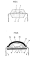
- the first and second packing members 10 and 20 each comprise a three-layer structure having reinforcing layers 1a and 1b, metallic layers 2a and 2b and insulating layers 3a and 3b.
- the first and second packing members each comprise a two-layer structure as shown in Fig. 5. More specifically, two-layer structures respectively comprising metallic layers 2a and 2b an insulating layers 3a and 3b are provided for the first and second packing members 10 and 20, by making the metallic layers 2a and 2b perform also the functions of the reinforcing layers 1a and 1b.
- the semiconductor devices of the embodiments 20 to 25 also have eminently excellent characteristics as compared with the device of the conventional type 3, and such excellent characteristics can be obtained independently of the nature of metal used for the metallic layers 2a and 2b of the first and second packing members 10 and 20.
- the thickness of the first packing member 10 is larger than that of the first packing member of the device shown in Figs. 1 and 2, say, approximately 1.6 mm, and a hollow portion, is formed on the side of the insulating layer 3b of the second packing member 20, the reinforcing layer 1b having a plane surface.
- This plane surface of the reinforcing layer 1b is obtained by forming a convex portion in the second packing member sheet 200 by means of the convexity forming device 400 shown in Fig. 3 and flattening the convex portion of the reinforcing layer 1 b so as to make plane the whole surface of the reinforcing layer 1 b.
- the semiconductor devices of the embodiments 26 to 33 also exhibit eminently excellent characteristics in all the tests, as compared with the device of the conventional type 3.
- the first and second packing members 10 and 20 both have a thickness larger than that of the first packing member and the second packing member of the device shown in Figs. 1 and 2, and the thickness in these embodiments 34 to 41 is for example 1.6 mm.
- a convex portion is provided respectively in the first and second packing members 10 and 20, whereby a hollow portion is formed to extend over and under the electronic component 4.
- the respective outside surfaces of the reinforcing layers 1a and 1b are made plane.
- the semiconductor devices of the embodiments 34 to 41 also exhibit eminently excellent characteristics in all the tests as in the device of the embodiment 3, compared with the device of the conventional type 3.
- This embodiment 42 is a semiconductor device in which a 64K dynamic RAM not coated with any organic material is used as the electronic component 4 and the same structures as in the embodiments 1 to 3 are adopted for the other portions.
- a semiconductor device in accordance with the present invention has an excellent performance for prevention of soft error.
- the first and second packing members 10 and 20 contain respectively the metallic layers 2a and 2b which prevent transmission of the a ray and the materials of the insulating layers 3a and 3b and reinforcing layers 1 a and 1b of the first and second packing members 10 and 20 do not include inorganic materials containing uranium or thorium.
- the semiconductor device of the embodiment 42 shows excellent results in the tests 1 to 4, as in the above described embodiment 1 to 3.
- the first packing member 10 and the second packing member 20 may be stuck together using an adhesive.
Landscapes
- Engineering & Computer Science (AREA)
- Computer Hardware Design (AREA)
- Microelectronics & Electronic Packaging (AREA)
- Power Engineering (AREA)
- Physics & Mathematics (AREA)
- Condensed Matter Physics & Semiconductors (AREA)
- General Physics & Mathematics (AREA)
- Manufacturing & Machinery (AREA)
- Structures Or Materials For Encapsulating Or Coating Semiconductor Devices Or Solid State Devices (AREA)
Description
- The present invention relates to a semiconductor device and particularly to a semiconductor device comprising packing members having novelty for protecting semiconductor elements and other electronic components from external environment.
- In general, a semiconductor device comprises a structure in which semiconductor elements and electronic components such as an integrated circuit (referred to hereinafter as an IC), transistors, diodes, capacitors, resistors, a hybrid IC, microcoils, etc are provided on one substrate or more. A semiconductor device comprising such elements and components is normally of a considerably small size and as a result, is liable to undergo physical or chemical influences due to the external environment. In order to prevent such influences and to assure stability and a long life, a semiconductor device is normally provided with protecting means. Such protecting means is formed so as to wrap the semiconductor elements and electronic components, for the purpose of protection.
- One of the conventional protecting means widely utilized is formed by an airtight sealing method, in which metal or ceramic is used. A notable increase of production of semiconductor devices in these days has led to the use of a resin sealing method utilizing organic materials, instead of the above mentioned airtight sealing method. As the resin sealing method, a transfer molding method is applied in which a molding material heated and softened in advance is compressed into a heated metallic mold by means of a press. As the molding material for use in this transfer molding method, epoxy resin or silicone resin mixed with a curing agent, a bulking agent, a flame resistant agent, a coupling agent and a coloring agent is utilized. In particular, a mixture composed principally of epoxy resin is utilized in many types of semiconductor devices, because this mixture of epoxy resin has various excellent characteristics.
- In a semiconductor device provided with protecting means formed by the transfer molding method using as the molding material a mixture composed principally of epoxy resin, IC and other semiconductor elements and electronic components are in a state completely sealed with resin. As a result, tips and bonding wires of the IC etc. are directly in contact with the resin and accordingly, such a semiconductor device provided with protecting means formed by the resin sealing method has excellent characteristics in moisture resistance, heat conductivity, shock resistance and the like, as compared with a semiconductor device sealed by an airtight sealing method using metal or ceramic.
- However, a remarkably high degree of integration of circuits attained recently results in a demand for realizing a semiconductor device having a higher reliability with respect to the above stated characteristics and other characteristics. In order to satisfy such demand, it is requested: (i) to improve moisture resistance; (ii) to prevent the electronic components from being broken due to curing stress of the sealing material, that is, a resin; (iii) to derease soft errors in the semiconductor device, caused by X rays radiating from the sealing material; (iv) to prevent falling down of gold wires in the electronic components, which could be caused by a resin having a high viscosity at the time of resin sealing by a transfer molding method; and to take other measures. With a view to complying with these requests in a conventional semiconductor device comprising protecting means formed by a transfer molding method using a mixture of epoxy resin, the purity of resins or bulking agents has been enhanced and the types and mixing quantity of a catalyzer or a surface treatment agent as well as the manufacturing process for resin sealing have been re-examined, which has brought about an improvement of the performance to a certain degree. However, there is a limit in such improvement.
- More specifically stated, concerning the improvement of moisture resistance as described above in (i), there are problems as follows. Deterioration due to moisture in a semiconductor device is caused principally by moisture penetrating through two paths, that is, moisture infiltrating a resin layer and moisture penatrating through a surface of contact between the resin layer and the lead wires. The moisture penetrating through these paths dissolves therein impurity contained in the sealing resin, so that the moisture itself is made alkaline or acid. This moisture reaches to the aluminum electrodes formed on the surface of the electronic components, causing corrosion in the aluminum electrodes. For this reason, in order to improve moisture resistance, efforts have been made to improve the purity of resins and bulking agents, re-examine the types and mixing quantity of a catalyzer or a coupling agent, improve the processing method for these materials, etc., and actually, an improvement of the performance has been realized to a certain degree. However, as long as a resin which is permeable by water is used, the moisture penetrating to the surface of the electronic component cannot be completely removed.
- Damage or distortion in the electronic components, caused by curing stress of a sealing material, as described above in (ii) can be minimized by decreasing the difference between the coefficient of linear expansion of the material of an electronic component, e.g. a wafer for IC, and that of a resin used as sealing material. The decrease in the difference between the coefficients of linear expansion is generally made by adding a bulking agent such as silica into the resin. However, it is substantially difficult to make no difference exist between the coefficients of linear expansion of the resin and the electronic component by adding a large quantity of bulking agent into the resin. In addition, unfavorably, the bulking agent added for the purpose of decreasing the stress contains thorium, uranium and the like, and radioactive rays emitted from these substances, particularly the a ray would cause soft errors in the electronic component.
- According to the invention there is provided a semiconductor device comprising:
- a first laminated structure having a first metallic layer and a first insulating layer,
- a second laminated structure having a second metallic layer and a second insulating layer,
- said first and second laminated structures being positioned with their insulating layers facing each other and the respective peripheral portions thereof being connected with each other in an airtight manner, so that said first and second laminated structures are interconnected in a state whereby an airtight hollow portion substantially surrounded by said first and second metallic layers and by said first and second insulating layers is formed therebetween,
- an electronic component comprising a semiconductor element provided inside said hollow portion, and
- at least one lead means interposed in the boundary of connection between said first insulating layer and said second insulating layer, one end of said lead means extending into said hollow portion so as to be electrically connected to said electronic component and the other end thereof extending from said boundary of connection to the exterior.
- There are described below preferred embodiments of the present invention which exhibit the advantages that the semiconductor device has an excellent moisture resistance, the electronic components are not damaged by curing stress of the sealing material, that soft errors in the electronic components scarcely occur due to radioactive rays, and that the semiconductor device can be easily manufactured without using a press or metallic molds.
-
- Fig. 1 is a perspective view showing a stucture of a semiconductor device of an embodiment in accordance with the present invention.
- Fig. 2 is a sectional view of the semiconductor device in Fig. 1 taken along the line II-II.
- Fig. 3 is a view for explaining a method of manufacturing the semiconductor device shown in Figs. 1 and 2.
- Fig. 4 is a sectional view of a conventional semiconductor device.
- Fig. 5, 6 and 7 ar views showing respectively semiconductor devices of other embodiments in accordance with the present invention.
- A semiconductor device of a preferred embodiment in accordance with the present invention is shown in Fig. 1 and in Fig. 2 which is a sectional view taken along the line II-II in Fig. 1. Referring to these drawings, the semiconductor device comprises a first protecting member, that is, packing
member 10, anelectronic component 4, a second protecting member, that is, apacking member 20 and a plurality oflead wires 6. - The
first packing member 10 has a laminated structure comprising a reinforcing layer 1a, ametallic layer 2a and aninsulating layer 3a. The reinforcing layer 1a is formed by imbuing glass fiber or the like with synthetic resin such as epoxy resin, and serves principally to maintain mechanical strength of the whole semiconductor device. Themetallic layer 2a is formed by providing a metallic foil or metal evaporated film of aluminum or the like on the surface of the reinforcing layer 1a, and serves principally to prevent moisture and to shield from radioactive rays such as an a ray. Theinsulating layer 3a is formed by providing a high molecular weight material such as epoxy resin or a complex material of epoxy resin and polyester fiber, etc. on the surface of the above describedmetallic layer 2a, and serves principally to insulate theelectronic component 4 from the exterior and to prevent moisture. Theelectronic component 4 is, for example, a semiconductor IC chip or the like and is attached on the surface of theinsulating layer 3a of the above described first packing member through adie pad 5. Thesecond packing member 20 has aconvex portion 20a and the peripheral portion thereof is fixed to the above described first packing member. Thisconvex portion 20a is positioned over theelectronic component 4 so that ahollow portion 20b is formed to surround theelectronic component 4. Thesecond packing member 20 also has a laminated structure comprising a reinforcinglayer 1b, ametallic layer 2b and aninsulating layer 3b. The reinforcinglayer 1b, which serves principally to maintain mechanical strength of the whole semiconductor device, is formed by imbuing glass fiber or the like with synthetic resin such as epoxy resin. Themetallic layer 2b, which serves principally to prevent moisture and to shield from radioactive rays such as an a ray, is formed by providing a metallic foil or metal evaporated film of aluminum or the like on the surface of the reinforcinglayer 1 b. The insulatinglayer 3b, which serves to insulate theelectronic component 4 from the exterior and to protect it from moisture, is formed by providing a high molecular weight material such as epoxy resin or a complex material of epoxy resin and polyester fiber etc. on the surface of the above describedmetallic layer 2b. Each of thelead wires 6 has one end exposed to thehollow portion 20b and the other end projecting outside the first andsecond packing members insulating layer 3a of the first packing member and the material of the insulatinglayer 3b of the second packing member, at the time of fixing the peripheral portions of thefirst packing member 10 and thesecond packing member 20. Electrodes (not shown) formed on the surface of theelectronic component 4 and thelead wires 6 corresponding thereto are electrically connected by means ofbonding wires 7. The bonding wire is a gold wire or aluminum wire whose diameter is several tens of pm. - Since the
electronic component 4 is positioned in thehollow portion 20b sealed hermetically by thefirst packing member 10 and thesecond packing member 20, the first andsecond packing members electronic component 4. This means that impurity contained in theinsulating layers second packing members electronic component 4. The unfavorable influence is for example, corrosion of the aluminum parts contained in theelectronic component 4. Furthermore, at the time of manufacturing the semiconductor device thebonding wires 7 will never be distorted nor broken by contact with the protecting member. In addition, as a result of the above described structure, application of mechanical stress to theelectronic component 4 can be prevented. Since the first andsecond packing members metallic layers - The materials for the respective layers constituting the first and
second packing memberss -
- (i) Fiber of glass, ceramic, asbestos, mica, metal, paper or the like
- (i) Sheet imbued with one thermosetting resin or more. The thermosetting resins to be used are for example as follows: epoxy resin, silicone resin, phenol resin, diallyl patalate resin, melamine resin, unsaturated polyester resin, and polyurethane resin.
- (iii) Film of a thermoplastic resin or combination of such film and the above stated fiber or thermosetting resin. The thermoplastic resin is for example as follows: polyethylene, polypropylene, polyvinyl acetal, ethylene 4-fluoride, polyphenylene sulfide, polyvinyl chloride, polystyrene, acrylic, polyvinyl alcohol, polyether ether ketone, polyimide, polyamide imide, polyamide, polysulfone, polycarbonate, saturated polyester.
- The materials described above in (i), (ii) or (iii) are to be used for a single layer or a laminated structure. The thickness of the reinforcing layer is not specifically limited to a certain value, but preferably, it is from 0.1 µm to 5000 pm.
- Aluminum, copper, gold, iron, stainless steel, tin, lead, titanium, cobalt, nickel, tungsten, antimony, hastelloy, inconel, zinc, magnesium and alloys thereof.
- These metals or alloys are to be used as a single-layer metallic foil or as a laminated structure comprising a plurality of metallic foils of the same kind or different kinds. The thickess of a metallic layer is not specifically limited to a certain value, but preferably, it is from 1 pm to 3000 pm.
- It is desired to use an organic material emitting little quantity of radioactive rays. Such organic material is for example as follows:
- Fiber or film of polyester, polyamide, polyethylene, polypropylene, ethylene 4-fluoride, polyimide, polyacetal, polyvinyl chloride, polycarbonate, polysulfin, polyether either ketone, polyphenylene sulfide and cellulosic material such as paper and the like.
- These materials may be used singly or together with a thermosetting resin. Such thermosetting resin is for example as follows:
- Epoxy resin, silicone resin, unsaturated polyester resin, phenol resin, melamine resin, diallyl phtalate resin, urea resin, and polyurethane resin.
- The thickness is not specifically limited, but preferably it is from 0.1 pm to 3000 pm.
- The materials shown above in (a) to (c) were indicated by way of example only, and should not be taken in a limitative sense.
- In the above described embodiment, the first and
second packing members electronic component 4 and the characteristics required for it, other structures may be adopted. For example, a two-layer structure of a metallic layer and an insulating layer, a four-layer structure, a five-layer structure or the like may be used. So long as the first and second packingmember first packing member 10 and that of thesecond packing member 20 may be made different. - In addition, the
hollow portion 20b may be filled with gas. The gas to be used therein is for example a gas as indicated below: - Inert gas such as helium, neon, argon, xenon, krypton and the like or nitrogen gas.
- A hygroscopic material may be filled in the
hollow portion 20b, or the wall of thehollow portion 20b may be coated with such material. As such hygroscopic material, the following materials, for example, may be used: - Silica gel, cobalt chloride, phosphorus pentoxide, polyvinyl alcohol and cellulosic material.
- Such filling or coating serves to further improve the performance of a semiconductor device in accordance with the present invention.
- Now, a method of manufacturing of a semiconductor device shown in Figs. 1 and 2 will be described. This semiconductor device can be manufactured by compression molding, inflation molding, forced molding or vacuum molding and the like. By using any one of these molding methods, a semiconductor device having a sufficient performance can be obtained. However, a more preferred manufacturing method provided by the inventors of the present invention will be described in the following.
- Fig. 3 shows a typical view of a manufacturing system of a semiconductor device shown in Figs. 1 and 2. Referring to Fig. 3 as well as Figs. 1 and 2, a first
packing member sheet 100 for forming afirst packing member 10 of this semiconductor device, a second packing member sheet for forming asecond packing member 20 and alead frame sheet 300 for forminglead wires 6 and diepads 7 are shown. The firstpacking member sheet 100 has a three-layer laminated structure comprised of a reinforcing layer 1a, ametallic layer 2a and an insulatinglayer 3a, corresponding to the structure of the first'packingmember 10. The secondpacking member sheet 200 has also a three-layer laminated structure comprised of a reinforcinglayer 1 b, ametallic layer 2b and an insulatinglayer 3b, corresponding to the structure of thesecond packing member 20. These three kinds of sheet are respectively wound in the form of a roll so as to be prepared for the manufacturing process. These rolls are gradually unwound, at the time of manufacturing semiconductor devices, so as to be extended in the direction shown by the arrow A in Fig. 3. In the moving path of the secondpacking member sheet 200, aconvexity forming device 400 forforming aconvex portion 20a of thesecond packing member 20 is provided. In a position where these three kinds of sheets are made to overlap, a fixingdevice 500 for fixing these sheets is provided. Theconvexity forming device 400 comprises anupper mold 401 having a spherical concavity, alower mold 402 opposed to theupper mold 401 and having a spherical convexity fitted to the above stated concavity, and aheater 403 for heating the above statedupper mold 401. The fixingdevice 500 comprises anupper mold 501 having a spherical concavity corresponding to theconvex portion 20a formed in the secondpacking member sheet 200, alower mold 502 opposed to theupper mold 501 andheaters upper mold 501 and thelower mold 502. - In the manufacturing process, first, the second
packing member sheet 200 is insertd between theupper mold 401 and thelower mold 402 of theconcavity forming device 400. This secondpacking member sheet 200 is pressed between theupper mold 401 heated by theheater 403 and thelowr mold 402, so that aconvex portion 20a is formed in the secondpacking member sheet 200. This pressing operation is made intermittently while the secondpacking member sheet 200 is set, wherebyconvex portions 20a are successively formed in the secondpacking member sheet 200 at predetermined intervals. On the other hand, thelead frame sheet 300 is gradually unwound, so that die bonding operation and wire bonding operation forelectric components 4 are made on the surface thereof. As a result,electronic components 4 are attached successively on the surface of thelead frame sheet 300 at predetermined intervals. Eachelectronic component 4 is formed on adie pad 5 of thelead frame sheet 300. The intervals at which theelectronic components 4 are formed are the same as the intervals at which theconvex portions 20a are formed on the secondpacking member sheet 200. Then, the secondpacking member sheet 200 havingconvex portions 20a, thelead frame sheet 300 withelectronic components 4 formed thereon and the firstpacking member sheet 100 are put together in an overlapping manner in this order, so that the overlapping sheets are inserted between theupper mold 501 and thelower mold 502 of the fixingdevice 500. Since theconvex portion 20a of the secondpacking member sheet 200 is to cover up theelectronic component 4 in a state where ahollow portion 20b is formed over theelectronic component 4 as shown in Fig. 2, the relative positioning between the secondpacking member sheet 200 and thelead frame sheet 300 is adjusted so that eachconvex portion 20a may be positioned just above the correspondingelectronic component 4 andbonding wire 7 and eachconvex portion 20a may not touch them to cause deformation thereto at the time of fixing. Theupper mold 501 and thelower mold 502 of the fixingdevice 500 are heated by theheaters temperature 100 to 250°C. This temperature is suited for curing the epoxy resin included in the insulatinglayers convex portions 20a of the secondpacking member sheet 200 arrives just below the concave portion of theupper mold 501, theupper mold 501 and thelower mold 502 operate to press these overlapping sheets, whereby the first and secondpacking member sheets lead frame sheet 300, respectively. Thus, these three kinds of sheets are struck together in the state where theelectronic component 4 is disposed inside thehollow portion 20b covered with theconvex portion 20a of the second packing member sheet. At this time, since the thickness of thelead frame sheet 300 is as small as 0.5 mm and the epoxy resin contained in the insulatinglayers packing member sheets lead frame sheet 300 is completely sealed in an airtight manner. Thus, airtight sealing of theelectronic component 4 is realized. The above described pressure fixing operation is made intermittently, that is, each time aconvex portion 20a arrives just below the concave portion of theupper mold 501. The three kinds of sheets thus stuck together by fusion to be one body are moved in the direction of the arrow A so as to be cut. By bending the lead wires into a desired form, a semiconductor device shown in Figs. 1 and 2 is obtained. - Now, the performance of a semiconductor device in accordance with an embodiment of the present invention will be described as compared with the performance of a conventional semiconductor device.
- Fig. 4 shows a sectional view of a conventional semiconductor device sealed with a sealing
resin 8. The semiconductor devices used in the below described tests were manufactured by using EME500 (made by Sumitomo Bakelite Co., Ltd. in Chiyoda-ku, Tokyo, Japan) as the sealingresin 8 and bipolar type ICs, C51521, C53206 and a MOS IC, C5G1400 (all made by Mitusbishi Electric Corp. In Chiyoda-ku, Tokyo, Japan) as theelectronic components 4. - Concerning the above described conventional semiconductor devices, the following four tests were made. In each of the tests, one hundred semiconductor devices were used.
- Semiconductor devices are exposed to the atmosphere under the conditions of temperature 120°C, atmospheric pressure of 2 atm and
humidity 100% for 5000 hours. - Semiconductor devices are exposed to the temperature of -55°C for 30 minutes and then exposed to the temperature of 125°C for 30 minutes. This cycle is repeated 200 times.
- Semiconductor devices are exposed to the temperature of -190°C for 5 minutes and then exposed to the temperature of 260°C for 5 minutes. This cycle is repeated 50 times.
- Reverse voltage of 10 volts is applied to semiconductor devices in the atmosphere under the conditions of temperature 120°C, atmospheric pressure of 2 atm and
humidity 100% and this state is maintained for 100 hours. - These tests were made using the conventional semiconductor devices structured as described above and as a result, percentage or defectiveness in each of the tests was found as shown in the following table.

- The above described tests were made as to the semiconductor device having the structure shown in Fig. 2, using the below described materials for the respective portions. In each of tests, one hundred semiconductor devices were used.,
- (1) Reinforcing
layers 1a and 1b of the first andsecond packing members - (2)
Metallic layers second packing members - (3) Insulating
layers second packing members - (4)
Electronic components 4 ... Bipolar type IC, C51521 (embodiment 1), C53206 (embodiment 2) and MOS IC, C5G1400 (embodiment 3). - Table 2 shows percents of defectiveness obtained as a result of the above described four tests concerning the semiconductor devices in which the above described materials are used.

- As is clearly understood from the comparison of Table 1 and Table 2, the semiconductor devices of the embodiments 1 to 3 in accordance with the present invention exhibit by far more excellent characteristics in all the above described four tests as compared with the semiconductor devices of the conventional types 1 to 3. More specifically stated, since
metallic layers hollow portion 20b is formed by theconvex portion 20a of thesecond packing member 20, stress is hardly applied to theelectronic component 4, which serves to improve the performance with respect to the heat cycle test and heat shock test. Since theconvex portion 20a of thesecond packing member 20 does not touch theelectronic component 4, the aluminum electrodes formed on the surface of theelectronic component 4 are hardly subjected to corrosion. - Concerning the semiconductor device shown in Fig. 2, structured by using the below indicated materials, the above described tests 1 to 4 were made and the percentages of defectiveness shown in Table 4 were obtained. Table 3 given below shows combinations of the materials in the
embodiments 4 to 10. - (1) Reinforcing
layers 1a and 1b and insulatinglayers second packing members - (a) Epoxy resin ... novolak-type epoxy resin, ESCN220HH (made by Sumitomo Chemical Co., Ltd. in Osaka Prefecture, Japan), ECON-102 (made by Nihan Kayaku Co., Ltd. in Chiyoda-ku, Tokyo, Japan) DEN438 (made by the Dow Chemical Co., U.S.A.), Epikote 1001 Triglycidylisocyanurate TG1C (made by Shell Oil Co., U.S.A.) or (made by Ciba Geigy A.G. Switzerland).
- (b) Curing agent... phenol novolak, PSK4300 (made by Gunei Chemical Industry Co., Ltd. In Takasaki City, Gunma Prefecture, Japan) or anhydrous trimellitic acid diamino-diphenyl methane.
- (c) Fiber, film or mat... fiber, film or mat of glass or phoyester.
- (2)
Metallic layers second packing members - (3)
Electronic component 4 ... MOS IC, C5G1400

- As can be seen from Table 4, the semiconductor devices of the embodiments have also eminently excellent characteristics in all the tests, as in the case of the semiconductor devices of the embodiments 1 to 3, compared with the semiconductor device of the conventional type 3. It is understood that the characteristics of the semiconductor devices in accordance with the present invention undergo little influence even if the materials for the reinforcing
layers 1a, 1b, themetallic layers layers second packing members layers layers 1a and 1b. - In the above described embodiments 3 to 10, combinations of organic materials are used as the materials for forming the insulating
layers second packing members layers - Concerning the semiconductor devices of the embodiments 11 to 15, structured by using the below indicated materials, the above described four tests were made and the percentages of defectiveness shown in Table 6 were obtained.
- (1) Reinforcing
layers 1a and 1b and insulatinglayers second packing members - (2) Materials of the other layers ... Combinations shown in Table 5.
- (3) Electronic component and other portions ... Same as in the embodiments 3 to 10


- As can be seen from Table 6, the semiconductor devices of the embodiments 11 to 15 have also eminently excellent characteristics, as in the devices of the embodiments 3 to 10, as compared with the device of the conventional type 3.
- Concerning the semiconductor devices of the embodiments 16 to 19, manufactured by using the below indicated materials, the
tests 1 and 4 were made and the results shown in Table 7 were obtained. - (1)
Metallic layers second packing members - (2) Materials and structures of other portions ... Same as in the device of the embodiment 3

- As is seen from Table 7, the semiconductor devices with the thickness of the layers of the first and
second packing members - In the respective devices of the above described embodiments 1 to 3, the first and
second packing members layers 1a and 1b,metallic layers layers embodments 20 to 25, the first and second packing members each comprise a two-layer structure as shown in Fig. 5. More specifically, two-layer structures respectively comprisingmetallic layers layers second packing members metallic layers layers 1a and 1b. - The below indicated materials were used for forming the respective portions of a device and the tests 1 to 4 were made with respect to the semiconductor devices thus formed. The percentages of defectiveness obtained by the tests are shown in Table 9.
- (1)
Metallic layers second packing members - (2) Isulating layers 3a and 3b of the first and
second packing members - (3) Materials and structures of other portions ... Same as in the device of the embodiment 3, except that the reinforcing
layers 1 a and 1 b as in the embodiment 3 are not provided specially.

- As is understood from Table 9, the semiconductor devices of the
embodiments 20 to 25 also have eminently excellent characteristics as compared with the device of the conventional type 3, and such excellent characteristics can be obtained independently of the nature of metal used for themetallic layers second packing members - In these embodiments, as shown in Fig. 6, the thickness of the
first packing member 10 is larger than that of the first packing member of the device shown in Figs. 1 and 2, say, approximately 1.6 mm, and a hollow portion, is formed on the side of the insulatinglayer 3b of thesecond packing member 20, the reinforcinglayer 1b having a plane surface. This plane surface of the reinforcinglayer 1b is obtained by forming a convex portion in the secondpacking member sheet 200 by means of theconvexity forming device 400 shown in Fig. 3 and flattening the convex portion of the reinforcinglayer 1 b so as to make plane the whole surface of the reinforcinglayer 1 b. - Concerning the semiconductor devices in which the combinations of materials shown in Table 10 are used for the reinforcing
layers 1a and 1b,metallic layers layers layer 1b is made plane as described above and the same materials and structures as in the embodiment 3 are adopted for the other portions, the tests 1 to 4 were performed and the percentages of defectiveness obtained as the results of the tests are shown in Table 11.

- As can be seen from Table 11, the semiconductor devices of the embodiments 26 to 33 also exhibit eminently excellent characteristics in all the tests, as compared with the device of the conventional type 3.
- In these embodiments, as shown in Fig. 7, the first and
second packing members second packing members electronic component 4. The respective outside surfaces of the reinforcinglayers 1a and 1b are made plane. - Concerning the semiconductor devices in which combinations of materials shown in Table 12 are used for the reinforcing
layers 1a and 1b,metallic layers layers layers 1a and 1b being made plane as described above, and the same materials and structures as in the embodiment 3 are adopted for the other portions, the tests 1 to 4 were performed and the percentages of defectiveness obtained as the results thereof are shown in Table 13.

- As can be seen from Table 13, the semiconductor devices of the embodiments 34 to 41 also exhibit eminently excellent characteristics in all the tests as in the device of the embodiment 3, compared with the device of the conventional type 3.
- This embodiment 42 is a semiconductor device in which a 64K dynamic RAM not coated with any organic material is used as the
electronic component 4 and the same structures as in the embodiments 1 to 3 are adopted for the other portions. - One hundred devices of this type were manufactured and after they were left for 1000 hours, percentage of occurrence of soft error, that is, soft error ratio in each of them was examined. As a result, it was found that there was no semiconductor device causing soft error.
- On the other hand, a soft error ration of 8% was obtained by the examination of the conventional semiconductor devices ("
conventional device 4") in which the above described component was used as theelectronic component 4 and the same structures as in the conventional types 1 to 3 were adopted for the other portions. - Accordingly, it is understood that a semiconductor device in accordance with the present invention has an excellent performance for prevention of soft error. This is because the first and
second packing members metallic layers layers layers 1 a and 1b of the first andsecond packing members - Although an IC was used as an
electronic component 4 in the above described embodiment 1 to 42, the same results can be obtained if a diode, a transistor or the like is used. Thefirst packing member 10 and thesecond packing member 20 may be stuck together using an adhesive. - Although the present invention has been described and illustrated in detail, it is clearly understood that the same is by way of illustration and example only and is not to be taken by way of limitation, the scope of the present invention being limited only by the terms of the appended claims.
Claims (13)
Applications Claiming Priority (2)
| Application Number | Priority Date | Filing Date | Title |
|---|---|---|---|
| JP46153/83 | 1983-03-18 | ||
| JP58046153A JPS59172253A (en) | 1983-03-18 | 1983-03-18 | Semiconductor device |
Publications (3)
| Publication Number | Publication Date |
|---|---|
| EP0122687A2 EP0122687A2 (en) | 1984-10-24 |
| EP0122687A3 EP0122687A3 (en) | 1986-01-15 |
| EP0122687B1 true EP0122687B1 (en) | 1988-11-02 |
Family
ID=12739035
Family Applications (1)
| Application Number | Title | Priority Date | Filing Date |
|---|---|---|---|
| EP84300521A Expired EP0122687B1 (en) | 1983-03-18 | 1984-01-27 | A semiconductor device comprising packing means for protecting parts of the device |
Country Status (4)
| Country | Link |
|---|---|
| US (1) | US4717948A (en) |
| EP (1) | EP0122687B1 (en) |
| JP (1) | JPS59172253A (en) |
| DE (1) | DE3475031D1 (en) |
Cited By (13)
| Publication number | Priority date | Publication date | Assignee | Title |
|---|---|---|---|---|
| US6919626B2 (en) | 1992-12-11 | 2005-07-19 | Staktek Group L.P. | High density integrated circuit module |
| US7026708B2 (en) | 2001-10-26 | 2006-04-11 | Staktek Group L.P. | Low profile chip scale stacking system and method |
| US7066741B2 (en) | 1999-09-24 | 2006-06-27 | Staktek Group L.P. | Flexible circuit connector for stacked chip module |
| US7289327B2 (en) | 2006-02-27 | 2007-10-30 | Stakick Group L.P. | Active cooling methods and apparatus for modules |
| US7324352B2 (en) | 2004-09-03 | 2008-01-29 | Staktek Group L.P. | High capacity thin module system and method |
| US7443023B2 (en) | 2004-09-03 | 2008-10-28 | Entorian Technologies, Lp | High capacity thin module system |
| US7446410B2 (en) | 2004-09-03 | 2008-11-04 | Entorian Technologies, Lp | Circuit module with thermal casing systems |
| US7468893B2 (en) | 2004-09-03 | 2008-12-23 | Entorian Technologies, Lp | Thin module system and method |
| US7485951B2 (en) | 2001-10-26 | 2009-02-03 | Entorian Technologies, Lp | Modularized die stacking system and method |
| US7511969B2 (en) | 2006-02-02 | 2009-03-31 | Entorian Technologies, Lp | Composite core circuit module system and method |
| US7522421B2 (en) | 2004-09-03 | 2009-04-21 | Entorian Technologies, Lp | Split core circuit module |
| US7579687B2 (en) | 2004-09-03 | 2009-08-25 | Entorian Technologies, Lp | Circuit module turbulence enhancement systems and methods |
| US7606050B2 (en) | 2004-09-03 | 2009-10-20 | Entorian Technologies, Lp | Compact module system and method |
Families Citing this family (60)
| Publication number | Priority date | Publication date | Assignee | Title |
|---|---|---|---|---|
| US4872825A (en) * | 1984-05-23 | 1989-10-10 | Ross Milton I | Method and apparatus for making encapsulated electronic circuit devices |
| US4680617A (en) * | 1984-05-23 | 1987-07-14 | Ross Milton I | Encapsulated electronic circuit device, and method and apparatus for making same |
| EP0183598A3 (en) * | 1984-11-13 | 1987-01-28 | Augat Inc. | A shielded integrated circuit package |
| DE3442131A1 (en) * | 1984-11-17 | 1986-05-22 | Messerschmitt-Bölkow-Blohm GmbH, 8012 Ottobrunn | METHOD FOR ENCODING MICROELECTRONIC SEMICONDUCTOR AND LAYER CIRCUITS |
| DE3514020A1 (en) * | 1985-04-18 | 1986-10-23 | Telefunken electronic GmbH, 7100 Heilbronn | ELECTRICAL COMPONENT |
| JPH0793392B2 (en) * | 1986-10-25 | 1995-10-09 | 新光電気工業株式会社 | Package for ultra high frequency devices |
| US5191224A (en) * | 1987-04-22 | 1993-03-02 | Hitachi, Ltd. | Wafer scale of full wafer memory system, packaging method thereof, and wafer processing method employed therein |
| DE3725269A1 (en) * | 1987-07-30 | 1989-02-09 | Messerschmitt Boelkow Blohm | METHOD FOR ENCODING MICROELECTRONIC SEMICONDUCTOR AND LAYER CIRCUITS |
| JPS6457739A (en) * | 1987-08-28 | 1989-03-06 | Toshiba Corp | Resin seal type element |
| JPH0783070B2 (en) * | 1988-02-22 | 1995-09-06 | 株式会社東芝 | Semiconductor device |
| DE3838085A1 (en) * | 1988-11-10 | 1990-05-17 | Rheinmetall Gmbh | ACCELERATION-RESISTANT PACKAGING FOR INTEGRATED CIRCUITS AND METHOD FOR THEIR PRODUCTION |
| US5130780A (en) * | 1989-02-07 | 1992-07-14 | Fujitsu Limited | Dual in-line packaging with improved moisture resistance |
| US5219795A (en) * | 1989-02-07 | 1993-06-15 | Fujitsu Limited | Dual in-line packaging and method of producing the same |
| DE3940933C2 (en) * | 1989-12-12 | 1996-08-01 | Eupec Gmbh & Co Kg | Method for deforming a base plate for semiconductor modules and device for carrying out the method |
| US5064968A (en) * | 1990-01-16 | 1991-11-12 | Hughes Aircraft Company | Domed lid for integrated circuit package |
| DE4115043A1 (en) * | 1991-05-08 | 1997-07-17 | Gen Electric | High density interconnect structure for packaging microwave and other overlay sensitive chips |
| GB2279803B (en) * | 1990-04-05 | 1995-05-24 | Gen Electric | A high density interconnect structure including a chamber |
| ATE186795T1 (en) * | 1990-07-21 | 1999-12-15 | Mitsui Chemicals Inc | ONE PACKAGE SEMICONDUCTOR ARRANGEMENT |
| US5446620A (en) | 1990-08-01 | 1995-08-29 | Staktek Corporation | Ultra high density integrated circuit packages |
| WO1992003035A1 (en) * | 1990-08-01 | 1992-02-20 | Staktek Corporation | Ultra high density integrated circuit packages, method and apparatus |
| US5268533A (en) * | 1991-05-03 | 1993-12-07 | Hughes Aircraft Company | Pre-stressed laminated lid for electronic circuit package |
| JP3061954B2 (en) * | 1991-08-20 | 2000-07-10 | 株式会社東芝 | Semiconductor device |
| US5302553A (en) * | 1991-10-04 | 1994-04-12 | Texas Instruments Incorporated | Method of forming a coated plastic package |
| WO1995031826A1 (en) * | 1994-05-17 | 1995-11-23 | Olin Corporation | Electronic packages with improved electrical performance |
| US6025642A (en) * | 1995-08-17 | 2000-02-15 | Staktek Corporation | Ultra high density integrated circuit packages |
| US5998867A (en) * | 1996-02-23 | 1999-12-07 | Honeywell Inc. | Radiation enhanced chip encapsulant |
| JP3355122B2 (en) | 1998-01-08 | 2002-12-09 | 富士通株式会社 | Optical module sealing method |
| US7174626B2 (en) * | 1999-06-30 | 2007-02-13 | Intersil Americas, Inc. | Method of manufacturing a plated electronic termination |
| JP3974346B2 (en) * | 2001-03-30 | 2007-09-12 | 富士通メディアデバイス株式会社 | Surface acoustic wave device |
| DE10142542A1 (en) * | 2001-08-30 | 2003-03-27 | Infineon Technologies Ag | Arrangement of semiconductor chip in chip carrier housing has conductive coating applied to semiconductor chip on opposite side to chip carrier |
| US6576992B1 (en) | 2001-10-26 | 2003-06-10 | Staktek Group L.P. | Chip scale stacking system and method |
| US20050189621A1 (en) * | 2002-12-02 | 2005-09-01 | Cheung Kin P. | Processes for hermetically packaging wafer level microscopic structures |
| WO2006022169A1 (en) * | 2004-08-23 | 2006-03-02 | Semiconductor Energy Laboratory Co., Ltd. | Wireless chip and manufacturing method thereof |
| JP4845461B2 (en) * | 2004-09-14 | 2011-12-28 | 株式会社半導体エネルギー研究所 | Semiconductor device and manufacturing method thereof |
| US8698262B2 (en) | 2004-09-14 | 2014-04-15 | Semiconductor Energy Laboratory Co., Ltd. | Wireless chip and manufacturing method of the same |
| DE102005044216A1 (en) * | 2005-09-15 | 2007-03-29 | Smartrac Technology Ltd. | Chip module and method for producing a chip module |
| JP2008153305A (en) * | 2006-12-14 | 2008-07-03 | Nec Electronics Corp | Semiconductor device |
| US8350367B2 (en) * | 2008-02-05 | 2013-01-08 | Advanced Semiconductor Engineering, Inc. | Semiconductor device packages with electromagnetic interference shielding |
| US8212339B2 (en) * | 2008-02-05 | 2012-07-03 | Advanced Semiconductor Engineering, Inc. | Semiconductor device packages with electromagnetic interference shielding |
| US8022511B2 (en) | 2008-02-05 | 2011-09-20 | Advanced Semiconductor Engineering, Inc. | Semiconductor device packages with electromagnetic interference shielding |
| US7989928B2 (en) | 2008-02-05 | 2011-08-02 | Advanced Semiconductor Engineering Inc. | Semiconductor device packages with electromagnetic interference shielding |
| US8410584B2 (en) * | 2008-08-08 | 2013-04-02 | Advanced Semiconductor Engineering, Inc. | Semiconductor device packages with electromagnetic interference shielding |
| US20100110656A1 (en) | 2008-10-31 | 2010-05-06 | Advanced Semiconductor Engineering, Inc. | Chip package and manufacturing method thereof |
| US8110902B2 (en) * | 2009-02-19 | 2012-02-07 | Advanced Semiconductor Engineering, Inc. | Chip package and manufacturing method thereof |
| US8212340B2 (en) * | 2009-07-13 | 2012-07-03 | Advanced Semiconductor Engineering, Inc. | Chip package and manufacturing method thereof |
| US8030750B2 (en) * | 2009-11-19 | 2011-10-04 | Advanced Semiconductor Engineering, Inc. | Semiconductor device packages with electromagnetic interference shielding |
| US8378466B2 (en) * | 2009-11-19 | 2013-02-19 | Advanced Semiconductor Engineering, Inc. | Wafer-level semiconductor device packages with electromagnetic interference shielding |
| US8368185B2 (en) * | 2009-11-19 | 2013-02-05 | Advanced Semiconductor Engineering, Inc. | Semiconductor device packages with electromagnetic interference shielding |
| TWI497679B (en) * | 2009-11-27 | 2015-08-21 | Advanced Semiconductor Eng | Semiconductor package and manufacturing method thereof |
| WO2011070495A1 (en) * | 2009-12-07 | 2011-06-16 | Osram Gesellschaft mit beschränkter Haftung | Electronic component with protection casing and related production method |
| US8569894B2 (en) | 2010-01-13 | 2013-10-29 | Advanced Semiconductor Engineering, Inc. | Semiconductor package with single sided substrate design and manufacturing methods thereof |
| TWI411075B (en) | 2010-03-22 | 2013-10-01 | Advanced Semiconductor Eng | Semiconductor package and manufacturing method thereof |
| TWI540698B (en) | 2010-08-02 | 2016-07-01 | 日月光半導體製造股份有限公司 | Semiconductor package and manufacturing method thereof |
| US9406658B2 (en) | 2010-12-17 | 2016-08-02 | Advanced Semiconductor Engineering, Inc. | Embedded component device and manufacturing methods thereof |
| US8704341B2 (en) | 2012-05-15 | 2014-04-22 | Advanced Semiconductor Engineering, Inc. | Semiconductor packages with thermal dissipation structures and EMI shielding |
| US8653634B2 (en) | 2012-06-11 | 2014-02-18 | Advanced Semiconductor Engineering, Inc. | EMI-shielded semiconductor devices and methods of making |
| US9099391B2 (en) * | 2013-03-14 | 2015-08-04 | Infineon Technologies Austria Ag | Semiconductor package with top-side insulation layer |
| JP5795411B2 (en) * | 2014-08-06 | 2015-10-14 | ルネサスエレクトロニクス株式会社 | Semiconductor device |
| CN104605876A (en) * | 2014-12-12 | 2015-05-13 | 沈阳东软医疗系统有限公司 | Detector module and detector system of CT machine |
| US12122251B2 (en) | 2022-09-28 | 2024-10-22 | BorgWarner US Technologies LLC | Systems and methods for bidirectional message architecture for inverter for electric vehicle |
Family Cites Families (14)
| Publication number | Priority date | Publication date | Assignee | Title |
|---|---|---|---|---|
| US3846222A (en) * | 1970-06-05 | 1974-11-05 | Owens Illinois Inc | Multilayer dielectric |
| FR2192375B1 (en) * | 1972-07-07 | 1977-12-23 | Intersil Inc | |
| US4126758A (en) * | 1973-12-03 | 1978-11-21 | Raychem Corporation | Method for sealing integrated circuit components with heat recoverable cap and resulting package |
| US4105861A (en) * | 1975-09-29 | 1978-08-08 | Semi-Alloys, Inc. | Hermetically sealed container for semiconductor and other electronic devices |
| US4267565A (en) * | 1979-04-02 | 1981-05-12 | Sprague Electric Company | Copper encased flat electrolytic capacitor manufacture and capacitor |
| JPS5623759A (en) * | 1979-08-01 | 1981-03-06 | Hitachi Ltd | Resin-sealed semiconductor device and manufacture thereof |
| JPS5776867A (en) * | 1980-10-30 | 1982-05-14 | Nec Corp | Semiconductor device |
| US4363076A (en) * | 1980-12-29 | 1982-12-07 | Honeywell Information Systems Inc. | Integrated circuit package |
| US4412093A (en) * | 1981-09-16 | 1983-10-25 | Isotronics, Inc. | Microcircuit flat pack with integral shell |
| JPS5848441A (en) * | 1981-09-17 | 1983-03-22 | Sumitomo Electric Ind Ltd | electronic circuit equipment |
| US4482781A (en) * | 1982-05-17 | 1984-11-13 | National Semiconductor Corporation | Stabilization of semiconductor device package leads |
| US4480262A (en) * | 1982-07-15 | 1984-10-30 | Olin Corporation | Semiconductor casing |
| US4524238A (en) * | 1982-12-29 | 1985-06-18 | Olin Corporation | Semiconductor packages |
| JPS59191358A (en) * | 1983-04-13 | 1984-10-30 | Mitsubishi Electric Corp | Electronic device |
-
1983
- 1983-03-18 JP JP58046153A patent/JPS59172253A/en active Granted
-
1984
- 1984-01-27 DE DE8484300521T patent/DE3475031D1/en not_active Expired
- 1984-01-27 EP EP84300521A patent/EP0122687B1/en not_active Expired
- 1984-02-03 US US06/576,882 patent/US4717948A/en not_active Expired - Fee Related
Cited By (15)
| Publication number | Priority date | Publication date | Assignee | Title |
|---|---|---|---|---|
| US6919626B2 (en) | 1992-12-11 | 2005-07-19 | Staktek Group L.P. | High density integrated circuit module |
| US7066741B2 (en) | 1999-09-24 | 2006-06-27 | Staktek Group L.P. | Flexible circuit connector for stacked chip module |
| US7485951B2 (en) | 2001-10-26 | 2009-02-03 | Entorian Technologies, Lp | Modularized die stacking system and method |
| US7026708B2 (en) | 2001-10-26 | 2006-04-11 | Staktek Group L.P. | Low profile chip scale stacking system and method |
| US7626259B2 (en) | 2004-09-03 | 2009-12-01 | Entorian Technologies, Lp | Heat sink for a high capacity thin module system |
| US7443023B2 (en) | 2004-09-03 | 2008-10-28 | Entorian Technologies, Lp | High capacity thin module system |
| US7446410B2 (en) | 2004-09-03 | 2008-11-04 | Entorian Technologies, Lp | Circuit module with thermal casing systems |
| US7468893B2 (en) | 2004-09-03 | 2008-12-23 | Entorian Technologies, Lp | Thin module system and method |
| US7324352B2 (en) | 2004-09-03 | 2008-01-29 | Staktek Group L.P. | High capacity thin module system and method |
| US7606050B2 (en) | 2004-09-03 | 2009-10-20 | Entorian Technologies, Lp | Compact module system and method |
| US7522421B2 (en) | 2004-09-03 | 2009-04-21 | Entorian Technologies, Lp | Split core circuit module |
| US7579687B2 (en) | 2004-09-03 | 2009-08-25 | Entorian Technologies, Lp | Circuit module turbulence enhancement systems and methods |
| US7606042B2 (en) | 2004-09-03 | 2009-10-20 | Entorian Technologies, Lp | High capacity thin module system and method |
| US7511969B2 (en) | 2006-02-02 | 2009-03-31 | Entorian Technologies, Lp | Composite core circuit module system and method |
| US7289327B2 (en) | 2006-02-27 | 2007-10-30 | Stakick Group L.P. | Active cooling methods and apparatus for modules |
Also Published As
| Publication number | Publication date |
|---|---|
| EP0122687A3 (en) | 1986-01-15 |
| JPH0315339B2 (en) | 1991-02-28 |
| JPS59172253A (en) | 1984-09-28 |
| US4717948A (en) | 1988-01-05 |
| DE3475031D1 (en) | 1988-12-08 |
| EP0122687A2 (en) | 1984-10-24 |
Similar Documents
| Publication | Publication Date | Title |
|---|---|---|
| EP0122687B1 (en) | A semiconductor device comprising packing means for protecting parts of the device | |
| US6387729B2 (en) | Method for adhering and sealing a silicon chip in an integrated circuit package | |
| US8039945B2 (en) | Plastic electronic component package | |
| US4661837A (en) | Resin-sealed radiation shield for a semiconductor device | |
| US5952611A (en) | Flexible pin location integrated circuit package | |
| US6373141B1 (en) | Bondable compliant pads for packaging of a semiconductor chip and method therefor | |
| US6433440B1 (en) | Semiconductor device having a porous buffer layer for semiconductor device | |
| AU2002310466B2 (en) | Use of diverse materials in air-cavity packaging of electronic devices | |
| GB2036428A (en) | A Semiconductor Device | |
| CA2145076A1 (en) | Metal electronic package with reduced seal width | |
| AU2002310466A1 (en) | Use of diverse materials in air-cavity packaging of electronic devices | |
| GB2084399A (en) | Mounting a semiconductor device | |
| US6084306A (en) | Bridging method of interconnects for integrated circuit packages | |
| US20020007904A1 (en) | Transferable resilient element for packaging of a semiconductor chip and method therefor | |
| US4828597A (en) | Flexible glass fiber mat bonding method | |
| JPH0543188B2 (en) | ||
| EP0754350A4 (en) | Cavity filled metal electronic package | |
| EP1035577A1 (en) | Wiring substrate, method of manufacture thereof, and semiconductor device | |
| EP0012019B1 (en) | An electrode for a semiconductor device and method of making such an electrode | |
| KR0124494B1 (en) | Plastic package semiconductor device | |
| JP3155811B2 (en) | Method for manufacturing resin-encapsulated semiconductor device | |
| US4605533A (en) | Lead frame coated with aluminum as a packaging material in integrated circuits | |
| EP0921569A1 (en) | Integrated circuit package | |
| CA2150569A1 (en) | Electronic package sealed with a dispensable adhesive | |
| JPS59191358A (en) | Electronic device |
Legal Events
| Date | Code | Title | Description |
|---|---|---|---|
| PUAI | Public reference made under article 153(3) epc to a published international application that has entered the european phase |
Free format text: ORIGINAL CODE: 0009012 |
|
| AK | Designated contracting states |
Designated state(s): DE FR GB |
|
| PUAL | Search report despatched |
Free format text: ORIGINAL CODE: 0009013 |
|
| AK | Designated contracting states |
Designated state(s): DE FR GB |
|
| 17P | Request for examination filed |
Effective date: 19860211 |
|
| 17Q | First examination report despatched |
Effective date: 19870504 |
|
| GRAA | (expected) grant |
Free format text: ORIGINAL CODE: 0009210 |
|
| AK | Designated contracting states |
Kind code of ref document: B1 Designated state(s): DE FR GB |
|
| REF | Corresponds to: |
Ref document number: 3475031 Country of ref document: DE Date of ref document: 19881208 |
|
| ET | Fr: translation filed | ||
| PLBE | No opposition filed within time limit |
Free format text: ORIGINAL CODE: 0009261 |
|
| STAA | Information on the status of an ep patent application or granted ep patent |
Free format text: STATUS: NO OPPOSITION FILED WITHIN TIME LIMIT |
|
| 26N | No opposition filed | ||
| PGFP | Annual fee paid to national office [announced via postgrant information from national office to epo] |
Ref country code: DE Payment date: 19930209 Year of fee payment: 10 |
|
| PGFP | Annual fee paid to national office [announced via postgrant information from national office to epo] |
Ref country code: FR Payment date: 19940111 Year of fee payment: 11 |
|
| PGFP | Annual fee paid to national office [announced via postgrant information from national office to epo] |
Ref country code: GB Payment date: 19940118 Year of fee payment: 11 |
|
| PG25 | Lapsed in a contracting state [announced via postgrant information from national office to epo] |
Ref country code: DE Effective date: 19941001 |
|
| PG25 | Lapsed in a contracting state [announced via postgrant information from national office to epo] |
Ref country code: GB Effective date: 19950127 |
|
| GBPC | Gb: european patent ceased through non-payment of renewal fee |
Effective date: 19950127 |
|
| PG25 | Lapsed in a contracting state [announced via postgrant information from national office to epo] |
Ref country code: FR Effective date: 19950929 |
|
| REG | Reference to a national code |
Ref country code: FR Ref legal event code: ST |