EP0115000B1 - Power chip package - Google Patents
Power chip package Download PDFInfo
- Publication number
- EP0115000B1 EP0115000B1 EP83112678A EP83112678A EP0115000B1 EP 0115000 B1 EP0115000 B1 EP 0115000B1 EP 83112678 A EP83112678 A EP 83112678A EP 83112678 A EP83112678 A EP 83112678A EP 0115000 B1 EP0115000 B1 EP 0115000B1
- Authority
- EP
- European Patent Office
- Prior art keywords
- power chip
- sheet metal
- chip package
- dielectric substrate
- dielectric
- Prior art date
- Legal status (The legal status is an assumption and is not a legal conclusion. Google has not performed a legal analysis and makes no representation as to the accuracy of the status listed.)
- Expired
Links
Images

Classifications
-
- H—ELECTRICITY
- H01—ELECTRIC ELEMENTS
- H01L—SEMICONDUCTOR DEVICES NOT COVERED BY CLASS H10
- H01L23/00—Details of semiconductor or other solid state devices
- H01L23/02—Containers; Seals
- H01L23/04—Containers; Seals characterised by the shape of the container or parts, e.g. caps, walls
- H01L23/053—Containers; Seals characterised by the shape of the container or parts, e.g. caps, walls the container being a hollow construction and having an insulating or insulated base as a mounting for the semiconductor body
- H01L23/057—Containers; Seals characterised by the shape of the container or parts, e.g. caps, walls the container being a hollow construction and having an insulating or insulated base as a mounting for the semiconductor body the leads being parallel to the base
-
- H—ELECTRICITY
- H01—ELECTRIC ELEMENTS
- H01L—SEMICONDUCTOR DEVICES NOT COVERED BY CLASS H10
- H01L2924/00—Indexing scheme for arrangements or methods for connecting or disconnecting semiconductor or solid-state bodies as covered by H01L24/00
- H01L2924/0001—Technical content checked by a classifier
- H01L2924/0002—Not covered by any one of groups H01L24/00, H01L24/00 and H01L2224/00
Definitions
- My invention relates to packages for semiconductor chips, and more particularly to packages incorporating high thermal conductivity elements for drawing heat away from a power semiconductor chip.
- power chips Semiconductor chips that generate heat during operation in excess of about one watt are known in the art as "power” chips as distinct from “signal” chips, where power dissipation is usually much lower. Such heat arises primarily from 1 2 R conduction or switching losses in the chip. To avoid thermal damage, the heat must be removed from a power chip and transferred to, for example, a metallic heat spreader plate or heat sink. However, power chips must be electrically tested at rated current in order to determine significant characteristics, such as, in a bipolar transistor, the common emitter current gain, H FE , and the collector-to-emitter voltage at device saturation, V cE ( sAT ). These characteristics typically vary considerably from chip to chip, even though the chips are made in the same batch. Such electrical testing requires the chip to be operated at high levels of heat generation, requiring the chip to be mounted in a package incorporating high thermal conductivity elements for removing heat from the power chip.
- a typical power chip package that is described in US-A-3 649 881 includes a high thermal conductivity dielectric substrate, such as alumina, with a single layer of solderable metal on its upper surface covering a large area of the substrate.
- the substrate is mounted on a metallic heat spreader plate to facilitate heat removal.
- That side of a power chip having only one large area electric terminal, for example, a collector terminal of a typical bipolar transistor, is positioned to face downward and is soldered to the solderable layer atop the dielectric substrate.
- One or more wires are then bonded to the one or more terminals on the reverse or upper side of the power chip and are connected to electrically isolated areas of the power chip that are suitable for interconnection to external circuitry.
- the presence of the bonded wire(s) on the upper side of the chip undesirably precludes a high thermal conductivity element from being attached to such upper side.
- the wires bonded to the upper side of the chip are too fragile to be directly connected to testing circuitry, and therefore such wires must be first attached to rugged lead structure which, in turn, can be directly connected to testing circuitry.
- rugged lead structure is so large that it cannot be supported solely by the dielectric substrate on which the power chip is mounted, but must have additional mechanical support from the metallic heat spreader plate onto which the dielectric substrate is also mounted.
- the individual leads of the rugged lead structure must be provided with appropriate electrical insulation, so that a complete (and costly) package must be assembled before chip testing is possible.
- the use of such power chip packages for chip testing in order to select a group of chips with similar characteristics is especially costly, since chips with undesired characteristics along with their packages are likely to be discarded.
- An object of this invention is to provide a power chip package which is simple in construction and thus of reduced cost than presently-available power chip packages.
- a further object of the invention is to provide a power chip package capable of removing significantly more heat from a power chip than presently-available power chip packages.
- a power chip package comprising a dielectric substrate, preferably of beryllia, and a plurality of sheet metal leads, preferably of copper, attached to a first side of the dielectric substrate, preferably by means of a eutectic bonding technique.
- the sheet metal leads are patterned in mirror image fashion to a plurality of terminals on one side of a power chip, for example, a power Darlington transistor.
- the other side of the power chip at least where it has one terminal, can be readily connected to external circuitry for testing simply by pressing a large area conductor against the exposed terminal.
- a second dielectric substrate having a sheet metal lead attached thereto is included. This lead is adapted to be connected to a single, large area terminal of the power chip.
- This power chip package provides even more heat removal capacity than presently-available power chip packages, since the second dielectric substrate absorbs heat from the power chip.
- Further heat transfer means are provided for transferring heat from the second dielectric substrate to the first one.
- the heat transfer means may comprise, for example, projections of one dielectric substrate which abut the other substrate when the package is assembled.
- This power chip package is capable of removing significantly more heat from a power chip than presently-available power chip packages, because heat removed from both sides of the power chip by the pair of substrates can be transferred to a heat sink.
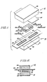
- Fig. 1 illustrates in exploded fashion a power chip package comprising component sections 10 and 12, and an exemplary power chip 14, such as a power Darlington transistor.
- Power chip 14 comprises semiconductor material, such as silicon, in a wafer-like configuration and, as illustrated with exaggerated thickness, a collector terminal 16 on its upper side and an emitter terminal 18, a first base terminal 20 and a second base terminal 22 on its lower side.
- a power diode would have only one terminal per side.
- Power chip package section 10 comprises a dielectric substrate 26 and a plurality of sheet metal leads 28, 30, and 32 attached to the upper surface of the substrate.
- Dielectric substrate 26 preferably has a thermal conductivity of at least about 2.2 watts per centimeter-degrees centigrade, such as provided by the ceramic beryllia, a preferred material.
- Dielectric substrate 26 additionally should have a thermal expansion coefficient which is close to that of power chip 14 to minimize thermally-induced expansion and contraction stresses between the two.
- chip 14 comprises silicon
- dielectric substrate 26 suitably comprises beryllia, which has a thermal expansion coefficient desirably close to that of silicon.
- Another suitable material for dielectric substrate 26 is the ceramic alumina.
- Sheet metal leads 28, 30, and 32 preferably comprise copper with a thickness in the range of from about 3 mils (0.0076cm) to 15 mils (0.038 cm), although they alternatively could comprise other, preferably high conductivity metals such as aluminum or silver.
- Sheet metal leads 28, 30, and 32 are patterned in mirror or reverse image fashion to the lower terminals 18, 20, and 22 of power chip 14 so that the terminals respectively abut sheet metal leads 28, 30, and 32 when power chip 14 is placed upon power chip carrier section 10.
- a eutectic bonding technique that is, a technique during which a molten eutectic alloy is formed between each of sheet metal leads 28, 30, and 32 and dielectric substrate 26.
- the molten eutectic alloy wets substrate 26, thereby assuring a strong bond to substrate 26.
- suitable eutectic bonding techniques are known and are discussed (and claimed) for example, in the following U.S. Patents: No. 3,766,634-G. L. Babcock et al., issued 23 October 1973 and No. 3,994,430-D. A. Cusano et al., issued 30 November 1976.
- solderable metal layer 40 preferably comprising sheet metal such as copper adhered to substrate 26 in like manner as sheet metal leads 28, 30, and 32 are adhered to substrate 26.
- Solderable layer 40 could alternatively be formed by metallizing the lower surface of substrate 26, such as through evaporation of metal onto such surface.
- Solderable layer 40 can be omitted, however, such as where power chip 14 generates only a small amount of heat, and replaced, for example, with epoxy adhesive containing metallic particles to impart a high thermal conductivity to the epoxy.
- Power chip package section 12 comprises a dielectric substrate 42, a sheet metal lead 44 attached to the lower surface of substrate 42, and a solderable metal layer 46 attached to the upper surface of substrate 42. These parts 42, 44, and 46 correspond to dielectric substrate 26, sheet metal leads 28, 30, and 32, and solderable metal layer 40, respectively, of power chip package section 10 and are selected in accordance with the criteria therefor, discussed above.
- Sheet metal lead 44 of power chip package section 12 is adapted to adjoin collector terminal 16 of power chip 14 when power chip package 10, 12 is assembled. Lead 44 does not need to be patterned, as is the case, for example, with lead 28, since collector 16 is the sole terminal of power chip 14 facing lead 44.
- the lower terminals 18, 20, and 22 of power chip 14 be solder bumped (i.e., provided with "bumps" of solder) so that they may be soldered to the respective sheet metal leads 28, 30, and 32 simply by placing power chip 14 on such leads and heating chip 14 and package section 10 to a sufficient temperature to complete a solder bond between the terminals and the leads.
- Collector terminal 16 is preferably solder coated and may be soldered to lead 44 of carrier section 12 before, during, or preferably, after the foregoing solder operation has been completed.
- Fig. 2 illustrates the cross section of a power chip package 10, 12 when assembled, with power chip 14 mounted therein, taken at line 2-2 in Fig. 1.
- Either or both solderable metal layers 40 and 46 of power chip package 10, 12 can be soldered to a single heat spreader plate or pair of plates (not shown), respectively. With either one of layers 40 or 46 soldered to a heat spreader plate, power chip 14 may be mounted collector 16 side up or collector 16 side down, as desired.
- Either or both of solderable metal layers 40 and 46 can be omitted if such layer or layers are not necessary for bonding to a heat spreader plate. For instance, both layers 40 and 46 can be omitted if package 10, 12 is otherwise bonded to a heat spreader plate, such as with an epoxy adhesive as described above.
- power chip 14 is mounted solely upon power chip package section 10 and the upper side collector terminal 16 is tinned with solder. Then, for testing, in lieu of using power chip package section 12, a broad area electrical contact (not shown) is simply pressed against collector terminal 16 of power chip 14, the sole terminal on the upper surface of power chip 14, so that precise alignment with collector terminal 16 is unnecessary.
- power chip 14 can be tested at higher levels of heat generation than in the foregoing alternative embodiment, or in presently-available power chip packages. This is because whichever one of dielectric substrates 26 and 42 is not attached to a heat spreader plate absorbs heat from power chip 14, at least transiently, to the limit of its heat capacity.
- Power chip package 10, 12 is considerably simpler in construction, and thus less costly, than currently-available power chip packages. This significantly reduces the expense of selecting power chips having similar characteristics inasmuch as power chips without desired characteristics and their packages are often discarded.
- the cruciform orientation of sheet metal leads 28 and 44 permits interconnection between the emitter and the collector of a pair of bipolar transistor power chips, each mounted in respective power chip carriers of my invention, with the remaining emitter and collector leads being spaced from each other for easy access to external circuitry (not shown).
- Sheet metal leads 28 and 44 additionally have the advantage of possessing only a low stray inductance, which reduces the possibility of undesirable voltage stresses arising therein when power chip 14 is rapidly switching large currents.
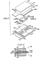
- a preferred power chip package 310, 312 is illustrated in exploded form, along with power chip 314.
- Power chip package 310,312 is similar to power chip package 10, 12 of Fig. 1, with the exception that power chip package 310, 312 includes heat transfer means for transferring heat between dielectric substrates 326 and 342.
- This heat transfer means includes projections 326a and 326b of dielectric substrate 326, which extend upwardly from the main body of dielectric substrate 326 and preferably further include solderable metal layers 350a and 350b attached to the upper surfaces of projection 326a and 326b, respectively, such as by means of a eutectic bonding technique, or by soldering to an evaporated metal layer (not shown), such as copper.
- Solderable layers 350a and 350b are adapted to abut and be soldered to sheet metal lead 344 on the underside of dielectric substrate 342 when power chip package 310, 312 is assembled.
- the heat transfer means preferably also include projections 342a and 342b, which extend downwardly from the main body of dielectric substrate 342 so as to abut solderable metal layers 352a, 352b, 352c, and 352d which are preferably attached by means of a eutectic bond to the upper surfaces of the corners of dielectric substrate 326, respectively, when power chip package 310, 312 is assembled.
- Fig. 4 is a cross-sectional view of power chip package 310, 312, fully assembled, and power chip 314, taken at line 4-4 in Fig. 3.
- Fig. 4 is a cross-sectional view of power chip package 310, 312, fully assembled, and power chip 314, taken at line 4-4 in Fig. 3.
- power chip package 310, 312 can be hermetically sealed with considerable facility, for example, by providing a heat deformable, adhesive dielectric layer, such as Silica-Seal@ 1161 sealing glass paste, on those portions of power chip package sections 310 and 312 which are to be joined together.
- a deformable adhesive layer advantageously could become cured at soldering temperatures, so as to hermetically bond together substrates 326 and 342, while power chip 314 is being soldered in place.
- a polymer sealant such as an epoxy, polyimide, or silicone, could be used to bond the dielectric substrates together.
- Power chip package 510, 512 includes a heat transfer means of different construction than the heat transfer means of power chip package 310, 312 of Fig. 3. That is, the heat transfer means of power chip package 510, 512 comprises sheet metal layers 528a and 528b on dielectric substrate 526 and complementary layer 528a' and 528b' on dielectric substrate 542. Layers 528a and 528a' are suitably formed by successively folding respective layers of metal, such as copper, which are attached to substrates 526 and 542 as with eutectic alloy compositions. Layers 528a and 528a' are preferably soldered together during assembly of power chip carrier 510, 512. Layers 528b and 528b' are suitably symmetrical in structure and form to layers 528a and 528a'.
- Fig. 6 which illustrates a cross-section of power chip package 510, 512 when assembled and power chip 514, taken at line 6-6 in Fig. 5, the pairs of sheet metal layers 528a and 528a' and 528b and 528b' are tightly compacted together and each pair extends between the upper surface of dielectric substrate 526 and the lower surface of dielectric substrate 542 so as to provide high thermal conductivity paths between these substrates.
- power chip package 510, 512 is essentially similar to power chip package 10, 12 of Fig. 1.
- the power chip package of my invention is considerably simpler in construction and thus lower in cost than currently-available power chip packages; therefore, it is much more amenable to the selection of power chips having similar characteristics.
- the embodiments of my power chip package having a pair of dielectric substrates with a power chip mounted therebetween have larger heat removal capacity than currently-available power chip packages.
- a heat transfer means provides a path or paths of high thermal conductivity between a pair of dielectric substrates having a power chip mounted therebetween, the heat removal capacity at all significant levels of heat generation in the power chip is considerably higher than in presently available power chip packages.
Description
- My invention relates to packages for semiconductor chips, and more particularly to packages incorporating high thermal conductivity elements for drawing heat away from a power semiconductor chip.
- Semiconductor chips that generate heat during operation in excess of about one watt are known in the art as "power" chips as distinct from "signal" chips, where power dissipation is usually much lower. Such heat arises primarily from 12R conduction or switching losses in the chip. To avoid thermal damage, the heat must be removed from a power chip and transferred to, for example, a metallic heat spreader plate or heat sink. However, power chips must be electrically tested at rated current in order to determine significant characteristics, such as, in a bipolar transistor, the common emitter current gain, HFE, and the collector-to-emitter voltage at device saturation, VcE (sAT). These characteristics typically vary considerably from chip to chip, even though the chips are made in the same batch. Such electrical testing requires the chip to be operated at high levels of heat generation, requiring the chip to be mounted in a package incorporating high thermal conductivity elements for removing heat from the power chip.
- A typical power chip package that is described in US-A-3 649 881 includes a high thermal conductivity dielectric substrate, such as alumina, with a single layer of solderable metal on its upper surface covering a large area of the substrate. The substrate is mounted on a metallic heat spreader plate to facilitate heat removal. That side of a power chip having only one large area electric terminal, for example, a collector terminal of a typical bipolar transistor, is positioned to face downward and is soldered to the solderable layer atop the dielectric substrate. One or more wires are then bonded to the one or more terminals on the reverse or upper side of the power chip and are connected to electrically isolated areas of the power chip that are suitable for interconnection to external circuitry.
- The presence of the bonded wire(s) on the upper side of the chip undesirably precludes a high thermal conductivity element from being attached to such upper side. Additionally, the wires bonded to the upper side of the chip are too fragile to be directly connected to testing circuitry, and therefore such wires must be first attached to rugged lead structure which, in turn, can be directly connected to testing circuitry. For high current power chips, such rugged lead structure is so large that it cannot be supported solely by the dielectric substrate on which the power chip is mounted, but must have additional mechanical support from the metallic heat spreader plate onto which the dielectric substrate is also mounted. The individual leads of the rugged lead structure must be provided with appropriate electrical insulation, so that a complete (and costly) package must be assembled before chip testing is possible. The use of such power chip packages for chip testing in order to select a group of chips with similar characteristics is especially costly, since chips with undesired characteristics along with their packages are likely to be discarded.
- An object of this invention is to provide a power chip package which is simple in construction and thus of reduced cost than presently-available power chip packages.
- A further object of the invention is to provide a power chip package capable of removing significantly more heat from a power chip than presently-available power chip packages.
- In accordance with the invention, as claimed, I provide a power chip package comprising a dielectric substrate, preferably of beryllia, and a plurality of sheet metal leads, preferably of copper, attached to a first side of the dielectric substrate, preferably by means of a eutectic bonding technique. The sheet metal leads are patterned in mirror image fashion to a plurality of terminals on one side of a power chip, for example, a power Darlington transistor. After the power chip is mounted on the sheet metal leads, as by soldering, heat generated in the power chip is drawn into the dielectric substrate via the sheet metal leads, and can be transferred to a heat sink by mounting the substrate thereon. The other side of the power chip, at least where it has one terminal, can be readily connected to external circuitry for testing simply by pressing a large area conductor against the exposed terminal. In addition to the power chip package thus far described, a second dielectric substrate having a sheet metal lead attached thereto is included. This lead is adapted to be connected to a single, large area terminal of the power chip. This power chip package provides even more heat removal capacity than presently-available power chip packages, since the second dielectric substrate absorbs heat from the power chip. Further heat transfer means are provided for transferring heat from the second dielectric substrate to the first one. The heat transfer means may comprise, for example, projections of one dielectric substrate which abut the other substrate when the package is assembled. This power chip package is capable of removing significantly more heat from a power chip than presently-available power chip packages, because heat removed from both sides of the power chip by the pair of substrates can be transferred to a heat sink.
- While this specification concludes with claims particularly pointing out and distinctly claiming the subject matter which I regard as my invention, it is believed that the invention, along with further objects and advantages thereof, will be better understood from the following description, when considered with the following figures of the drawings, in which like parts have like reference numerals:
- Fig. 1 is an exploded view of a power chip package, along with a power chip;
- Fig. 2 is a cross-sectional view of the power chip package of Fig. 1 when assembled, taken along line 2-2 of Fig. 1;
- Fig. 3 is a view similar to Fig. 1 illustrating a power chip package in a further embodiment;
- Fig. 4 is a cross-sectional view of the power chip package of Fig. 3 when assembled, taken along line 4-4 in Fig. 3;
- Fig. 5 is a view also similar to Fig. 1, illustrating a power chip package in accordance with my invention; and
- Fig. 6 is a cross-sectional view of the power chip package of Fig. 5 when assembled, taken along line 6-6 in Fig. 5.
- Fig. 1 illustrates in exploded fashion a power chip package comprising
component sections 10 and 12, and an exemplary power chip 14, such as a power Darlington transistor. Power chip 14 comprises semiconductor material, such as silicon, in a wafer-like configuration and, as illustrated with exaggerated thickness, acollector terminal 16 on its upper side and an emitter terminal 18, a first base terminal 20 and asecond base terminal 22 on its lower side. By comparison, a power diode would have only one terminal per side. - Power
chip package section 10 comprises adielectric substrate 26 and a plurality of sheet metal leads 28, 30, and 32 attached to the upper surface of the substrate.Dielectric substrate 26 preferably has a thermal conductivity of at least about 2.2 watts per centimeter-degrees centigrade, such as provided by the ceramic beryllia, a preferred material.Dielectric substrate 26 additionally should have a thermal expansion coefficient which is close to that of power chip 14 to minimize thermally-induced expansion and contraction stresses between the two. Where chip 14 comprises silicon,dielectric substrate 26 suitably comprises beryllia, which has a thermal expansion coefficient desirably close to that of silicon. Another suitable material fordielectric substrate 26 is the ceramic alumina. - Sheet metal leads 28, 30, and 32 preferably comprise copper with a thickness in the range of from about 3 mils (0.0076cm) to 15 mils (0.038 cm), although they alternatively could comprise other, preferably high conductivity metals such as aluminum or silver. Sheet metal leads 28, 30, and 32 are patterned in mirror or reverse image fashion to the
lower terminals 18, 20, and 22 of power chip 14 so that the terminals respectively abut sheet metal leads 28, 30, and 32 when power chip 14 is placed upon powerchip carrier section 10. - I prefer to attach sheet metal leads 28, 30, and 32 to
dielectric substrate 26 by means of a eutectic bonding technique; that is, a technique during which a molten eutectic alloy is formed between each of sheet metal leads 28, 30, and 32 anddielectric substrate 26. The molten eutecticalloy wets substrate 26, thereby assuring a strong bond tosubstrate 26. Details of suitable eutectic bonding techniques are known and are discussed (and claimed) for example, in the following U.S. Patents: No. 3,766,634-G. L. Babcock et al., issued 23 October 1973 and No. 3,994,430-D. A. Cusano et al., issued 30 November 1976. These patents are assigned to the assignee of this invention and their disclosures concerning the eutectic bonding technique are incorporated herein by reference. As an alternative to using a eutectic bonding technique for attaching sheet metal leads 28, 30, and 32 todielectric substrate 26, the upper surface ofdielectric substrate 26 could be metallized with a solderable metal (not shown), such as by evaporation of copper onto such surface, and then sheet metal leads 28, 30, and 32 soldered to the solderable metal layer. This alternative requires that the solderable metal layer be patterned so as not to electrically short together the various sheet metal leads 28,30, and 32. Such patterning is suitably accomplished using conventional photolithographic masking techniques while the solderable metal layer is being formed on the upper surface ofdielectric substrate 26. - I prefer that the underside of
dielectric substrate 26 be provided with a solderable metal layer 40, preferably comprising sheet metal such as copper adhered tosubstrate 26 in like manner as sheet metal leads 28, 30, and 32 are adhered tosubstrate 26. Solderable layer 40 could alternatively be formed by metallizing the lower surface ofsubstrate 26, such as through evaporation of metal onto such surface. Solderable layer 40 can be omitted, however, such as where power chip 14 generates only a small amount of heat, and replaced, for example, with epoxy adhesive containing metallic particles to impart a high thermal conductivity to the epoxy. - Power chip package section 12 comprises a
dielectric substrate 42, asheet metal lead 44 attached to the lower surface ofsubstrate 42, and asolderable metal layer 46 attached to the upper surface ofsubstrate 42. Theseparts dielectric substrate 26, sheet metal leads 28, 30, and 32, and solderable metal layer 40, respectively, of powerchip package section 10 and are selected in accordance with the criteria therefor, discussed above. -
Sheet metal lead 44 of power chip package section 12 is adapted toadjoin collector terminal 16 of power chip 14 whenpower chip package 10, 12 is assembled.Lead 44 does not need to be patterned, as is the case, for example, with lead 28, sincecollector 16 is the sole terminal of power chip 14 facinglead 44. - In mounting power chip 14 within
power chip package 10, 12, it is preferable that thelower terminals 18, 20, and 22 of power chip 14 be solder bumped (i.e., provided with "bumps" of solder) so that they may be soldered to the respective sheet metal leads 28, 30, and 32 simply by placing power chip 14 on such leads and heating chip 14 andpackage section 10 to a sufficient temperature to complete a solder bond between the terminals and the leads.Collector terminal 16 is preferably solder coated and may be soldered to lead 44 of carrier section 12 before, during, or preferably, after the foregoing solder operation has been completed. - Fig. 2 illustrates the cross section of a
power chip package 10, 12 when assembled, with power chip 14 mounted therein, taken at line 2-2 in Fig. 1. Either or both solderable metal layers 40 and 46 ofpower chip package 10, 12 can be soldered to a single heat spreader plate or pair of plates (not shown), respectively. With either one oflayers 40 or 46 soldered to a heat spreader plate, power chip 14 may be mountedcollector 16 side up orcollector 16 side down, as desired. Either or both of solderable metal layers 40 and 46 can be omitted if such layer or layers are not necessary for bonding to a heat spreader plate. For instance, bothlayers 40 and 46 can be omitted ifpackage 10, 12 is otherwise bonded to a heat spreader plate, such as with an epoxy adhesive as described above. - In an alternative embodiment power chip 14 is mounted solely upon power
chip package section 10 and the upperside collector terminal 16 is tinned with solder. Then, for testing, in lieu of using power chip package section 12, a broad area electrical contact (not shown) is simply pressed againstcollector terminal 16 of power chip 14, the sole terminal on the upper surface of power chip 14, so that precise alignment withcollector terminal 16 is unnecessary. In suchembodiment dielectric substrate 26, selected for its high thermal conductivity, readily draws away heat from power chip 14 while chip 14 is undergoing electrical testing. - Considering again the Fig. 2 embodiment including power chip package section 12, as illustrated, power chip 14 can be tested at higher levels of heat generation than in the foregoing alternative embodiment, or in presently-available power chip packages. This is because whichever one of
dielectric substrates -
Power chip package 10, 12 is considerably simpler in construction, and thus less costly, than currently-available power chip packages. This significantly reduces the expense of selecting power chips having similar characteristics inasmuch as power chips without desired characteristics and their packages are often discarded. Advantageously, the cruciform orientation of sheet metal leads 28 and 44 permits interconnection between the emitter and the collector of a pair of bipolar transistor power chips, each mounted in respective power chip carriers of my invention, with the remaining emitter and collector leads being spaced from each other for easy access to external circuitry (not shown). Sheet metal leads 28 and 44 additionally have the advantage of possessing only a low stray inductance, which reduces the possibility of undesirable voltage stresses arising therein when power chip 14 is rapidly switching large currents. - Turning to Fig. 3, a preferred
power chip package power chip 314. Power chip package 310,312 is similar topower chip package 10, 12 of Fig. 1, with the exception thatpower chip package dielectric substrates projections dielectric substrate 326, which extend upwardly from the main body ofdielectric substrate 326 and preferably further includesolderable metal layers 350a and 350b attached to the upper surfaces ofprojection Solderable layers 350a and 350b are adapted to abut and be soldered tosheet metal lead 344 on the underside ofdielectric substrate 342 whenpower chip package projections dielectric substrate 342 so as to abutsolderable metal layers dielectric substrate 326, respectively, whenpower chip package projections power chip package chip 314 whenpower chip package projection 326b. - The advantages of including the foregoing heat transfer means between
dielectric substrates power chip package power chip 314, taken at line 4-4 in Fig. 3. With heat from one ofdielectric substrates power chip package power chip 314, is considerably enhanced over currently-available power chip packages. Advantageously,power chip package chip package sections substrates power chip 314 is being soldered in place. Alternatively, a polymer sealant, such as an epoxy, polyimide, or silicone, could be used to bond the dielectric substrates together. - Referring now to Fig. 5, a
power chip package power chip 514, is illustrated in exploded form.Power chip package power chip package power chip package sheet metal layers dielectric substrate 526 andcomplementary layer 528a' and 528b' ondielectric substrate 542.Layers substrates Layers power chip carrier Layers layers - As best shown in Fig. 6, which illustrates a cross-section of
power chip package power chip 514, taken at line 6-6 in Fig. 5, the pairs ofsheet metal layers dielectric substrate 526 and the lower surface ofdielectric substrate 542 so as to provide high thermal conductivity paths between these substrates. Apart from the different configurations and orientations of sheet metal leads 528, 530, 532 and 544,power chip package power chip package 10, 12 of Fig. 1. - In summary, the power chip package of my invention is considerably simpler in construction and thus lower in cost than currently-available power chip packages; therefore, it is much more amenable to the selection of power chips having similar characteristics. The embodiments of my power chip package having a pair of dielectric substrates with a power chip mounted therebetween have larger heat removal capacity than currently-available power chip packages. In the preferred embodiments of my invention in which a heat transfer means provides a path or paths of high thermal conductivity between a pair of dielectric substrates having a power chip mounted therebetween, the heat removal capacity at all significant levels of heat generation in the power chip is considerably higher than in presently available power chip packages.
Claims (15)
Applications Claiming Priority (2)
| Application Number | Priority Date | Filing Date | Title |
|---|---|---|---|
| US06/455,186 US4538170A (en) | 1983-01-03 | 1983-01-03 | Power chip package |
| US455186 | 1983-01-03 |
Publications (3)
| Publication Number | Publication Date |
|---|---|
| EP0115000A2 EP0115000A2 (en) | 1984-08-08 |
| EP0115000A3 EP0115000A3 (en) | 1986-11-26 |
| EP0115000B1 true EP0115000B1 (en) | 1989-08-09 |
Family
ID=23807740
Family Applications (1)
| Application Number | Title | Priority Date | Filing Date |
|---|---|---|---|
| EP83112678A Expired EP0115000B1 (en) | 1983-01-03 | 1983-12-16 | Power chip package |
Country Status (5)
| Country | Link |
|---|---|
| US (1) | US4538170A (en) |
| EP (1) | EP0115000B1 (en) |
| JP (1) | JPS59141249A (en) |
| DE (1) | DE3380380D1 (en) |
| IE (1) | IE55369B1 (en) |
Cited By (1)
| Publication number | Priority date | Publication date | Assignee | Title |
|---|---|---|---|---|
| US11251112B2 (en) | 2018-12-05 | 2022-02-15 | Hyundai Mobis Co., Ltd. | Dual side cooling power module and manufacturing method of the same |
Families Citing this family (29)
| Publication number | Priority date | Publication date | Assignee | Title |
|---|---|---|---|---|
| US4646129A (en) * | 1983-09-06 | 1987-02-24 | General Electric Company | Hermetic power chip packages |
| KR900001273B1 (en) * | 1983-12-23 | 1990-03-05 | 후지쑤 가부시끼가이샤 | Semiconductor integrated circuit device |
| DE3406528A1 (en) * | 1984-02-23 | 1985-08-29 | Brown, Boveri & Cie Ag, 6800 Mannheim | PERFORMANCE SEMICONDUCTOR MODULE |
| JPS60239051A (en) * | 1984-05-11 | 1985-11-27 | Mitsubishi Electric Corp | Semiconductor device |
| US4716124A (en) * | 1984-06-04 | 1987-12-29 | General Electric Company | Tape automated manufacture of power semiconductor devices |
| US4635092A (en) * | 1984-06-04 | 1987-01-06 | General Electric Company | Tape automated manufacture of power semiconductor devices |
| US4931906A (en) * | 1988-03-25 | 1990-06-05 | Unitrode Corporation | Hermetically sealed, surface mountable component and carrier for semiconductor devices |
| US5139972A (en) * | 1991-02-28 | 1992-08-18 | General Electric Company | Batch assembly of high density hermetic packages for power semiconductor chips |
| FR2673765A1 (en) * | 1991-03-05 | 1992-09-11 | Thomson Composants Militaires | INTEGRATED CIRCUIT BOX WITH POWER CONNECTION. |
| US5777259A (en) * | 1994-01-14 | 1998-07-07 | Brush Wellman Inc. | Heat exchanger assembly and method for making the same |
| CA2140311A1 (en) * | 1994-01-14 | 1995-07-15 | Joseph P. Mennucci | Multilayer laminate product and process |
| US5539254A (en) * | 1994-03-09 | 1996-07-23 | Delco Electronics Corp. | Substrate subassembly for a transistor switch module |
| US6022426A (en) * | 1995-05-31 | 2000-02-08 | Brush Wellman Inc. | Multilayer laminate process |
| DE19751423A1 (en) * | 1997-11-20 | 1999-06-02 | Bosch Gmbh Robert | Window heating |
| US5895974A (en) * | 1998-04-06 | 1999-04-20 | Delco Electronics Corp. | Durable substrate subassembly for transistor switch module |
| US6127727A (en) * | 1998-04-06 | 2000-10-03 | Delco Electronics Corp. | Semiconductor substrate subassembly with alignment and stress relief features |
| JP2000091485A (en) | 1998-07-14 | 2000-03-31 | Denso Corp | Semiconductor device |
| US6072240A (en) * | 1998-10-16 | 2000-06-06 | Denso Corporation | Semiconductor chip package |
| US6194246B1 (en) | 1999-08-25 | 2001-02-27 | Motorola Inc. | Process for fabricating electronic devices having a thermally conductive substrate |
| US6703707B1 (en) * | 1999-11-24 | 2004-03-09 | Denso Corporation | Semiconductor device having radiation structure |
| US6693350B2 (en) | 1999-11-24 | 2004-02-17 | Denso Corporation | Semiconductor device having radiation structure and method for manufacturing semiconductor device having radiation structure |
| JP4479121B2 (en) * | 2001-04-25 | 2010-06-09 | 株式会社デンソー | Manufacturing method of semiconductor device |
| TW591363B (en) * | 2001-10-10 | 2004-06-11 | Aavid Thermalloy Llc | Heat collector with mounting plate |
| US6812553B2 (en) * | 2002-01-16 | 2004-11-02 | Delphi Technologies, Inc. | Electrically isolated and thermally conductive double-sided pre-packaged component |
| EP2216891B1 (en) * | 2003-08-21 | 2012-01-04 | Denso Corporation | Mounting structure ofa semiconductor device |
| US7229855B2 (en) * | 2005-02-23 | 2007-06-12 | Delphi Technologies, Inc. | Process for assembling a double-sided circuit component |
| US8124449B2 (en) | 2008-12-02 | 2012-02-28 | Infineon Technologies Ag | Device including a semiconductor chip and metal foils |
| TWM460508U (en) * | 2013-03-04 | 2013-08-21 | Giant Technology Co Ltd | Heat-dissipating structure of electrical shielding cover |
| US11018425B1 (en) * | 2015-05-01 | 2021-05-25 | Rockwell Collins, Inc. | Active electronically scanned array with power amplifier drain bias tapering for optimal power added efficiency |
Family Cites Families (15)
| Publication number | Priority date | Publication date | Assignee | Title |
|---|---|---|---|---|
| US29325A (en) * | 1860-07-24 | Improvement in mowing-machines | ||
| US3025436A (en) * | 1959-08-19 | 1962-03-13 | Itt | High current rectifier |
| US3196325A (en) * | 1960-02-16 | 1965-07-20 | Microwave Ass | Electrode connection to mesa type semiconductor device |
| NL283717A (en) * | 1961-11-28 | |||
| DE1212638C2 (en) * | 1963-02-23 | 1966-09-29 | Licentia Gmbh | Semiconductor arrangement with a semiconductor element enclosed in a housing |
| CH448213A (en) * | 1966-03-16 | 1967-12-15 | Secheron Atel | AC semiconductor control device |
| GB1210584A (en) * | 1967-07-07 | 1970-10-28 | Hitachi Ltd | Semiconductor device and method of manufacturing the same |
| US3566212A (en) * | 1969-02-24 | 1971-02-23 | Trw Semiconductors Inc | High temperature semiconductor package |
| US3569798A (en) * | 1969-05-13 | 1971-03-09 | Rca Corp | Double heat sink semiconductor device |
| US3611059A (en) * | 1970-06-11 | 1971-10-05 | Rca Corp | Transistor assembly |
| US3649881A (en) * | 1970-08-31 | 1972-03-14 | Rca Corp | High-power semiconductor device assembly |
| US3766634A (en) * | 1972-04-20 | 1973-10-23 | Gen Electric | Method of direct bonding metals to non-metallic substrates |
| US3842189A (en) * | 1973-01-08 | 1974-10-15 | Rca Corp | Contact array and method of making the same |
| US3994430A (en) * | 1975-07-30 | 1976-11-30 | General Electric Company | Direct bonding of metals to ceramics and metals |
| US4067041A (en) * | 1975-09-29 | 1978-01-03 | Hutson Jearld L | Semiconductor device package and method of making same |
-
1983
- 1983-01-03 US US06/455,186 patent/US4538170A/en not_active Expired - Lifetime
- 1983-11-16 IE IE2686/83A patent/IE55369B1/en not_active IP Right Cessation
- 1983-12-16 EP EP83112678A patent/EP0115000B1/en not_active Expired
- 1983-12-16 DE DE8383112678T patent/DE3380380D1/en not_active Expired
- 1983-12-28 JP JP58245641A patent/JPS59141249A/en active Granted
Cited By (3)
| Publication number | Priority date | Publication date | Assignee | Title |
|---|---|---|---|---|
| US11251112B2 (en) | 2018-12-05 | 2022-02-15 | Hyundai Mobis Co., Ltd. | Dual side cooling power module and manufacturing method of the same |
| DE102019132837B4 (en) | 2018-12-05 | 2022-06-15 | Hyundai Mobis Co., Ltd. | Double-sided cooling power module and method for its manufacture |
| US11862542B2 (en) | 2018-12-05 | 2024-01-02 | Hyundai Mobis Co., Ltd. | Dual side cooling power module and manufacturing method of the same |
Also Published As
| Publication number | Publication date |
|---|---|
| IE832686L (en) | 1984-07-03 |
| US4538170A (en) | 1985-08-27 |
| EP0115000A3 (en) | 1986-11-26 |
| DE3380380D1 (en) | 1989-09-14 |
| JPH0129068B2 (en) | 1989-06-07 |
| JPS59141249A (en) | 1984-08-13 |
| EP0115000A2 (en) | 1984-08-08 |
| IE55369B1 (en) | 1990-08-29 |
Similar Documents
| Publication | Publication Date | Title |
|---|---|---|
| EP0115000B1 (en) | Power chip package | |
| US4907067A (en) | Thermally efficient power device package | |
| US4556899A (en) | Insulated type semiconductor devices | |
| US6731002B2 (en) | High frequency power device with a plastic molded package and direct bonded substrate | |
| US5650662A (en) | Direct bonded heat spreader | |
| US4700273A (en) | Circuit assembly with semiconductor expansion matched thermal path | |
| US4266090A (en) | All metal flat package | |
| US7132356B1 (en) | Interconnection method | |
| JPH05259328A (en) | Semiconductor module | |
| JPS6128219B2 (en) | ||
| EP0741411B1 (en) | Method of fabricating multi-chip packages | |
| US5406120A (en) | Hermetically sealed semiconductor ceramic package | |
| EP0650193A2 (en) | Semiconductor device and method for manufacturing the same | |
| GB2194477A (en) | Solder joint | |
| JPH0118583B2 (en) | ||
| JP2003224234A (en) | Semiconductor device | |
| US6225700B1 (en) | Package for a semiconductor element having depressions containing solder terminals | |
| JPH07176664A (en) | Semiconductor device and fabrication thereof | |
| EP0525651B1 (en) | Package structure for one or more IC chips | |
| JPH08148647A (en) | Semiconductor device | |
| US6291893B1 (en) | Power semiconductor device for “flip-chip” connections | |
| GB2165704A (en) | Heat dissipation for electronic components | |
| JP3048707B2 (en) | Hybrid integrated circuit | |
| US5313091A (en) | Package for a high power electrical component | |
| JP2800605B2 (en) | Semiconductor device |
Legal Events
| Date | Code | Title | Description |
|---|---|---|---|
| PUAI | Public reference made under article 153(3) epc to a published international application that has entered the european phase |
Free format text: ORIGINAL CODE: 0009012 |
|
| AK | Designated contracting states |
Designated state(s): DE FR GB NL SE |
|
| 17P | Request for examination filed |
Effective date: 19841106 |
|
| PUAL | Search report despatched |
Free format text: ORIGINAL CODE: 0009013 |
|
| AK | Designated contracting states |
Kind code of ref document: A3 Designated state(s): DE FR GB NL SE |
|
| 17Q | First examination report despatched |
Effective date: 19870825 |
|
| GRAA | (expected) grant |
Free format text: ORIGINAL CODE: 0009210 |
|
| AK | Designated contracting states |
Kind code of ref document: B1 Designated state(s): DE FR GB NL SE |
|
| REF | Corresponds to: |
Ref document number: 3380380 Country of ref document: DE Date of ref document: 19890914 |
|
| ET | Fr: translation filed | ||
| PLBE | No opposition filed within time limit |
Free format text: ORIGINAL CODE: 0009261 |
|
| STAA | Information on the status of an ep patent application or granted ep patent |
Free format text: STATUS: NO OPPOSITION FILED WITHIN TIME LIMIT |
|
| 26N | No opposition filed | ||
| EAL | Se: european patent in force in sweden |
Ref document number: 83112678.4 |
|
| PGFP | Annual fee paid to national office [announced via postgrant information from national office to epo] |
Ref country code: SE Payment date: 19991202 Year of fee payment: 17 Ref country code: DE Payment date: 19991202 Year of fee payment: 17 |
|
| PGFP | Annual fee paid to national office [announced via postgrant information from national office to epo] |
Ref country code: GB Payment date: 19991203 Year of fee payment: 17 Ref country code: FR Payment date: 19991203 Year of fee payment: 17 |
|
| PGFP | Annual fee paid to national office [announced via postgrant information from national office to epo] |
Ref country code: NL Payment date: 19991213 Year of fee payment: 17 |
|
| PG25 | Lapsed in a contracting state [announced via postgrant information from national office to epo] |
Ref country code: GB Free format text: LAPSE BECAUSE OF NON-PAYMENT OF DUE FEES Effective date: 20001216 |
|
| PG25 | Lapsed in a contracting state [announced via postgrant information from national office to epo] |
Ref country code: SE Free format text: LAPSE BECAUSE OF NON-PAYMENT OF DUE FEES Effective date: 20001217 |
|
| PG25 | Lapsed in a contracting state [announced via postgrant information from national office to epo] |
Ref country code: NL Free format text: LAPSE BECAUSE OF NON-PAYMENT OF DUE FEES Effective date: 20010701 |
|
| GBPC | Gb: european patent ceased through non-payment of renewal fee |
Effective date: 20001216 |
|
| EUG | Se: european patent has lapsed |
Ref document number: 83112678.4 |
|
| PG25 | Lapsed in a contracting state [announced via postgrant information from national office to epo] |
Ref country code: FR Free format text: LAPSE BECAUSE OF NON-PAYMENT OF DUE FEES Effective date: 20010831 |
|
| NLV4 | Nl: lapsed or anulled due to non-payment of the annual fee |
Effective date: 20010701 |
|
| REG | Reference to a national code |
Ref country code: FR Ref legal event code: ST |
|
| PG25 | Lapsed in a contracting state [announced via postgrant information from national office to epo] |
Ref country code: DE Free format text: LAPSE BECAUSE OF NON-PAYMENT OF DUE FEES Effective date: 20011002 |