EP0114211B1 - Multi-layer flexible film module - Google Patents
Multi-layer flexible film module Download PDFInfo
- Publication number
- EP0114211B1 EP0114211B1 EP83110965A EP83110965A EP0114211B1 EP 0114211 B1 EP0114211 B1 EP 0114211B1 EP 83110965 A EP83110965 A EP 83110965A EP 83110965 A EP83110965 A EP 83110965A EP 0114211 B1 EP0114211 B1 EP 0114211B1
- Authority
- EP
- European Patent Office
- Prior art keywords
- circuitry
- layer
- polyimide
- chrome
- substrate
- Prior art date
- Legal status (The legal status is an assumption and is not a legal conclusion. Google has not performed a legal analysis and makes no representation as to the accuracy of the status listed.)
- Expired
Links
Images
Classifications
-
- H—ELECTRICITY
- H10—SEMICONDUCTOR DEVICES; ELECTRIC SOLID-STATE DEVICES NOT OTHERWISE PROVIDED FOR
- H10W—GENERIC PACKAGES, INTERCONNECTIONS, CONNECTORS OR OTHER CONSTRUCTIONAL DETAILS OF DEVICES COVERED BY CLASS H10
- H10W70/00—Package substrates; Interposers; Redistribution layers [RDL]
- H10W70/01—Manufacture or treatment
- H10W70/05—Manufacture or treatment of insulating or insulated package substrates, or of interposers, or of redistribution layers
-
- H—ELECTRICITY
- H05—ELECTRIC TECHNIQUES NOT OTHERWISE PROVIDED FOR
- H05K—PRINTED CIRCUITS; CASINGS OR CONSTRUCTIONAL DETAILS OF ELECTRIC APPARATUS; MANUFACTURE OF ASSEMBLAGES OF ELECTRICAL COMPONENTS
- H05K3/00—Apparatus or processes for manufacturing printed circuits
- H05K3/10—Apparatus or processes for manufacturing printed circuits in which conductive material is applied to the insulating support in such a manner as to form the desired conductive pattern
- H05K3/20—Apparatus or processes for manufacturing printed circuits in which conductive material is applied to the insulating support in such a manner as to form the desired conductive pattern by affixing prefabricated conductor pattern
-
- H—ELECTRICITY
- H05—ELECTRIC TECHNIQUES NOT OTHERWISE PROVIDED FOR
- H05K—PRINTED CIRCUITS; CASINGS OR CONSTRUCTIONAL DETAILS OF ELECTRIC APPARATUS; MANUFACTURE OF ASSEMBLAGES OF ELECTRICAL COMPONENTS
- H05K3/00—Apparatus or processes for manufacturing printed circuits
- H05K3/46—Manufacturing multilayer circuits
- H05K3/4644—Manufacturing multilayer circuits by building the multilayer layer by layer, i.e. build-up multilayer circuits
- H05K3/467—Adding a circuit layer by thin film methods
-
- H—ELECTRICITY
- H10—SEMICONDUCTOR DEVICES; ELECTRIC SOLID-STATE DEVICES NOT OTHERWISE PROVIDED FOR
- H10W—GENERIC PACKAGES, INTERCONNECTIONS, CONNECTORS OR OTHER CONSTRUCTIONAL DETAILS OF DEVICES COVERED BY CLASS H10
- H10W70/00—Package substrates; Interposers; Redistribution layers [RDL]
- H10W70/60—Insulating or insulated package substrates; Interposers; Redistribution layers
- H10W70/611—Insulating or insulated package substrates; Interposers; Redistribution layers for connecting multiple chips together
-
- H—ELECTRICITY
- H10—SEMICONDUCTOR DEVICES; ELECTRIC SOLID-STATE DEVICES NOT OTHERWISE PROVIDED FOR
- H10W—GENERIC PACKAGES, INTERCONNECTIONS, CONNECTORS OR OTHER CONSTRUCTIONAL DETAILS OF DEVICES COVERED BY CLASS H10
- H10W70/00—Package substrates; Interposers; Redistribution layers [RDL]
- H10W70/60—Insulating or insulated package substrates; Interposers; Redistribution layers
- H10W70/62—Insulating or insulated package substrates; Interposers; Redistribution layers characterised by their interconnections
- H10W70/63—Vias, e.g. via plugs
- H10W70/635—Through-vias
-
- H—ELECTRICITY
- H10—SEMICONDUCTOR DEVICES; ELECTRIC SOLID-STATE DEVICES NOT OTHERWISE PROVIDED FOR
- H10W—GENERIC PACKAGES, INTERCONNECTIONS, CONNECTORS OR OTHER CONSTRUCTIONAL DETAILS OF DEVICES COVERED BY CLASS H10
- H10W70/00—Package substrates; Interposers; Redistribution layers [RDL]
- H10W70/60—Insulating or insulated package substrates; Interposers; Redistribution layers
- H10W70/67—Insulating or insulated package substrates; Interposers; Redistribution layers characterised by their insulating layers or insulating parts
- H10W70/69—Insulating materials thereof
- H10W70/695—Organic materials
-
- H—ELECTRICITY
- H05—ELECTRIC TECHNIQUES NOT OTHERWISE PROVIDED FOR
- H05K—PRINTED CIRCUITS; CASINGS OR CONSTRUCTIONAL DETAILS OF ELECTRIC APPARATUS; MANUFACTURE OF ASSEMBLAGES OF ELECTRICAL COMPONENTS
- H05K1/00—Printed circuits
- H05K1/02—Details
- H05K1/03—Use of materials for the substrate
- H05K1/0393—Flexible materials
-
- H—ELECTRICITY
- H05—ELECTRIC TECHNIQUES NOT OTHERWISE PROVIDED FOR
- H05K—PRINTED CIRCUITS; CASINGS OR CONSTRUCTIONAL DETAILS OF ELECTRIC APPARATUS; MANUFACTURE OF ASSEMBLAGES OF ELECTRICAL COMPONENTS
- H05K2201/00—Indexing scheme relating to printed circuits covered by H05K1/00
- H05K2201/01—Dielectrics
- H05K2201/0137—Materials
- H05K2201/0154—Polyimide
-
- H—ELECTRICITY
- H05—ELECTRIC TECHNIQUES NOT OTHERWISE PROVIDED FOR
- H05K—PRINTED CIRCUITS; CASINGS OR CONSTRUCTIONAL DETAILS OF ELECTRIC APPARATUS; MANUFACTURE OF ASSEMBLAGES OF ELECTRICAL COMPONENTS
- H05K2201/00—Indexing scheme relating to printed circuits covered by H05K1/00
- H05K2201/03—Conductive materials
- H05K2201/0302—Properties and characteristics in general
- H05K2201/0317—Thin film conductor layer; Thin film passive component
-
- H—ELECTRICITY
- H05—ELECTRIC TECHNIQUES NOT OTHERWISE PROVIDED FOR
- H05K—PRINTED CIRCUITS; CASINGS OR CONSTRUCTIONAL DETAILS OF ELECTRIC APPARATUS; MANUFACTURE OF ASSEMBLAGES OF ELECTRICAL COMPONENTS
- H05K2203/00—Indexing scheme relating to apparatus or processes for manufacturing printed circuits covered by H05K3/00
- H05K2203/01—Tools for processing; Objects used during processing
- H05K2203/0147—Carriers and holders
- H05K2203/0152—Temporary metallic carrier, e.g. for transferring material
-
- H—ELECTRICITY
- H05—ELECTRIC TECHNIQUES NOT OTHERWISE PROVIDED FOR
- H05K—PRINTED CIRCUITS; CASINGS OR CONSTRUCTIONAL DETAILS OF ELECTRIC APPARATUS; MANUFACTURE OF ASSEMBLAGES OF ELECTRICAL COMPONENTS
- H05K2203/00—Indexing scheme relating to apparatus or processes for manufacturing printed circuits covered by H05K3/00
- H05K2203/03—Metal processing
- H05K2203/0376—Etching temporary metallic carrier substrate
-
- H—ELECTRICITY
- H05—ELECTRIC TECHNIQUES NOT OTHERWISE PROVIDED FOR
- H05K—PRINTED CIRCUITS; CASINGS OR CONSTRUCTIONAL DETAILS OF ELECTRIC APPARATUS; MANUFACTURE OF ASSEMBLAGES OF ELECTRICAL COMPONENTS
- H05K2203/00—Indexing scheme relating to apparatus or processes for manufacturing printed circuits covered by H05K3/00
- H05K2203/07—Treatments involving liquids, e.g. plating, rinsing
- H05K2203/0703—Plating
- H05K2203/0723—Electroplating, e.g. finish plating
-
- H—ELECTRICITY
- H05—ELECTRIC TECHNIQUES NOT OTHERWISE PROVIDED FOR
- H05K—PRINTED CIRCUITS; CASINGS OR CONSTRUCTIONAL DETAILS OF ELECTRIC APPARATUS; MANUFACTURE OF ASSEMBLAGES OF ELECTRICAL COMPONENTS
- H05K3/00—Apparatus or processes for manufacturing printed circuits
- H05K3/0011—Working of insulating substrates or insulating layers
- H05K3/0017—Etching of the substrate by chemical or physical means
- H05K3/002—Etching of the substrate by chemical or physical means by liquid chemical etching
-
- H—ELECTRICITY
- H05—ELECTRIC TECHNIQUES NOT OTHERWISE PROVIDED FOR
- H05K—PRINTED CIRCUITS; CASINGS OR CONSTRUCTIONAL DETAILS OF ELECTRIC APPARATUS; MANUFACTURE OF ASSEMBLAGES OF ELECTRICAL COMPONENTS
- H05K3/00—Apparatus or processes for manufacturing printed circuits
- H05K3/38—Improvement of the adhesion between the insulating substrate and the metal
- H05K3/388—Improvement of the adhesion between the insulating substrate and the metal by the use of a metallic or inorganic thin film adhesion layer
-
- H—ELECTRICITY
- H10—SEMICONDUCTOR DEVICES; ELECTRIC SOLID-STATE DEVICES NOT OTHERWISE PROVIDED FOR
- H10W—GENERIC PACKAGES, INTERCONNECTIONS, CONNECTORS OR OTHER CONSTRUCTIONAL DETAILS OF DEVICES COVERED BY CLASS H10
- H10W90/00—Package configurations
- H10W90/701—Package configurations characterised by the relative positions of pads or connectors relative to package parts
- H10W90/721—Package configurations characterised by the relative positions of pads or connectors relative to package parts of bump connectors
- H10W90/724—Package configurations characterised by the relative positions of pads or connectors relative to package parts of bump connectors between a chip and a stacked insulating package substrate, interposer or RDL
-
- Y—GENERAL TAGGING OF NEW TECHNOLOGICAL DEVELOPMENTS; GENERAL TAGGING OF CROSS-SECTIONAL TECHNOLOGIES SPANNING OVER SEVERAL SECTIONS OF THE IPC; TECHNICAL SUBJECTS COVERED BY FORMER USPC CROSS-REFERENCE ART COLLECTIONS [XRACs] AND DIGESTS
- Y10—TECHNICAL SUBJECTS COVERED BY FORMER USPC
- Y10T—TECHNICAL SUBJECTS COVERED BY FORMER US CLASSIFICATION
- Y10T29/00—Metal working
- Y10T29/49—Method of mechanical manufacture
- Y10T29/49002—Electrical device making
- Y10T29/49117—Conductor or circuit manufacturing
- Y10T29/49124—On flat or curved insulated base, e.g., printed circuit, etc.
- Y10T29/49155—Manufacturing circuit on or in base
Definitions
- This invention relates to electronic packaging and more particularly to high density, low cost packaging of electronic circuitry.
- the prior art also teaches various techniques for avoiding problems caused by thermal mismatch between integrated circuit chips and the support on which the chips are mounted.
- One known technique for avoiding problems due to thermal mismatch is to mount the chip on a flexible film carrier.
- U.S. Patent 4 231 154 shows an integrated circuit chip mounted on a very thin layer of circuitized polyimide.
- Double sided circuitry is also well known.
- Such circuitry generally includes a carrier with circuitry on both sides of the carrier.
- the circuitry on the two sides of the carrier is generally interconnected by vias or through holes.
- the carrier in such circuitry is generally a material such as epoxy glass which can be etched or drilled to provide passages for the via interconnections.
- Another object of this invention is to provide a method of manufacturing the assembly described above utilizing a temporary support member.
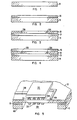
- the polyimide with circuitry on both of its surfaces is fabricated by depositing a first layer of conventional chrome-copper-chrome circuitry on an aluminum carrier. This first layer of circuitry is covered with polyimide. Vias are etched into the polyimide and then the polyimide is fully cured. A second layer of conventional circuitry is deposited on the top surface of the polyimide. The aluminum carrier is then etched away using hydrochloric acid.
- the result is a thin film having circuitry on both of its surfaces.
- the two layers of circuitry are interconnected by means of etched vias.
- the aluminium can be etched away without damaging the circuitry since hydrochloric acid attacks aluminum but it does not attack chrome.
- circuitry 20 is deposited on top of the aluminum carrier as shown in Figure 2.
- Circuitry 20 can be evaporated, sputtered or otherwise deposited in a conventional manner.
- Circuitry 20 can, for example, consist of conventional sputtered chrome-copper-chrome circuitry which is fabricated by sputtering 80 nm (800 A) of chrome, followed by 4 pm (40 000 A) of copper, and finally 80 nm (800 A) of chrome. It should be noted that in the drawings the thickness of Iayer20 (and likewise of layers 30 and 40) is exaggerated for ease of illustration.
- the chrome-copper-chrome layer 20 is circuitized using standard photoresist and etching techniques.
- the techniques used to deposit the chrome-copper-chrome and to form a circuit pattern using photoresist can be the same techniques as those shown in the prior art as, for example shown in U.S. Patent 4 231 154.
- a layer of liquid polyimide 30 is applied on top of the layerof chrome-copper-chrome circuitry 20 as shown in Figure 3.
- the polyimide 30 can, for example, be commercially available material such as Dupont 5057.
- the polyimide 30 can be applied by various conventional techniques such as spinning or spraying.
- Layer 30 can be very thin. For example it may be in the range of 5,0 to 7,6 pm (0,0002 to 0,0003 inches) thick.
- the polyimide layer 30 After the polyimide layer 30 is applied it can be stabilized by partly curing it by the appication of heat for a relatively short time. At this stage in the process, care must be taken not be fully cure the polyimide, since in the next step holes will be etched into the polyimide and it is not practical to etch holes in fully cured polyimide.
- holes 30A and 30B are etched into the uncured polyimide utilizing conventional photoresist and etch techniques. Holes 30A and 308 will be used as vias to make connections between the circuitry on the two sides of the polyimide film. After holes 30A and 30B have been etched into the polyimide film, the polyimide is fully cured by a conventional baking step.
- a second layer of chrome-copper-chrome circuitry 40 is deposited on the top of the layer of polyimide 30.
- the resultant structure is shown in Fig. 4.
- the top layer of chrome-copper-chrome circuitry 40 is deposited and circuitized in a conventional manner.
- metal is also deposited in vias 30A and 30B making connections between circuitry 20 and circuitry 30.
- Added reliability of the via interconnections can be achieved by first depositing a layer of interface material such as gold in vias 30A and 30B.
- the aluminum substrate 10 is selectively etched to form cavity 10A.
- Substrate 10 is selectively etched by covering all of the surface 10B of substrate 10 (except area 10A) with a protective film (not shown) that is impervious to hydrochloric acid. Such films are commercially available.
- a protective film not shown
- hydrochloric acid will etch the aluminum substrate 10 but it will not attach the chrome-copper-chrome circuitry 20.
- the package fabricated includes an integrated circuit chip 55 which is connected to circuitry 20 and 30 by means of solder ball joints 50 (generally referred to as C4 joints).
- the circuit pattern which has been etched into layer 20 is designated 20C.
- the circuitry that has been etched into layer 40 is designated 40A and 40B.
- Figure 5 only one of the via connections 30B between circuit layer 20 and circuit layer 30 is shown.
- the technique of the present invention allows one to form circuitry on both sides of a very thin flexible polyimide film 30 which includes etched vias such as 30A and 30B.
- Prior techniques for forming two sided interconnected circuitry required a much thicker and rigid substrate. Since substrate 30 is thin and flexible it can absorb any thermal mismatch between integrated circuit 55 and the aluminum carrier 10.
Landscapes
- Engineering & Computer Science (AREA)
- Manufacturing & Machinery (AREA)
- Microelectronics & Electronic Packaging (AREA)
- Wire Bonding (AREA)
- Production Of Multi-Layered Print Wiring Board (AREA)
- Insulated Metal Substrates For Printed Circuits (AREA)
Applications Claiming Priority (2)
| Application Number | Priority Date | Filing Date | Title |
|---|---|---|---|
| US453443 | 1982-12-27 | ||
| US06/453,443 US4480288A (en) | 1982-12-27 | 1982-12-27 | Multi-layer flexible film module |
Publications (3)
| Publication Number | Publication Date |
|---|---|
| EP0114211A2 EP0114211A2 (en) | 1984-08-01 |
| EP0114211A3 EP0114211A3 (en) | 1985-12-11 |
| EP0114211B1 true EP0114211B1 (en) | 1988-07-20 |
Family
ID=23800610
Family Applications (1)
| Application Number | Title | Priority Date | Filing Date |
|---|---|---|---|
| EP83110965A Expired EP0114211B1 (en) | 1982-12-27 | 1983-11-03 | Multi-layer flexible film module |
Country Status (4)
| Country | Link |
|---|---|
| US (1) | US4480288A (https=) |
| EP (1) | EP0114211B1 (https=) |
| JP (1) | JPS59123255A (https=) |
| DE (1) | DE3377440D1 (https=) |
Families Citing this family (70)
| Publication number | Priority date | Publication date | Assignee | Title |
|---|---|---|---|---|
| US5008656A (en) * | 1984-12-20 | 1991-04-16 | Raytheon Company | Flexible cable assembly |
| US4949224A (en) * | 1985-09-20 | 1990-08-14 | Sharp Kabushiki Kaisha | Structure for mounting a semiconductor device |
| US4709468A (en) * | 1986-01-31 | 1987-12-01 | Texas Instruments Incorporated | Method for producing an integrated circuit product having a polyimide film interconnection structure |
| EP0305398B1 (en) * | 1986-05-01 | 1991-09-25 | Honeywell Inc. | Multiple integrated circuit interconnection arrangement |
| US4681654A (en) * | 1986-05-21 | 1987-07-21 | International Business Machines Corporation | Flexible film semiconductor chip carrier |
| US4711791A (en) * | 1986-08-04 | 1987-12-08 | The Boc Group, Inc. | Method of making a flexible microcircuit |
| US4945399A (en) * | 1986-09-30 | 1990-07-31 | International Business Machines Corporation | Electronic package with integrated distributed decoupling capacitors |
| US4873615A (en) * | 1986-10-09 | 1989-10-10 | Amp Incorporated | Semiconductor chip carrier system |
| US4744008A (en) * | 1986-11-18 | 1988-05-10 | International Business Machines Corporation | Flexible film chip carrier with decoupling capacitors |
| US4681655A (en) * | 1986-11-24 | 1987-07-21 | Microelectronics And Computer Technology Corporation | Electrical interconnect support system with low dielectric constant |
| US4855867A (en) * | 1987-02-02 | 1989-08-08 | International Business Machines Corporation | Full panel electronic packaging structure |
| US4766670A (en) * | 1987-02-02 | 1988-08-30 | International Business Machines Corporation | Full panel electronic packaging structure and method of making same |
| US5170931A (en) * | 1987-03-11 | 1992-12-15 | International Business Machines Corporation | Method and apparatus for mounting a flexible film semiconductor chip carrier on a circuitized substrate |
| US5159535A (en) * | 1987-03-11 | 1992-10-27 | International Business Machines Corporation | Method and apparatus for mounting a flexible film semiconductor chip carrier on a circuitized substrate |
| US4788767A (en) * | 1987-03-11 | 1988-12-06 | International Business Machines Corporation | Method for mounting a flexible film semiconductor chip carrier on a circuitized substrate |
| GB8706857D0 (en) * | 1987-03-23 | 1987-04-29 | Bradley International Ltd Alle | Chip carriers |
| US4933810A (en) * | 1987-04-30 | 1990-06-12 | Honeywell Inc. | Integrated circuit interconnector |
| US4940510A (en) * | 1987-06-01 | 1990-07-10 | Digital Equipment Corporation | Method of etching in the presence of positive photoresist |
| US4812191A (en) * | 1987-06-01 | 1989-03-14 | Digital Equipment Corporation | Method of forming a multilevel interconnection device |
| US4774127A (en) * | 1987-06-15 | 1988-09-27 | Tektronix, Inc. | Fabrication of a multilayer conductive pattern on a dielectric substrate |
| US4743568A (en) * | 1987-07-24 | 1988-05-10 | Motorola Inc. | Multilevel interconnect transfer process |
| US4855872A (en) * | 1987-08-13 | 1989-08-08 | General Electric Company | Leadless ceramic chip carrier printed wiring board adapter |
| JPH0183331U (https=) * | 1987-11-25 | 1989-06-02 | ||
| US5512397A (en) * | 1988-05-16 | 1996-04-30 | Leedy; Glenn J. | Stepper scanner discretionary lithography and common mask discretionary lithography for integrated circuits |
| US5225771A (en) * | 1988-05-16 | 1993-07-06 | Dri Technology Corp. | Making and testing an integrated circuit using high density probe points |
| US4924589A (en) * | 1988-05-16 | 1990-05-15 | Leedy Glenn J | Method of making and testing an integrated circuit |
| US6288561B1 (en) * | 1988-05-16 | 2001-09-11 | Elm Technology Corporation | Method and apparatus for probing, testing, burn-in, repairing and programming of integrated circuits in a closed environment using a single apparatus |
| JPH0638464B2 (ja) * | 1988-05-26 | 1994-05-18 | インターナシヨナル・ビジネス・マシーンズ・コーポレーシヨン | 薄い可撓性基板構造体 |
| US4937707A (en) * | 1988-05-26 | 1990-06-26 | International Business Machines Corporation | Flexible carrier for an electronic device |
| US4987100A (en) * | 1988-05-26 | 1991-01-22 | International Business Machines Corporation | Flexible carrier for an electronic device |
| US4965700A (en) * | 1988-05-26 | 1990-10-23 | International Business Machines Corporation | Thin film package for mixed bonding of chips |
| JP2702507B2 (ja) * | 1988-05-31 | 1998-01-21 | キヤノン株式会社 | 電気的接続部材及びその製造方法 |
| US5216807A (en) * | 1988-05-31 | 1993-06-08 | Canon Kabushiki Kaisha | Method of producing electrical connection members |
| US4906803A (en) * | 1988-11-08 | 1990-03-06 | International Business Machines Corporation | Flexible supporting cable for an electronic device and method of making same |
| JP2676112B2 (ja) * | 1989-05-01 | 1997-11-12 | イビデン株式会社 | 電子部品搭載用基板の製造方法 |
| US4899439A (en) * | 1989-06-15 | 1990-02-13 | Microelectronics And Computer Technology Corporation | Method of fabricating a high density electrical interconnect |
| US5072075A (en) * | 1989-06-28 | 1991-12-10 | Digital Equipment Corporation | Double-sided hybrid high density circuit board and method of making same |
| EP0411165B1 (en) * | 1989-07-26 | 1997-04-02 | International Business Machines Corporation | Method of forming of an integrated circuit chip packaging structure |
| US5244833A (en) * | 1989-07-26 | 1993-09-14 | International Business Machines Corporation | Method for manufacturing an integrated circuit chip bump electrode using a polymer layer and a photoresist layer |
| US4920639A (en) * | 1989-08-04 | 1990-05-01 | Microelectronics And Computer Technology Corporation | Method of making a multilevel electrical airbridge interconnect |
| US4997517A (en) * | 1990-01-09 | 1991-03-05 | Olin Corporation | Multi-metal layer interconnect tape for tape automated bonding |
| US4999699A (en) * | 1990-03-14 | 1991-03-12 | International Business Machines Corporation | Solder interconnection structure and process for making |
| JP3280394B2 (ja) * | 1990-04-05 | 2002-05-13 | ロックヒード マーティン コーポレーション | 電子装置 |
| US5065227A (en) * | 1990-06-04 | 1991-11-12 | International Business Machines Corporation | Integrated circuit packaging using flexible substrate |
| JPH0450820A (ja) * | 1990-06-14 | 1992-02-19 | Seiko Epson Corp | 配線接続装置 |
| US5250758A (en) * | 1991-05-21 | 1993-10-05 | Elf Technologies, Inc. | Methods and systems of preparing extended length flexible harnesses |
| US5518674A (en) * | 1991-06-28 | 1996-05-21 | Texas Instruments Incorporated | Method of forming thin film flexible interconnect for infrared detectors |
| US5288542A (en) * | 1992-07-14 | 1994-02-22 | International Business Machines Corporation | Composite for providing a rigid-flexible circuit board construction and method for fabrication thereof |
| US5854534A (en) * | 1992-08-05 | 1998-12-29 | Fujitsu Limited | Controlled impedence interposer substrate |
| US5544017A (en) * | 1992-08-05 | 1996-08-06 | Fujitsu Limited | Multichip module substrate |
| US5572140A (en) * | 1993-08-25 | 1996-11-05 | Sunright Limited | Reusable carrier for burn-in/testing on non packaged die |
| US5382759A (en) * | 1993-09-28 | 1995-01-17 | Trw Inc. | Massive parallel interconnection attachment using flexible circuit |
| US5534466A (en) * | 1995-06-01 | 1996-07-09 | International Business Machines Corporation | Method of making area direct transfer multilayer thin film structure |
| US5757079A (en) * | 1995-12-21 | 1998-05-26 | International Business Machines Corporation | Method for repairing defective electrical connections on multi-layer thin film (MLTF) electronic packages and the resulting MLTF structure |
| US6541709B1 (en) | 1996-11-01 | 2003-04-01 | International Business Machines Corporation | Inherently robust repair process for thin film circuitry using uv laser |
| US5818697A (en) * | 1997-03-21 | 1998-10-06 | International Business Machines Corporation | Flexible thin film ball grid array containing solder mask |
| US6071597A (en) * | 1997-08-28 | 2000-06-06 | 3M Innovative Properties Company | Flexible circuits and carriers and process for manufacture |
| US5976391A (en) * | 1998-01-13 | 1999-11-02 | Ford Motor Company | Continuous Flexible chemically-milled circuit assembly with multiple conductor layers and method of making same |
| US6036809A (en) * | 1999-02-16 | 2000-03-14 | International Business Machines Corporation | Process for releasing a thin-film structure from a substrate |
| US6235544B1 (en) | 1999-04-20 | 2001-05-22 | International Business Machines Corporation | Seed metal delete process for thin film repair solutions using direct UV laser |
| US6335495B1 (en) | 1999-06-29 | 2002-01-01 | International Business Machines Corporation | Patterning a layered chrome-copper structure disposed on a dielectric substrate |
| US6391220B1 (en) | 1999-08-18 | 2002-05-21 | Fujitsu Limited, Inc. | Methods for fabricating flexible circuit structures |
| US6316734B1 (en) | 2000-03-07 | 2001-11-13 | 3M Innovative Properties Company | Flexible circuits with static discharge protection and process for manufacture |
| US6815620B2 (en) | 2001-03-29 | 2004-11-09 | 3M Innovative Properties Company | Flexible circuit with electrostatic damage limiting feature |
| US6459043B1 (en) | 2001-03-29 | 2002-10-01 | 3M Innovative Properties Company | Flexible circuit with electrostatic damage limiting feature and method of manufacture |
| US6995954B1 (en) | 2001-07-13 | 2006-02-07 | Magnecomp Corporation | ESD protected suspension interconnect |
| US7489493B2 (en) * | 2003-12-01 | 2009-02-10 | Magnecomp Corporation | Method to form electrostatic discharge protection on flexible circuits using a diamond-like carbon material |
| TWI381433B (zh) * | 2006-07-27 | 2013-01-01 | 巨擘科技股份有限公司 | 結合ic整合基板與載板之結構及其製造方法與電子裝置之製造方法 |
| MY193261A (en) * | 2015-07-01 | 2022-09-28 | Qdos Interconnect Sdn Bhd | Integrated circuit package |
| US11842829B2 (en) | 2022-03-21 | 2023-12-12 | International Business Machines Corporation | Flexible electrical cable with four copper layers |
Family Cites Families (5)
| Publication number | Priority date | Publication date | Assignee | Title |
|---|---|---|---|---|
| JPS5517518B2 (https=) * | 1972-01-28 | 1980-05-12 | ||
| US3823467A (en) * | 1972-07-07 | 1974-07-16 | Westinghouse Electric Corp | Solid-state circuit module |
| US3838984A (en) * | 1973-04-16 | 1974-10-01 | Sperry Rand Corp | Flexible carrier and interconnect for uncased ic chips |
| US4023197A (en) * | 1974-04-15 | 1977-05-10 | Ibm Corporation | Integrated circuit chip carrier and method for forming the same |
| EP0042943A1 (en) * | 1980-07-02 | 1982-01-06 | International Business Machines Corporation | Multilayer integrated circuit substrate structure and process for making such structures |
-
1982
- 1982-12-27 US US06/453,443 patent/US4480288A/en not_active Expired - Lifetime
-
1983
- 1983-08-25 JP JP58154231A patent/JPS59123255A/ja active Granted
- 1983-11-03 DE DE8383110965T patent/DE3377440D1/de not_active Expired
- 1983-11-03 EP EP83110965A patent/EP0114211B1/en not_active Expired
Also Published As
| Publication number | Publication date |
|---|---|
| DE3377440D1 (en) | 1988-08-25 |
| US4480288A (en) | 1984-10-30 |
| EP0114211A2 (en) | 1984-08-01 |
| JPH0148655B2 (https=) | 1989-10-20 |
| JPS59123255A (ja) | 1984-07-17 |
| EP0114211A3 (en) | 1985-12-11 |
Similar Documents
| Publication | Publication Date | Title |
|---|---|---|
| EP0114211B1 (en) | Multi-layer flexible film module | |
| US4517051A (en) | Multi-layer flexible film module | |
| US4681654A (en) | Flexible film semiconductor chip carrier | |
| US7281328B2 (en) | Method of fabricating rigid-flexible printed circuit board | |
| US6309912B1 (en) | Method of interconnecting an embedded integrated circuit | |
| KR100654823B1 (ko) | 집적 회로 칩을 지지 기판에 접착하는 방법 및 집적 회로 패키지 | |
| US7303639B2 (en) | Method for producing Z-axis interconnection assembly of printed wiring board elements | |
| US20010052647A1 (en) | Laminated integrated circuit package | |
| US5816478A (en) | Fluxless flip-chip bond and a method for making | |
| US6820332B2 (en) | Laminate circuit structure and method of fabricating | |
| JP2007110120A (ja) | コア層のない基板及びその製造方法 | |
| CA2320064A1 (en) | Method of making microwave, multifunction modules using fluoropolymer composite substrates | |
| WO2003028418A1 (en) | Thin film circuit board device and its manufacturing method | |
| US5109601A (en) | Method of marking a thin film package | |
| EP0867106B1 (en) | Solder mask for manufacture of printed circuit boards | |
| EP0147566B1 (en) | Method of forming contacts for flexible module carriers | |
| US6808643B2 (en) | Hybrid interconnect substrate and method of manufacture thereof | |
| US6555015B1 (en) | Multi-layer printed circuit board and method of making same | |
| JP3107535B2 (ja) | 配線基板、回路部品実装体、および配線基板の製造方法 | |
| JPS6359535B2 (https=) | ||
| JPH081988B2 (ja) | 配線板の製造法 | |
| EP0343379A2 (en) | Thin film package for mixed bonding of a chip | |
| JPH09306991A (ja) | 配線基板の製造方法 | |
| US20020124398A1 (en) | Multi-layer circuit assembly and process for preparing the same | |
| US20060182939A1 (en) | Method and arrangement forming a solder mask on a ceramic module |
Legal Events
| Date | Code | Title | Description |
|---|---|---|---|
| PUAI | Public reference made under article 153(3) epc to a published international application that has entered the european phase |
Free format text: ORIGINAL CODE: 0009012 |
|
| AK | Designated contracting states |
Designated state(s): DE FR GB |
|
| 17P | Request for examination filed |
Effective date: 19841029 |
|
| PUAL | Search report despatched |
Free format text: ORIGINAL CODE: 0009013 |
|
| AK | Designated contracting states |
Designated state(s): DE FR GB |
|
| 17Q | First examination report despatched |
Effective date: 19870505 |
|
| GRAA | (expected) grant |
Free format text: ORIGINAL CODE: 0009210 |
|
| AK | Designated contracting states |
Kind code of ref document: B1 Designated state(s): DE FR GB |
|
| REF | Corresponds to: |
Ref document number: 3377440 Country of ref document: DE Date of ref document: 19880825 |
|
| ET | Fr: translation filed | ||
| PLBE | No opposition filed within time limit |
Free format text: ORIGINAL CODE: 0009261 |
|
| STAA | Information on the status of an ep patent application or granted ep patent |
Free format text: STATUS: NO OPPOSITION FILED WITHIN TIME LIMIT |
|
| 26N | No opposition filed | ||
| PGFP | Annual fee paid to national office [announced via postgrant information from national office to epo] |
Ref country code: GB Payment date: 19981027 Year of fee payment: 16 |
|
| PG25 | Lapsed in a contracting state [announced via postgrant information from national office to epo] |
Ref country code: GB Free format text: LAPSE BECAUSE OF NON-PAYMENT OF DUE FEES Effective date: 19991103 |
|
| PGFP | Annual fee paid to national office [announced via postgrant information from national office to epo] |
Ref country code: DE Payment date: 19991115 Year of fee payment: 17 |
|
| PGFP | Annual fee paid to national office [announced via postgrant information from national office to epo] |
Ref country code: FR Payment date: 19991116 Year of fee payment: 17 |
|
| GBPC | Gb: european patent ceased through non-payment of renewal fee |
Effective date: 19991103 |
|
| PG25 | Lapsed in a contracting state [announced via postgrant information from national office to epo] |
Ref country code: FR Free format text: LAPSE BECAUSE OF NON-PAYMENT OF DUE FEES Effective date: 20010731 |
|
| PG25 | Lapsed in a contracting state [announced via postgrant information from national office to epo] |
Ref country code: DE Free format text: LAPSE BECAUSE OF NON-PAYMENT OF DUE FEES Effective date: 20010801 |
|
| REG | Reference to a national code |
Ref country code: FR Ref legal event code: ST |