EP0113627B1 - Procédé d'analyse d'un dispositif photosensible à transfert de ligne - Google Patents
Procédé d'analyse d'un dispositif photosensible à transfert de ligne Download PDFInfo
- Publication number
- EP0113627B1 EP0113627B1 EP83402487A EP83402487A EP0113627B1 EP 0113627 B1 EP0113627 B1 EP 0113627B1 EP 83402487 A EP83402487 A EP 83402487A EP 83402487 A EP83402487 A EP 83402487A EP 0113627 B1 EP0113627 B1 EP 0113627B1
- Authority
- EP
- European Patent Office
- Prior art keywords
- photosensitive
- charges
- columns
- photosensitive points
- storage capacity
- Prior art date
- Legal status (The legal status is an assumption and is not a legal conclusion. Google has not performed a legal analysis and makes no representation as to the accuracy of the status listed.)
- Expired
Links
- 238000000034 method Methods 0.000 title claims description 16
- 230000003071 parasitic effect Effects 0.000 claims description 18
- 230000010287 polarization Effects 0.000 claims 2
- 238000010586 diagram Methods 0.000 description 6
- 239000000758 substrate Substances 0.000 description 4
- 229920006395 saturated elastomer Polymers 0.000 description 3
- 239000004065 semiconductor Substances 0.000 description 3
- 238000009825 accumulation Methods 0.000 description 2
- 239000011159 matrix material Substances 0.000 description 2
- 230000008602 contraction Effects 0.000 description 1
- 230000003247 decreasing effect Effects 0.000 description 1
- 230000004313 glare Effects 0.000 description 1
- 230000010354 integration Effects 0.000 description 1
- 244000045947 parasite Species 0.000 description 1
- 230000005855 radiation Effects 0.000 description 1
Images
Classifications
-
- H—ELECTRICITY
- H04—ELECTRIC COMMUNICATION TECHNIQUE
- H04N—PICTORIAL COMMUNICATION, e.g. TELEVISION
- H04N25/00—Circuitry of solid-state image sensors [SSIS]; Control thereof
-
- H—ELECTRICITY
- H04—ELECTRIC COMMUNICATION TECHNIQUE
- H04N—PICTORIAL COMMUNICATION, e.g. TELEVISION
- H04N25/00—Circuitry of solid-state image sensors [SSIS]; Control thereof
- H04N25/50—Control of the SSIS exposure
- H04N25/57—Control of the dynamic range
- H04N25/59—Control of the dynamic range by controlling the amount of charge storable in the pixel, e.g. modification of the charge conversion ratio of the floating node capacitance
-
- H—ELECTRICITY
- H04—ELECTRIC COMMUNICATION TECHNIQUE
- H04N—PICTORIAL COMMUNICATION, e.g. TELEVISION
- H04N25/00—Circuitry of solid-state image sensors [SSIS]; Control thereof
- H04N25/60—Noise processing, e.g. detecting, correcting, reducing or removing noise
- H04N25/62—Detection or reduction of noise due to excess charges produced by the exposure, e.g. smear, blooming, ghost image, crosstalk or leakage between pixels
- H04N25/621—Detection or reduction of noise due to excess charges produced by the exposure, e.g. smear, blooming, ghost image, crosstalk or leakage between pixels for the control of blooming
Definitions
- the present invention relates to a method for analyzing a photosensitive device with line transfer.
- these devices comprise a photosensitive zone consisting of M lines of N photosensitive points each.
- the photosensitive points of the different lines are connected in parallel by conductive columns to a memory.
- This memory periodically ensures the transfer to a reading register of the signal charges collected on a line of photosensitive dots and transferred to the columns.
- this memory ensures the transfer to a drain of parasitic charges on the columns before the arrival on the columns of the signal charges of one of the lines.
- the present invention makes it possible to solve the problem previously exposed in a simple and effective manner.
- the method according to claim 1 consists in temporarily modifying the storage capacity of the photosensitive points so that they can store charges in the time interval starting after the discharge of the parasitic charges from the conductive columns to the memory and ending with transfer of signal charges from one row of columns to memory.
- the photosensitive points have a sufficient capacity to be able to store charges.
- the photosensitive points are not saturated and do not overflow on the columns even if they are dazzled.
- the quantities of signal charges read are therefore not altered by the parasitic charges.
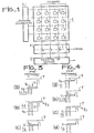
- FIG. 1 is the diagram of a photosensitive device with line tramsfer according to the prior art.
- a photosensitive zone 1 is represented schematically, consisting of a matrix of M lines each comprising N photosensitive points P.
- This zone receives the light image to be analyzed and transforms it into electrical charges, called signal charges Q s .
- the photosensitive points of the same line are connected to each other as well as to an address register 2 which makes it possible to select a line of the matrix which will be read.
- the photosensitive points of a column are connected by the same conductive column.
- the conductive columns lead to a memory 4.
- This memory includes switching means symbolized by switches 1 and leading the charges located on the conductive columns either to an evacuation drain or to a read register 3.
- the memory provides periodically the transfer to the reading register of the signal charges collected on a line of photosensitive dots and transferred to the columns. In addition, the memory periodically ensures the transfer to a drain of parasitic charges on the columns before the arrival on the columns of the signal charges of one of the lines.
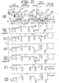
- FIGS. 2a to g are diagrams illustrating the operation of a device according to the prior art. These figures have been described in great detail in French patent application No. 2,481,553 to which reference will be made if necessary. We will only recall that the figure 2a is a view in longitudinal section of the photosensitive device represented in FIG. 1 of the cited patent application and that FIGS. 2b to g represent the evolution of the surface potential 0 s in the semiconductor substrate 4 at various times t, at t s .
- each photosensitive point is constituted by the association of a photo-MOS, constituted by a photosensitive grid G o , and of a photodiode D 10 .
- FIGS. 3a to c and 4a to d are diagrams illustrating two variants of the method according to the invention in the case of photosensitive dots formed as in FIG. 2a by the association of a photo-MOS and a photodiode. Like Figures 2b to g, these figures show the evolution of the surface potential in the substrate at various times, but we were only interested in what happens at the photosensitive points because the functioning of the rest of the device is not changed.
- the storage capacity of the photosensitive points is temporarily modified so that they can store charges in the time interval T, even if they are dazzled.
- the photosensitive dots even if they are illuminated, do not overflow onto the columns.
- the storage capacity of the photosensitive dots is increased during the time interval T.
- This increase in storage capacity can be obtained by acting on the bias voltage of the photosensitive points.
- the semiconductor substrate 4 is of the P type, it suffices to increase the bias voltage Vg applied to the gates G o to increase the storage capacity of the photosensitive points.
- the depth of the potential wells for the photosensitive points is then at level V M whereas it is at level V, less than V M , at time t l .
- the photosensitive points of this line receive by the addressing register the reference potential of the device as shown in FIG. 3b where the situation of the other photosensitive points is shown in dotted lines.
- the photosensitive points even if they are illuminated, do not overflow onto the columns.
- the storage capacity of the photosensitive dots is reduced during the evacuation of the parasitic charges from the conductive columns to the memory, then we return to the normal storage capacity of the photosensitive dots the beginning of the interval T.
- the storage capacity of the photosensitive points is reduced.
- the level of the potential wells goes from level V to level V n which is lower there. This can be achieved by decreasing the bias voltage grids G o . It suffices to decrease the storage capacity of the photosensitive points for a short time.
- the points which were already saturated, or about to be saturated are rid of a part of their charges which is evacuated towards the drain. All the photosensitive points are therefore ready to store new charges.
- the photosensitive points are given their normal storage capacity.
- the level of the potential wells goes from V m to V.
- the photosensitive points even if they are dazzled, are therefore able to store an amount of charge equal to that which has been evacuated by contraction capacity at time t 1 and there is no overflow of parasitic charges on the columns.
- This method applies in the manner just described when the photosensitive points are only constituted by photo-MOS, and do not include photodiodes.
- the storage capacity of the photosensitive points is modified by acting on the bias voltage of the grids of the photo-MOS.
- each photosensitive point therefore comprises a photodiode D 10 , integrated on the semiconductor substrate 4 of type P and separated from a diode D 1 connected to a column Ci by a grid G 1 which is not subjected to radiation and which receives a bias voltage.
- the bias voltage of the gate G 1 has a value V2 equal for example to + 1V.
- V2 the bias voltage of the gate G 1
- the grid G 1 then isolates each photodiode from the diodes D 1 connected to the columns, as shown in dotted lines in FIG. 2b where the increasing surface potentials are directed downwards.
- the bias voltage of the gate G 1 takes a value V 1 , equal for example to 10 V and there is transfer of the charges-signal on the diodes D1.
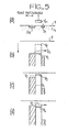
- FIG. 5c illustrates the variant of the method according to the invention corresponding to that which is shown in FIG. 3.
- the bias voltage of the gate G 1 takes a value V 3 equal for example to 0.5 V and therefore less than V 2 , which increases the storage capacity of the photosensitive points.
- V 3 the bias voltage of the gate G 1 takes a value V 3 equal for example to 0.5 V and therefore less than V 2 , which increases the storage capacity of the photosensitive points.
- this situation continues during the interval T, except for the photosensitive points whose content is transferred into memory and for which the bias voltage of the grid takes the value V 1 .
- FIG. 5d illustrates the variant of the method according to the invention corresponding to that which is shown in FIG. 4, this variant is easier to implement than that of FIG. 5c.
- the gate G 1 Before the start of the interval T, at time t 1 , the gate G 1 receives a bias voltage V 4 , equal for example to 2 V and therefore greater than V 2 . This reduces the storage capacity of photosensitive spots. From the start of the interval T, the photosensitive points are given their normal storage capacity by giving the bias voltage the value V 2 .
Landscapes
- Engineering & Computer Science (AREA)
- Multimedia (AREA)
- Signal Processing (AREA)
- Solid State Image Pick-Up Elements (AREA)
- Transforming Light Signals Into Electric Signals (AREA)
Applications Claiming Priority (2)
| Application Number | Priority Date | Filing Date | Title |
|---|---|---|---|
| FR8221866A FR2538650A1 (fr) | 1982-12-28 | 1982-12-28 | Procede d'analyse d'un dispositif photosensible a transfert de ligne |
| FR8221866 | 1982-12-28 |
Publications (2)
| Publication Number | Publication Date |
|---|---|
| EP0113627A1 EP0113627A1 (fr) | 1984-07-18 |
| EP0113627B1 true EP0113627B1 (fr) | 1986-09-24 |
Family
ID=9280557
Family Applications (1)
| Application Number | Title | Priority Date | Filing Date |
|---|---|---|---|
| EP83402487A Expired EP0113627B1 (fr) | 1982-12-28 | 1983-12-20 | Procédé d'analyse d'un dispositif photosensible à transfert de ligne |
Country Status (5)
| Country | Link |
|---|---|
| US (1) | US4645938A (enExample) |
| EP (1) | EP0113627B1 (enExample) |
| JP (1) | JPS59134873A (enExample) |
| DE (1) | DE3366489D1 (enExample) |
| FR (1) | FR2538650A1 (enExample) |
Families Citing this family (4)
| Publication number | Priority date | Publication date | Assignee | Title |
|---|---|---|---|---|
| FR2608315B1 (fr) * | 1986-12-16 | 1989-02-17 | Thomson Csf | Dispositif anti-eblouissement pour capteur d'images a transfert de charges et capteur d'images comportant un tel dispositif |
| US4956716A (en) * | 1989-02-21 | 1990-09-11 | Santa Barbara Research Center | Imaging system employing charge amplifier |
| FR2653626A1 (fr) * | 1989-10-24 | 1991-04-26 | Thomson Composants Militaires | Capteur photosensible a temps d'integration programmable. |
| KR970705894A (ko) * | 1995-06-23 | 1997-10-09 | 요트.게.아.롤페즈 | CCD 이미저를 동작시키는 방법과 이러한 방법을 수행시키기에 적합한 CCD 이미저(Method Of operating a CCD imager, and CCD imager suitable for the imple-mentation of such a method) |
Family Cites Families (5)
| Publication number | Priority date | Publication date | Assignee | Title |
|---|---|---|---|---|
| JPS583630B2 (ja) * | 1977-09-16 | 1983-01-22 | 松下電子工業株式会社 | 固体光像検出装置 |
| JPS6033345B2 (ja) * | 1979-06-08 | 1985-08-02 | 日本電気株式会社 | 電荷転送撮像装置とその駆動方法 |
| JPS56164681A (en) * | 1980-05-22 | 1981-12-17 | Matsushita Electronics Corp | Solidstate image pick-up device |
| FR2504334B1 (fr) * | 1981-04-16 | 1985-10-18 | Thomson Csf | Dispositif d'analyse d'image en lignes successives, utilisant le transfert de charges electriques, composant une memoire de ligne, et camera de television comportant un tel dispositif |
| DE3138294A1 (de) * | 1981-09-25 | 1983-04-14 | Siemens AG, 1000 Berlin und 8000 München | Zweidimensionaler halbleiter-bildsensor mit steuerung oder regelung der integrationszeit |
-
1982
- 1982-12-28 FR FR8221866A patent/FR2538650A1/fr active Granted
-
1983
- 1983-12-16 US US06/562,443 patent/US4645938A/en not_active Expired - Lifetime
- 1983-12-20 DE DE8383402487T patent/DE3366489D1/de not_active Expired
- 1983-12-20 EP EP83402487A patent/EP0113627B1/fr not_active Expired
- 1983-12-26 JP JP58252238A patent/JPS59134873A/ja active Pending
Also Published As
| Publication number | Publication date |
|---|---|
| US4645938A (en) | 1987-02-24 |
| JPS59134873A (ja) | 1984-08-02 |
| FR2538650A1 (fr) | 1984-06-29 |
| FR2538650B1 (enExample) | 1985-03-08 |
| DE3366489D1 (en) | 1986-10-30 |
| EP0113627A1 (fr) | 1984-07-18 |
Similar Documents
| Publication | Publication Date | Title |
|---|---|---|
| EP3188238B1 (fr) | Pixel de détection de temps de vol | |
| US4430672A (en) | Photosensitive device read by charge transfer | |
| EP2962330B1 (fr) | Capteur d'image avec grille d'anti-eblouissement | |
| EP0064890B1 (fr) | Dispositif d'analyse d'image en lignes successives, utilisant le transfert de charges électriques, comportant une mémoire de ligne, et caméra de télévision comportant un tel dispositif | |
| EP0113627B1 (fr) | Procédé d'analyse d'un dispositif photosensible à transfert de ligne | |
| FR2963187A1 (fr) | Dispositif d'imagerie a performances ameliorees et procede de commande. | |
| EP0341122A1 (fr) | Photodétecteur matriciel à transfert de charges avec dispositif intégré de filtrage de charges | |
| EP0474550A1 (fr) | Détecteur d'images à pixels de grandes dimensions | |
| EP0114768B1 (fr) | Dispositif photosensible à transfert de charge | |
| JP2771221B2 (ja) | 感光ドットマトリクス | |
| EP0410465B1 (en) | Solid state image pickup device having photo-shield plate in contact with photo-electric converting region via Schottky barrier | |
| FR2598019A1 (fr) | Procede d'utilisation d'une matrice photosensible a transfert de charge, et matrice photosensible ainsi utilisee | |
| EP0251386A1 (fr) | Dispositif à transfert de charges (DTC) à éliminateur du niveau de fond d'un signal détecté, structure de détection et procédé d'utilisation d'un tel DTC | |
| EP0276594A1 (fr) | Dispositif anti-éblouissement pour capteur d'images à transfert de charges, et capteur d'images comportant un tel dispositif | |
| FR2513015A1 (fr) | Dispositif de detection d'image en couleurs du type transfert de charge | |
| EP0068947B1 (fr) | Ensemble détecteur photonique, lecteur à transfert de charges adapté, et cible de prise de vues utilisant un tel ensemble | |
| EP0323924B1 (fr) | Procédé et circuit de lecture à faible bruit pour matrice photosensible à transfert de ligne | |
| EP0141695B1 (fr) | Dipositif photosensible à transfert de ligne | |
| EP0182679A1 (fr) | Dispositif photosensible à transfert de ligne muni d'amplificateurs de contre-réaction | |
| FR2668303A1 (fr) | Capteur optique a faible diaphotie. | |
| EP0329518B1 (fr) | Dispositif de lecture de charges pour capteur photosensible linéaire, avec dispositif d'antiéblouissement à structure en ligne | |
| FR2488085A1 (fr) | Dispositif de commutation pour la decharge d'une capacite, et camera de prise de vues comprenant ce dispositif | |
| EP0390644A1 (fr) | Registres de lecture du type à transfert de charges à grande dynamique de sortie | |
| JPH07105919B2 (ja) | 固体撮像装置の駆動方法 | |
| US5477069A (en) | Charge transfer device and driving method for the same |
Legal Events
| Date | Code | Title | Description |
|---|---|---|---|
| PUAI | Public reference made under article 153(3) epc to a published international application that has entered the european phase |
Free format text: ORIGINAL CODE: 0009012 |
|
| AK | Designated contracting states |
Designated state(s): DE GB NL |
|
| 17P | Request for examination filed |
Effective date: 19840804 |
|
| GRAA | (expected) grant |
Free format text: ORIGINAL CODE: 0009210 |
|
| AK | Designated contracting states |
Kind code of ref document: B1 Designated state(s): DE GB NL |
|
| REF | Corresponds to: |
Ref document number: 3366489 Country of ref document: DE Date of ref document: 19861030 |
|
| R20 | Corrections of a patent specification |
Effective date: 19861022 |
|
| PLBE | No opposition filed within time limit |
Free format text: ORIGINAL CODE: 0009261 |
|
| STAA | Information on the status of an ep patent application or granted ep patent |
Free format text: STATUS: NO OPPOSITION FILED WITHIN TIME LIMIT |
|
| 26N | No opposition filed | ||
| REG | Reference to a national code |
Ref country code: GB Ref legal event code: IF02 |
|
| PGFP | Annual fee paid to national office [announced via postgrant information from national office to epo] |
Ref country code: GB Payment date: 20021218 Year of fee payment: 20 |
|
| PGFP | Annual fee paid to national office [announced via postgrant information from national office to epo] |
Ref country code: NL Payment date: 20021227 Year of fee payment: 20 |
|
| PGFP | Annual fee paid to national office [announced via postgrant information from national office to epo] |
Ref country code: DE Payment date: 20021231 Year of fee payment: 20 |
|
| PG25 | Lapsed in a contracting state [announced via postgrant information from national office to epo] |
Ref country code: GB Free format text: LAPSE BECAUSE OF EXPIRATION OF PROTECTION Effective date: 20031219 |
|
| PG25 | Lapsed in a contracting state [announced via postgrant information from national office to epo] |
Ref country code: NL Free format text: LAPSE BECAUSE OF EXPIRATION OF PROTECTION Effective date: 20031220 |
|
| REG | Reference to a national code |
Ref country code: GB Ref legal event code: PE20 |
|
| NLV7 | Nl: ceased due to reaching the maximum lifetime of a patent |
Effective date: 20031220 |