EP0112218B1 - Dispositif électronique de mesure avec filtrage passe-bas accéléré, en particulier pour le pesage - Google Patents
Dispositif électronique de mesure avec filtrage passe-bas accéléré, en particulier pour le pesage Download PDFInfo
- Publication number
- EP0112218B1 EP0112218B1 EP83402278A EP83402278A EP0112218B1 EP 0112218 B1 EP0112218 B1 EP 0112218B1 EP 83402278 A EP83402278 A EP 83402278A EP 83402278 A EP83402278 A EP 83402278A EP 0112218 B1 EP0112218 B1 EP 0112218B1
- Authority
- EP
- European Patent Office
- Prior art keywords
- signal
- output
- fact
- stage
- input terminal
- Prior art date
- Legal status (The legal status is an assumption and is not a legal conclusion. Google has not performed a legal analysis and makes no representation as to the accuracy of the status listed.)
- Expired
Links
- 238000005303 weighing Methods 0.000 title claims description 25
- 238000001914 filtration Methods 0.000 title claims description 15
- 230000010355 oscillation Effects 0.000 claims description 27
- 239000003990 capacitor Substances 0.000 claims description 26
- 230000007935 neutral effect Effects 0.000 claims description 12
- 230000015654 memory Effects 0.000 claims description 7
- 230000005669 field effect Effects 0.000 claims description 6
- 230000002045 lasting effect Effects 0.000 claims description 4
- 230000004069 differentiation Effects 0.000 claims 3
- 238000010586 diagram Methods 0.000 description 13
- 238000005259 measurement Methods 0.000 description 10
- 241001465754 Metazoa Species 0.000 description 2
- XUIMIQQOPSSXEZ-UHFFFAOYSA-N Silicon Chemical compound [Si] XUIMIQQOPSSXEZ-UHFFFAOYSA-N 0.000 description 2
- 238000006243 chemical reaction Methods 0.000 description 2
- 230000001419 dependent effect Effects 0.000 description 2
- 230000003071 parasitic effect Effects 0.000 description 2
- 230000010363 phase shift Effects 0.000 description 2
- 230000000135 prohibitive effect Effects 0.000 description 2
- 239000004065 semiconductor Substances 0.000 description 2
- 229910052710 silicon Inorganic materials 0.000 description 2
- 239000010703 silicon Substances 0.000 description 2
- 238000012360 testing method Methods 0.000 description 2
- 230000007704 transition Effects 0.000 description 2
- 241000897276 Termes Species 0.000 description 1
- 230000002301 combined effect Effects 0.000 description 1
- 238000012937 correction Methods 0.000 description 1
- 230000003247 decreasing effect Effects 0.000 description 1
- 238000011161 development Methods 0.000 description 1
- 230000000694 effects Effects 0.000 description 1
- 235000021183 entrée Nutrition 0.000 description 1
- 235000013305 food Nutrition 0.000 description 1
- 235000012054 meals Nutrition 0.000 description 1
- 229910044991 metal oxide Inorganic materials 0.000 description 1
- 150000004706 metal oxides Chemical class 0.000 description 1
- 238000000034 method Methods 0.000 description 1
- 238000012544 monitoring process Methods 0.000 description 1
- 210000000056 organ Anatomy 0.000 description 1
- 235000012830 plain croissants Nutrition 0.000 description 1
- 230000000750 progressive effect Effects 0.000 description 1
- 230000004044 response Effects 0.000 description 1
- 230000000630 rising effect Effects 0.000 description 1
Images
Classifications
-
- G—PHYSICS
- G01—MEASURING; TESTING
- G01G—WEIGHING
- G01G23/00—Auxiliary devices for weighing apparatus
- G01G23/06—Means for damping oscillations, e.g. of weigh beams
- G01G23/10—Means for damping oscillations, e.g. of weigh beams by electric or magnetic means
Definitions
- the present invention relates to low-pass filtering of analog signals, and applies in particular to weighing with digital display.
- the present invention makes it possible to solve this problem, by proposing a new electronic measurement device with low-pass filtering, applicable in particular to weighing.
- this device has, between active input and output terminals and ground, a network of resistive and reactive elements arranged in low-pass filtering quadrupole.
- the controlled resistance mesh comprises a field effect transistor
- the control means comprise a circuit with double time constant capable of causing the transistor to drive quickly after the end of the neutral time interval , and then bring it back to the blocked state in a progressive manner.
- control means comprise a circuit connected to the input terminal, in order to apply to the transistor gate a conduction control voltage close to the voltage present on the input terminal.
- the controlled resistance mesh and the double time constant circuit are arranged so that the variation slope of the time constant of the filtering quadrupole remains less than the minimum frequency to be filtered.
- the minimum frequency to be filtered is of the order of Hertz.
- a vibration of 1 Hz is eliminated, which supposes an even lower minimum (cut-off) frequency.
- the discriminator means comprise a high gain oscillation amplifier stage, at least with weak signals, connected to the input terminal, a comparator stage connected firstly to the input terminal, and on the other hand at the output of the oscillation amplifier, and a differentiating stage connected to the output of the comparator stage, said niche signal being defined from the lasting absence of pulses at the output of the 'differentiating stage.
- the delay means advantageously comprise a resettable monostable circuit, connected to the output of the differentiating stage, this resettable monostable circuit providing as output the signal in square wave decreased at its beginning of the neutral time interval, of duration predetermined.
- the device is mounted between a weight sensor circuit and an analog-digital weighing converter.
- the analog-digital weighing converter is followed by control logic associated with memories, a keyboard and a digital display; the logic reacts to a specific command from the keyboard by receiving address information from it from memory, then putting the newly determined weight at this address while displaying the difference between the previously stored weight and the newly determined weight .
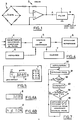
- Fig. 1 illustrates a conventional weighing arrangement for digital display.
- the load receptor (not shown) has for example the ring structure described in patent application FR 2469701, fitted with strain gauges as sensors. These strain gauges are arranged in a bridge 3, followed by an amplifier stage 2, then by a filter 1, the output of which is applied to an analog-digital converter of weight 4 (fig. 4).
- the filters 1 used up to now include, for example, two low-pass R-C cells in series.
- the present invention proposes an improved electronic filter, which generally allows accelerated obtaining of a measurement signal free of oscillations.
- this filter solves the specific problem linked to the presence of untimely or inevitable oscillations, affecting the support of the weighing instrument and / or the body to be weighed.
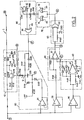
- This filter illustrated in fig. 2, will replace the block 1 of FIG. 1, at least for weighing applications.
- the filter comprises an active input terminal A, an active output terminal B, and of course a ground, which also appear in FIG. 1.
- a quadrupole generally designated by 10, and consisting of two RC elements in series, the first comprising the resistor R12 followed by the capacitor C12 in parallel on the ground, and the second comprising the resistor R13 followed by capacitor C14 also in parallel on ground.
- This controlled resistance mesh consists here of a resistor R15, in series on the source-drain mesh of a field effect transistor Q16.
- the transistor Q16 is of the metal-oxide semiconductor type with insulated gate and with P channel.
- the resistance values are for example 2.2 megohms for R12, 100 kilohms for R13, and 5 kilohms for R15.
- the capacity values are 2.2 microfarads for C12, and 0.33 microfarads for C14.
- the field effect transistor is for example the J271 model from the company “Siliconix” or “National Semi-Conductor”.
- the set R12 and C12 corresponds to a time constant of 4.84 s.
- the set R13 and C14 corresponds to a time constant of 33 ms, thus ensuring additional filtering, in particular because of the switches printed on the first part of the filter.
- the present invention further provides for a particular control of the variation of the time constant linked to the mesh R15 Q16.
- the signal present on the active input terminal A is applied to three stages forming a buffer amplifier, noted respectively 21, 35 and 36.
- the stages 35 and 36 are part of discriminating means, which also incorporate blocks 40, 50 and 60 of fig. 2. These discriminating means are sensitive to the signal present on terminal A, in order to provide a signal of the slot type following a variation of the DC component of the signal present on the active input terminal A. According to an interesting aspect of the invention , the duration of this niche signal increases with the amplitude of the variation in question of the DC component.
- the discriminator means here comprise a high gain oscillation amplifier stage, at least in weak signals, referenced 40.
- This stage 40 is connected to the input terminal A by the buffer stage 36. It is followed a comparator 50, also connected to the input terminal A through the other buffer stage 35. Finally, a differentiator stage 60 is connected to the output of the comparator stage 50. At the output of the differentiator 60, the The above-mentioned niche signal is defined on the basis of the lasting absence of pulses.
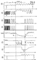
- Line A of fig. 3 represents an input signal assumed to be applied to terminal A.
- this signal consists of a first part I, consisting of a strictly constant voltage of value V, and free of oscillations. Then, in part II, a low frequency oscillation is superimposed on the continuous signal V l .
- Part III the continuous component in mean value of the signal increases, to pass to a value V 2 , while continuing to be animated by over-oscillations.
- block 40 consists of a differential chopper amplifier with very high input impedance, noted 41.
- This amplifier is for example the ICL 7650CPD model, sold by the company "Intersil".
- This amplifier normally has an open loop gain of the order of 10 6 , and an input impedance of the order of 10 10 ohms. In known manner, it is provided with two auxiliary capacities denoted C45 in FIG. 2.
- the non-inverting input of the amplifier 41 is connected to the terminal A via the buffer stage 36, through a series resistor R43, for example equal to 2.2 megohms, and followed by a parallel capacitance C44 , worth for example 330 nanofarads. It will be observed that this corresponds to a time constant of approximately 0.73 s.
- the inverting input of the amplifier 41 is connected to the output of the stage 36 by a resistor R42 measuring for example 4.7 kilohms.
- This same inverting input is connected to the output of the amplifier 41 by a non-linear diode feedback, comprising two diodes D46 in series in one direction, and two diodes D47 in series in the other direction.
- These diodes are preferably silicon diodes such as the model 1 N4148.
- the stage 40 thus mounted has the property of having a practically unity gain for the continuous input signals. Indeed, the impedance of the non-inverting input as well as of the inverting input is very large even compared to the internal resistance of the diodes D46 and D47. In addition, the current which will pass through the resistors R42 and R43 as well as the diodes D46 and D47 will also be very low taking into account the input impedance of the amplifier 41. In direct current, the two inputs of the amplifier being at the same potential the output follows the inputs.
- this threshold frequency is of the order of 0.2 Hertz, subject to the effects due to the large gain of the amplifier, to its linear counteraction, and to the other resistances involved.
- the high gain oscillation amplifier stage 40 is followed by a comparator stage 50, the output of the amplifier 41 being connected to the inverting input of comparator 51.
- the non-inverting input of this same comparator is connected d on the one hand at the output of the buffer stage 35 by a resistor R52, and on the other hand at the output of the comparator 51 by a resistor R53.
- the resistance R53 is significantly larger than the resistance R52, typically by a factor of around 500, which gives this comparator 51 operation at low hysteresis.
- the comparator stage 50 will therefore compare the input signal A with the signal at point C, shown in the first two diagrams of FIG. 3.
- phase I the peak-to-peak amplitude at the output at point C is high, which will produce a very rapid alternating passage of the output of the comparator stage 50 between these two extreme voltages. This is done at the frequency of the noise, therefore at a very high frequency.
- phase II things happen in the same way, but at the frequency of the oscillations superimposed on the DC component of the signal A. We therefore obtain a rectangular signal.
- the signal at point C remains permanently higher than the input signal A.
- the signal at point C is applied to the inverting input of comparator 51, which remains permanently with an output at low level.
- the signal at point A After a certain time, linked to the speed of reappearance of the oscillations at point C, the signal at point A again becomes higher at times than the signal at point C. This begins, in the example shown where the continuous component has increased, by an overshoot which takes place on the negative half-waves of signal A. We therefore see appear at point D, as shown in the third diagram in FIG. 3, pulses which appear at each negative alternation of the signal A, and have a progressively increasing duration until reaching the entire duration of the negative alternation. The steady state which is then reached is the same as that which existed at point D during phase II.
- the signal D is then applied to a differentiator stage 60, connected to the output of the comparator stage 50.
- the differentiating stage 60 is formed from an EXCLUSIVE OR gate 61, one input of which directly receives the output of stage 50, while the other receives the same output through a network RC consisting of the R62 series resistor and the C63 capacitor in parallel to ground.
- This RC network will produce a phase shift between the two inputs of gate 61. Consequently, any rapid transition appearing in signal D will result in the appearance of a pulse on signal E available at the output of gate 61.
- This signal E is illustrated in diagram E of FIG. 3. It comprises multiple pulses close together opposite the part of signal A. With regard to part II, it comprises pulses substantially at the level of each zero crossing of signal A. At the start of part III, no pulse n 'appears.
- the pulses reappear when the signal D also reappears. These pulses are at the start two close pulses, separated by a slightly larger time interval from the following two close pulses. And as we recover the steady state with a peak-to-peak amplitude V3 in signal C, the pulses of signal E again become regularly distributed over time.
- the previously mentioned slot signal is defined from the lasting absence of pulses in signal E, that is to say at the output of the differentiating stage. It has been observed previously that the return of signal C to its normal peak-to-peak amplitude V3 is all the longer as the variation of the DC component of signal A is greater. Correlatively, the duration of the slot signal present in the signal E is also all the longer as the variation of the DC component is greater.
- the signal E is applied to an intermediate amplifier stage 70, constituted here by two EXCLUSIVE gates 71 and 72 connected in parallel. One of the inputs of each door receives the signal E, the other receives the ground. Those skilled in the art will understand that the output of stage 70 reproduces the shape of signal E, but with greater energy.
- this resettable monostable circuit is based on a capacitor C85, mounted in parallel on a resistor R83, one of the terminals of this set being connected to ground.
- the opposite terminal of the same assembly is connected by a resistor R84 to the cathode of a diode D82 whose anode receives the output of stage 70.
- the hot spot common to the capacitor C85 and to the resistors R83 and R84 is connected to an input of an EXCLUSIVE OR door 81, the other input of which is connected to ground.
- the capacitance of the capacitor C85 is for example equal to 1 microfarad, while the values of the resistors R83 and R84 are very different, the resistance R84 being worth for example 4.7 kilohms, while the resistance R84 is worth 1 megohm. It follows that the output of stage 70 will charge the capacitor C85 with a fast time constant, essentially dependent on the resistance R84, while this same capacitor will discharge with a slow time constant, essentially dependent on the resistance R83.
- the resettable monostable circuit 80 defines a neutral time interval, of predetermined duration T l , consecutively at the start of the slot signal.
- the signal at point F will return to its maximum value.
- the first pulse which reappears in the signal E is most of the time insufficient to sufficiently recharge the capacitor C85 so as to detectably exceed the voltage V o , and to toggle the gate 81.
- this will happen at the level of the second pulse, or possibly at the level of a following pulse.
- Diagram F of fig. 3 admits that this tilting occurs at the level of the second pulse, therefore with a delay T 2 with respect to the first pulse and at the end of the signal-slot. This delay is mainly related to the value of the time constant defined by the product R84xC85.
- the duration of the neutral time interval is chosen at least equal to the value of the half-period corresponding to the lowest frequency which it is desired to filter. For example, if the limit frequency to be filtered is 1 Hz, the duration of the neutral time interval is at least equal to 0.5 s.
- the time interval T 2 is not critical, it can however advantageously be as short as possible.
- One way of doing this is to use an integrated circuit forming a resettable monostable, rather than the detailed embodiment of stage 80 as it appears in FIG. 2.
- the signal F consists of the output of a logic gate, and therefore varies between a higher value of approximately 8 V and a lower value close to 0 V.
- the signal F available at the output of the monostable stage 80 is applied on the one hand to the cathode of a diode D29, the anode of which is connected to a resistor R28, which in turn is connected to the point Q.
- the point F is also connected directly to point Q through a resistor R27 with a value significantly higher than that of R28.
- the resistor R27 is worth 270 kilohms
- the resistor R28 is worth 12 kilohms.
- the point Q is connected by a resistor R26 measuring for example 47 kilohms the gate of the field effect transistor Q16.
- the same point Q is connected on the one hand to the positive armature of an electrochemical capacitor C23 whose negative armature is connected by a resistor R25 to the voltage of +8 V constituting the supply.
- the point Q is connected on the other hand to the cathode of a diode D24 whose anode is also connected to the point P forming the common point between the negative pole of the capacitor C23 and the resistor R25.
- this same point P is connected to the anode of a diode D22 whose cathode goes to the output of the buffer amplifier stage 21 already mentioned, which has a gain 1 and whose non-inverting input is as for the other buffer amplifiers connected to point A.
- the signal F is in steady state at the value of +8 V.
- This voltage is transferred to point Q through the resistor R27. It therefore appears on the positive armature of capacitor C23.
- the point P, or negative armature of the capacitor C23 follows the voltage present at point A, increased by the value of the threshold voltage of the diode D22, that is to say about 0.6 V, in the case of a silicon diode.
- the capacitor C23 is therefore charged substantially according to the difference between the voltage present at point F and the voltage present at point A (except the 0.6 V of the diode D22, and the fact that the signal at point F is slightly less than 8 V).
- This voltage at point Q is therefore applied to the isolated gate of transistor Q16, which is blocked and therefore has a very high impedance between the resistor R15 and the common point of the resistor R12 and of the capacitor C12.
- the filtering properties of the quadrupole 10 are then only defined by the resistor R12 and the capacitor C12 for its first section, and by the resistor R13 and the capacitor C14 for its second section. Given the numerical values previously given, it is the network R12 C12 which predominates, and defines a time constant of the order of 5 s (the product is worth exactly 4.84 s).
- Diagram G of fig. 3 illustrates that during the time interval T i , for which the signal F remains at approximately +8 V, at the start of phase III, the transistor Q16 remains blocked. Under these conditions, the signal B which represents the output of the filtering quadrupole will increase very slightly, starting to follow the variation of the DC component of the signal A, but with a very large "inertia".
- the signal F changes state, suddenly passing to a value close to zero.
- the capacitor C23 of stage 20 then suddenly discharges through resistor R28 and diode D29.
- the transistor Q16 becomes conductive, and it is then the resistor R15 which defines with the capacitor C12 the time constant of the quadrupole 1 in its first section. As previously indicated, this time constant is 11 ms. Oscillations appear immediately output on signal B. These oscillations quickly acquire an amplitude and an average value in accordance with those of signal A. This state of affairs lasts until signal F rises to +8 V.
- Tests were carried out with a weighing instrument having 2000 measurement points for a maximum range of 10 kg, that is to say a resolution of 5 g on the digital display.
- the balance pan was subjected to a vibration at the frequency of 1 Hz, with an amplitude of ⁇ 100 steps, ie ⁇ 500 g.
- a weight of known value was then placed on the pan. The exact value of this weight was obtained in 7 s.
- the measuring chain according to the present invention is obtained in the following manner: the filter 1 of FIG. 1 is replaced. 1 by the filter according to the invention illustrated in FIG. 2, and the output of this filter is applied to the analog-digital converter of weight 4 of FIG. 4.
- the high precision obtained, within a reasonable time, makes it possible to envisage low differential measurements.
- the converter 4 is connected to a control logic, interconnected on its side with memories 6 and a keyboard 7, and driving the digital display 8.
- the keyboard 7 and the digital display 8 are illustrated in FIG. 5, which represents for example the front face of a baby scale.
- the keyboard 7 comprises the conventional numerical digits, plus a command C allowing correction, and a return to the display of the weight, and a key E allowing the recording of the weight.
- the digital display 8 has 4 digits on the right, which are significant for displaying the weight from 0 to 10 kg per 5g increments.
- a decimal point indicates that the weighing zero is correct.
- there is an additional display area which makes it possible to display address information such as a bed number, this information being entered at the level of the keyboard 7 in the manner described below.
- the normal regime consists in displaying the weight in step 91.
- the display then presents the form of FIG. 6A, assuming a weight of 3285 g.
- test 92 examines whether the operator has pressed the key E. If not, the weight is continued to be displayed. If yes, we go to the display of E at the address location on display 8.
- the logic is then awaiting the introduction of the bed number, or the address, by the operator using the keyboard 7. It is assumed here that the operator enters the bed number or address 4. If no bed number is entered, the logic can remain on hold, or preferably return to the display of the weight in 91, after a predetermined time equal for example to one minute.
- step 95 consists in displaying the bed number in the display (fig. 6B).
- the display is completed by the letter "d", indicating that the rest of the display is going to be a weight difference.
- the control unit 5 then makes the difference between the new weight and the old weight available in memory 6 at address 4. It is assumed here that this difference is equal to 104 g, and it is therefore displayed as shown in a fig. 6B.
- the control logic replaces in memory 6, and at address 4, the new weight value, that is 3285 g. We then return to the normal regime which is the display of the weight in 91.
- the present invention applies particularly well to the case of baby scales, but it is not limited to this application, and can also be used for weighing animals, as well as for any other weighing where the plate is animated by parasitic oscillations. Conversely, the invention can also be used when it is not the pan but the support of the balance which is animated by oscillations, as is the case for example during weighing in a delivery truck.
- circuits 10, 20, 40, 50, 60, 70 and 80 can be replaced by any equivalent means.
Landscapes
- Physics & Mathematics (AREA)
- General Physics & Mathematics (AREA)
- Networks Using Active Elements (AREA)
Applications Claiming Priority (2)
| Application Number | Priority Date | Filing Date | Title |
|---|---|---|---|
| FR8220201 | 1982-12-02 | ||
| FR8220201A FR2537276A1 (fr) | 1982-12-02 | 1982-12-02 | Dispositif electronique de mesure avec filtrage passe-bas accelere, en particulier pour le pesage |
Publications (2)
| Publication Number | Publication Date |
|---|---|
| EP0112218A1 EP0112218A1 (fr) | 1984-06-27 |
| EP0112218B1 true EP0112218B1 (fr) | 1986-11-20 |
Family
ID=9279717
Family Applications (1)
| Application Number | Title | Priority Date | Filing Date |
|---|---|---|---|
| EP83402278A Expired EP0112218B1 (fr) | 1982-12-02 | 1983-11-25 | Dispositif électronique de mesure avec filtrage passe-bas accéléré, en particulier pour le pesage |
Country Status (5)
| Country | Link |
|---|---|
| US (1) | US4531600A (enExample) |
| EP (1) | EP0112218B1 (enExample) |
| CA (1) | CA1191613A (enExample) |
| DE (1) | DE3367810D1 (enExample) |
| FR (1) | FR2537276A1 (enExample) |
Families Citing this family (12)
| Publication number | Priority date | Publication date | Assignee | Title |
|---|---|---|---|---|
| EP0122796B1 (en) * | 1983-04-14 | 1989-08-02 | Kabushiki Kaisha Ishida Koki Seisakusho | Weighing apparatus |
| JPS60228926A (ja) * | 1984-04-26 | 1985-11-14 | Tokyo Electric Co Ltd | ラベルプリンタ付き電子料金秤 |
| GB2173308B (en) * | 1985-04-02 | 1988-12-29 | Shinko Denshi Kk | Weight measuring apparatus of vibration type |
| US4705126A (en) * | 1985-09-24 | 1987-11-10 | Ishida Scales Manufacturing Company, Ltd. | Signal processing circuit and weighing apparatus incorporating same |
| US4696359A (en) * | 1986-08-22 | 1987-09-29 | National Transducer Corporation | Electronic weighing apparatus |
| US4967384A (en) * | 1988-03-14 | 1990-10-30 | General Electrodynamics Corporation | Highly accurate weighing system |
| US4909340A (en) * | 1989-02-03 | 1990-03-20 | John Chatillon & Sons Inc. | Electronic weighing scale |
| US4991446A (en) * | 1989-10-05 | 1991-02-12 | Metriguard, Inc. | Force measurement with compensation of errors caused by accelerations of measuring apparatus |
| US5131482A (en) * | 1989-12-28 | 1992-07-21 | General Electrodynamics | Self-contained weighing system and method |
| EP2071304A4 (en) * | 2006-09-27 | 2010-11-17 | Shimadzu Corp | ELECTRONIC SCALE |
| CN100489466C (zh) * | 2007-08-10 | 2009-05-20 | 中国航天科技集团公司第四研究院第四十四研究所 | 车辆动态轴重衡称重信号的自适应滤波方法 |
| CN103424167B (zh) * | 2012-05-21 | 2016-08-03 | 梅特勒-托利多(常州)测量技术有限公司 | 利用整车计量车辆衡计算轴重的方法 |
Family Cites Families (9)
| Publication number | Priority date | Publication date | Assignee | Title |
|---|---|---|---|---|
| US3525991A (en) * | 1966-06-15 | 1970-08-25 | Toledo Scale Corp | Converter |
| US3434343A (en) * | 1967-04-03 | 1969-03-25 | Blh Electronics | Low frequency damping circuit for strain gage transducers |
| GB1407195A (en) * | 1971-10-21 | 1975-09-24 | Barton M | Electronic weighing apparatus |
| DE2205778A1 (de) * | 1972-02-08 | 1973-08-16 | Boekels & Co H | Schaltungsanordnung zum einsatz an elektrischen messwertgebern, insbesondere elektro-mechanischen waagen |
| GB1356069A (en) * | 1972-04-11 | 1974-06-12 | Autopack Ltd | Weighing machines |
| US4045731A (en) * | 1974-11-21 | 1977-08-30 | Takeda Riken Kogyo Kabushikikaisha | Filter having an automatically controlled variable cut-off frequency |
| DE2537560A1 (de) * | 1975-08-22 | 1977-03-03 | Sartorius Werke Gmbh | Verfahren und schaltungsanordnung zur aufbereitung von gleichstromsignalen bei elektrischen messwertgebern, insbesondere elektromechanischen praezisions- und feinwaagen |
| SE393188B (sv) * | 1975-08-28 | 1977-05-02 | Asea Ab | Vegningsutrustning |
| FR2323131A1 (fr) * | 1975-09-02 | 1977-04-01 | Deze Cie Fse Mines | Dispositif de pesage dynamique |
-
1982
- 1982-12-02 FR FR8220201A patent/FR2537276A1/fr active Granted
-
1983
- 1983-11-25 DE DE8383402278T patent/DE3367810D1/de not_active Expired
- 1983-11-25 EP EP83402278A patent/EP0112218B1/fr not_active Expired
- 1983-11-30 CA CA000442292A patent/CA1191613A/fr not_active Expired
- 1983-11-30 US US06/556,316 patent/US4531600A/en not_active Expired - Fee Related
Also Published As
| Publication number | Publication date |
|---|---|
| FR2537276B1 (enExample) | 1985-05-03 |
| CA1191613A (fr) | 1985-08-06 |
| DE3367810D1 (en) | 1987-01-08 |
| FR2537276A1 (fr) | 1984-06-08 |
| EP0112218A1 (fr) | 1984-06-27 |
| US4531600A (en) | 1985-07-30 |
Similar Documents
| Publication | Publication Date | Title |
|---|---|---|
| EP0112218B1 (fr) | Dispositif électronique de mesure avec filtrage passe-bas accéléré, en particulier pour le pesage | |
| EP2966454B1 (fr) | Procédé de mesure d'un paramètre physique, et circuit électronique pour sa mise en oeuvre | |
| EP0285478B1 (fr) | Circuit convertisseur de signaux analogiques en signaux logiques | |
| EP0018858B1 (fr) | Procédé et dispositif de calcul et de réglage de l'optimalisation de l'avance à l'allumage | |
| FR2494644A1 (fr) | Dispositif de suppression automatique d'un signal de changement de direction pour un vehicule | |
| CH624484A5 (enExample) | ||
| EP2618164B1 (fr) | Procédé de mesure d'un paramètre physique et circuit électronique d'interface d'un capteur capacitif pour sa mise en oeuvre | |
| EP2131494B1 (fr) | Circuit à capacités commutées à consommation réduite | |
| EP0137093B1 (fr) | Procédé de mesure de la tension induite dans la bobine d'un moteur pas-à-pas par la rotation de son rotor | |
| CA1221416A (fr) | Ohmmetre pour la mesure de tres faibles resistances electriques | |
| CH690936A5 (fr) | Dispositif de détection ultra-sonore, notamment pour un système de nettoyage de pare-brise à commande automatique. | |
| EP0033705A2 (fr) | Dispositif de mesure de capacité pour instrument de pesage | |
| WO2010031952A1 (fr) | Compteur analogique et imageur incorporant un tel compteur | |
| EP2618163B1 (fr) | Procédé de mesure d'un paramètre physique et circuit électronique d'interface d'un capteur capacitif pour sa mise en oeuvre | |
| EP0084474A2 (fr) | Filtre passe-haut du premier ordre et application en téléphonie | |
| EP1426738B1 (fr) | Dispositif électronique et procédé comportant des moyens capacitifs de détection d'eau | |
| EP0109316B1 (fr) | Circuit d'amplification et de mesure de charge électrique par impulsions | |
| EP0076780A1 (fr) | Procédé pour réduire la consommation d'un moteur pas à pas et dispositif mettant en oeuvre ce procédé | |
| EP3814175B1 (fr) | Systeme electrique notamment pour vehicule automobile | |
| FR2679080A1 (fr) | Circuit de commande pour machine a laver permettant la detection d'un desequilibre de charge. | |
| FR2466780A1 (fr) | Systeme telemetrique du type a echo, notamment pour appareil de prise de vues photographique | |
| FR2706233A1 (fr) | Dispositif d'extraction de synchronisation d'un signal vidéo. | |
| FR2514903A1 (fr) | Dispositif de mesure d'une impedance | |
| EP0371256B1 (fr) | Dispositif de mesure d'une grandeur physique | |
| EP1845386A2 (fr) | Procédé et système de détermination de l'état de santé de moyens de stockage d'énergie électrique |
Legal Events
| Date | Code | Title | Description |
|---|---|---|---|
| PUAI | Public reference made under article 153(3) epc to a published international application that has entered the european phase |
Free format text: ORIGINAL CODE: 0009012 |
|
| AK | Designated contracting states |
Designated state(s): DE GB NL SE |
|
| 17P | Request for examination filed |
Effective date: 19841105 |
|
| GRAA | (expected) grant |
Free format text: ORIGINAL CODE: 0009210 |
|
| AK | Designated contracting states |
Kind code of ref document: B1 Designated state(s): DE GB NL SE |
|
| PG25 | Lapsed in a contracting state [announced via postgrant information from national office to epo] |
Ref country code: SE Effective date: 19861126 |
|
| REF | Corresponds to: |
Ref document number: 3367810 Country of ref document: DE Date of ref document: 19870108 |
|
| PG25 | Lapsed in a contracting state [announced via postgrant information from national office to epo] |
Ref country code: NL Effective date: 19870601 |
|
| NLV4 | Nl: lapsed or anulled due to non-payment of the annual fee | ||
| PG25 | Lapsed in a contracting state [announced via postgrant information from national office to epo] |
Ref country code: DE Effective date: 19870801 |
|
| PLBE | No opposition filed within time limit |
Free format text: ORIGINAL CODE: 0009261 |
|
| STAA | Information on the status of an ep patent application or granted ep patent |
Free format text: STATUS: NO OPPOSITION FILED WITHIN TIME LIMIT |
|
| 26N | No opposition filed | ||
| GBPC | Gb: european patent ceased through non-payment of renewal fee | ||
| PG25 | Lapsed in a contracting state [announced via postgrant information from national office to epo] |
Ref country code: GB Effective date: 19881122 |
|
| EUG | Se: european patent has lapsed |
Ref document number: 83402278.2 Effective date: 19870923 |