EP0112218B1 - Electronic measuring device with accelerated low-pass filtering, particularly for weighing - Google Patents
Electronic measuring device with accelerated low-pass filtering, particularly for weighing Download PDFInfo
- Publication number
- EP0112218B1 EP0112218B1 EP83402278A EP83402278A EP0112218B1 EP 0112218 B1 EP0112218 B1 EP 0112218B1 EP 83402278 A EP83402278 A EP 83402278A EP 83402278 A EP83402278 A EP 83402278A EP 0112218 B1 EP0112218 B1 EP 0112218B1
- Authority
- EP
- European Patent Office
- Prior art keywords
- signal
- output
- fact
- stage
- input terminal
- Prior art date
- Legal status (The legal status is an assumption and is not a legal conclusion. Google has not performed a legal analysis and makes no representation as to the accuracy of the status listed.)
- Expired
Links
Images
Classifications
-
- G—PHYSICS
- G01—MEASURING; TESTING
- G01G—WEIGHING
- G01G23/00—Auxiliary devices for weighing apparatus
- G01G23/06—Means for damping oscillations, e.g. of weigh beams
- G01G23/10—Means for damping oscillations, e.g. of weigh beams by electric or magnetic means
Description
La présente invention concerne le filtrage passe-bas de signaux analogiques, et s'applique en particulier au pesage avec affichage numérique.The present invention relates to low-pass filtering of analog signals, and applies in particular to weighing with digital display.
Les filtres passe-bas classiques sont aptes à suivre les variations de la composante continue d'un signal chargé d'oscillations parasites. Mais il leur faut du temps pour cela. Dans les applications comme le pesage, la variation de la composante continue se produit de manière assez brutale. Il arrive, de plus, que s'y superposent des oscillations liées aux mouvements soit du corps à peser- pesage de bébés ou d'animaux-, soit du support de la balance-pesage à bord d'un camion de livraison, par exemple.Conventional low-pass filters are able to follow the variations of the DC component of a signal loaded with parasitic oscillations. But they need time for that. In applications such as weighing, the variation of the DC component occurs quite abruptly. It also happens that there are superimposed on it oscillations linked to the movements either of the body to be weighed - weighing babies or animals - or of the support of the weighing scale on board a delivery truck, for example .
De telles oscillations ou vibrations peuvent descendre jusqu'à des fréquences très basses, comme 1 Hertz. Si l'on utilisait un filtre passe-bas classique, coupant de telles fréquences d'oscillations, le temps nécessaire pour que la sortie du filtre atteigne avec une précision suffisante la nouvelle valeur de la composante continue - le signal utile - serait prohibitif. -.-Such oscillations or vibrations can go down to very low frequencies, like 1 Hertz. If a conventional low-pass filter were used, cutting such oscillation frequencies, the time necessary for the output of the filter to reach with sufficient precision the new value of the DC component - the useful signal - would be prohibitive. -.-
La présente invention permet de résoudre ce problème, en proposant un nouveau dispositif électronique de mesure avec filtrage passe-bas, applicable en particulier au pesage.The present invention makes it possible to solve this problem, by proposing a new electronic measurement device with low-pass filtering, applicable in particular to weighing.
De manière connue (GB-A-1407195, Fig. 3), ce dispositif possède, entre des bornes actives d'entrée et de sortie et la masse, un réseau d'éléments résistifs et réactifs agencés en quadripôle filtrant passe-bas.In known manner (GB-A-1407195, Fig. 3), this device has, between active input and output terminals and ground, a network of resistive and reactive elements arranged in low-pass filtering quadrupole.
Selon une caractéristique générale de l'invention, le dispositif comporte aussi:
- - une maille à résistance commandée en parallèle sur l'un au moins des éléments résistifs,
- - des moyens discriminateurs pour fournir un signal de type créneau consécutivement à une variation de la composante continue du signal présent sur la borne active d'entrée, la durée de ce signal-créneau croissant avec l'amplitude de la variation de la composante continue,
- - des moyens de retard pour définir un intervalle de temps neutre, de durée prédéterminée, consécutivement au début du signal-créneau, et
- - des moyens de commande de ladite maille à résistance commandée afin de la commuter sur une faible valeur de résistance au terme dudit intervalle de temps neutre, et de la ramener progressivement à une forte valeur de résistance consécutivement à la fin dudit signal-créneau.
- - a resistance mesh controlled in parallel on at least one of the resistive elements,
- discriminator means for supplying a niche-type signal following a variation of the DC component of the signal present on the active input terminal, the duration of this niche signal increasing with the amplitude of the variation of the DC component,
- delay means for defining a neutral time interval, of predetermined duration, consecutively at the start of the slot signal, and
- - Means for controlling said controlled resistance mesh in order to switch it to a low resistance value at the end of said neutral time interval, and to gradually reduce it to a high resistance value consecutively at the end of said niche signal.
Dans un mode de réalisation préférentiel, la maille à résistance commandée comporte un transistor à effet de champ, et les moyens de commande comprennent un circuit à double constante de temps apte à faire conduire le transistor rapidement après la fin de l'intervalle de temps neutre, et à le ramener ensuite à l'état bloqué d'une manière progressive.In a preferred embodiment, the controlled resistance mesh comprises a field effect transistor, and the control means comprise a circuit with double time constant capable of causing the transistor to drive quickly after the end of the neutral time interval , and then bring it back to the blocked state in a progressive manner.
Plus particulièrement, les moyens de commande comportent un circuit relié à la borne d'entrée, afin d'appliquer à la grille du transistor une tension de commande de conduction proche de la tension présente sur la borne d'entrée.More particularly, the control means comprise a circuit connected to the input terminal, in order to apply to the transistor gate a conduction control voltage close to the voltage present on the input terminal.
En principe, la maille à résistance commandée et le circuit à double constante de temps sont agencés de sorte que la pente de variation de la constante de temps du quadripôle filtrant demeure inférieure à la fréquence minimale à filtrer.In principle, the controlled resistance mesh and the double time constant circuit are arranged so that the variation slope of the time constant of the filtering quadrupole remains less than the minimum frequency to be filtered.
Pour la plupart des applications, la fréquence minimale à filtrer est de l'ordre du Hertz. Dans le cas des pèse-bébé, particulièrement difficile, il est souhaitable qu'une vibration de 1 Hz soit éliminée, ce qui suppose une fréquence minimale (de coupure) encore inférieure.For most applications, the minimum frequency to be filtered is of the order of Hertz. In the case of baby scales, which are particularly difficult, it is desirable that a vibration of 1 Hz is eliminated, which supposes an even lower minimum (cut-off) frequency.
Dans un mode de réalisation particulier, les moyens discriminateurs comprennent un étage amplificateur d'oscillations à fort gain, au moins en faibles signaux, connecté à la borne d'entrée, un étage comparateur connecté d'une part à la borne d'entrée, et d'autre part à la sortie de l'amplificateur d'oscillations, et un étage différentiateur connecté à la sortie de l'étage comparateur, ledit signal-créneau étant défini à partir de l'absence durable d'impulsions en sortie de l'étage différentiateur.In a particular embodiment, the discriminator means comprise a high gain oscillation amplifier stage, at least with weak signals, connected to the input terminal, a comparator stage connected firstly to the input terminal, and on the other hand at the output of the oscillation amplifier, and a differentiating stage connected to the output of the comparator stage, said niche signal being defined from the lasting absence of pulses at the output of the 'differentiating stage.
De leur côté, les moyens de retard comprennent avantageusement un circuit monostable réarmable, connecté à la sortie de l'étage différentiateur, ce circuit monostable réarmable fournissant en sortie le signal en créneau diminué à son début de l'intervalle de temps neutre, de durée prédéterminée.For their part, the delay means advantageously comprise a resettable monostable circuit, connected to the output of the differentiating stage, this resettable monostable circuit providing as output the signal in square wave decreased at its beginning of the neutral time interval, of duration predetermined.
Pour les applications de pesage, le dispositif est monté entre un circuit capteur de poids et un convertisseur analogique-numérique de pesage.For weighing applications, the device is mounted between a weight sensor circuit and an analog-digital weighing converter.
Les performances obtenues avec le dispositif selon l'invention permettent une évolution fine des techniques de pesage. Cette évolution s'illustre bien dans le cas des pèse-bébé.The performances obtained with the device according to the invention allow a fine evolution of the weighing techniques. This development is well illustrated in the case of baby scales.
A cet effet, le convertisseur analogique-numérique de pesage est suivi d'une logique de commande associée à des mémoires, un clavier et un affichage numérique; la logique réagit à une commande spécifique du clavier en recevant de celui-ci une information d'adresse en mémoire, puis en mettant le poids nouvellement déterminé à cette adresse tout en affichant la différence entre le poids précédemment mis en mémoire et le poids nouvellement déterminé.To this end, the analog-digital weighing converter is followed by control logic associated with memories, a keyboard and a digital display; the logic reacts to a specific command from the keyboard by receiving address information from it from memory, then putting the newly determined weight at this address while displaying the difference between the previously stored weight and the newly determined weight .
Pour les pèse-bébé, cela permet, par pesée avant et après repas, d'obtenir une information fine et significative sur la quantité d'aliments ingérée.For baby scales, this allows, by weighing before and after meals, to obtain fine and significant information on the amount of food ingested.
D'autres caractéristiques et avantages de l'invention apparaîtront à l'examen de la description détaillée qui va suivre, ainsi que des dessins annexés, sur lesquels:
- fig. 1 illustre le schéma électrique d'un montage classique formant capteur de poids avec filtrage;
- fig. 2 illustre le schéma électrique détaillé d'un mode de réalisation du filtre perfectionné selon la présente invention;
- fig. 3 illustre des formes de signal prises en différents points de la fig. 2;
- fig. 4 illustre le schéma électrique d'une chaîne de conversion analogique-numérique et d'affichage numérique perfectionnée selon la présente invention;
- fig. 5, 6A et 6B illustrent les organes d'affichage et le clavier de commande, et
- fig. 7 illustre l'organigramme du fonctionnement de la chaîne de la fig. 4.
- fig. 1 illustrates the electrical diagram of a conventional assembly forming a weight sensor with filtering;
- fig. 2 illustrates the detailed electrical diagram of an embodiment of the improved filter according to the present invention;
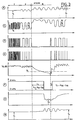
- fig. 3 illustrates signal shapes taken at different points in FIG. 2;
- fig. 4 illustrates the electrical diagram of an analog-digital conversion and affi chain improved digital chage according to the present invention;
- fig. 5, 6A and 6B illustrate the display members and the control keyboard, and
- fig. 7 illustrates the flow diagram of the operation of the chain of FIG. 4.
La fig. 1 illustre un montage classique de pesage en vue d'un affichage numérique. Le récepteur de charge (non représenté) possède par exemple la structure en anneau décrite dans la demande de brevet FR 2469701, munie de jauges de contraintes en tant que capteurs. Ces jauges de contraintes sont agencées en un pont 3, suivi d'un étage amplificateur 2, puis d'un filtre 1, dont la sortie est appliquée à un convertisseur analogique-numérique de poids 4 (fig. 4). Les filtres 1 utilisés jusqu'à présent comportent par exemple deux cellules R-C passe-bas en série.Fig. 1 illustrates a conventional weighing arrangement for digital display. The load receptor (not shown) has for example the ring structure described in patent application FR 2469701, fitted with strain gauges as sensors. These strain gauges are arranged in a
Des difficultés sont rencontrées en présence d'oscillations ou vibrations affectant soit le support de la balance, soit son plateau porte-charge et le corps à peser. Le cas des pèse-bébé est typique: un nouveau-né bouge beaucoup, à des fréquences relativement basses. Avec un filtre classique, le temps nécessaire pour filtrer suffisamment les fréquences tenant à ce mouvement dans le signal de pesage est pratiquement prohibitif.Difficulties are encountered in the presence of oscillations or vibrations affecting either the support of the balance, or its load-bearing plate and the body to be weighed. The case of baby scales is typical: a newborn baby moves a lot, at relatively low frequencies. With a conventional filter, the time necessary to sufficiently filter the frequencies due to this movement in the weighing signal is practically prohibitive.
Pour éviter ce temps d'attente à l'opérateur, il est connu de lui faire commander l'instant de mesure (par le convertisseur analogique-numérique) à l'aide d'un bouton-poussoir. La plupart du temps, la mesure est alors faite prématurément, et par conséquent entachée d'erreur. Enfin, cette erreur n'est pas négligeable, compte-tenu des faibles variations de poids qu'il est souhaitable de détecteur (mesure avant et après tétée, par exemple).To avoid this waiting time for the operator, it is known to make him control the measurement instant (by the analog-digital converter) using a push button. Most of the time, the measurement is then made prematurely, and therefore tainted with error. Finally, this error is not negligible, given the small variations in weight that it is desirable to detect (measurement before and after feeding, for example).
La présente invention vient proposer un filtre électronique perfectionné, que permet d'une manière générale l'obtention accélérée d'un signal de mesure débarrassé d'oscillations. Dans son application en pesage, ce filtre résoud le problème spécifique lié à la présence d'oscillations intempestives ou inéluctables, affectant le support de l'instrument de pesage et/ou le corps à peser.The present invention proposes an improved electronic filter, which generally allows accelerated obtaining of a measurement signal free of oscillations. In its application in weighing, this filter solves the specific problem linked to the presence of untimely or inevitable oscillations, affecting the support of the weighing instrument and / or the body to be weighed.
Ce filtre, illustré sur la fig. 2, va venir remplacer le bloc 1 de la fig. 1, du moins pour les applications de pesage.This filter, illustrated in fig. 2, will replace the
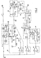
Sur la fig. 2, le filtre comporte une borne active d'entrée A, une borne active de sortie B, et bien entendu une masse, qui apparaissent également sur la fig. 1. Entre les bornes A et B et la masse est placé un quadripôle désigné généralement par 10, et constitué de deux éléments RC en série, le premier comprenant la résistance R12 suivie du condensateur C12 en parallèle sur la masse, et le second comprenant la résistance R13 suivie du condensateur C14 également en parallèle sur la masse.In fig. 2, the filter comprises an active input terminal A, an active output terminal B, and of course a ground, which also appear in FIG. 1. Between terminals A and B and ground is placed a quadrupole generally designated by 10, and consisting of two RC elements in series, the first comprising the resistor R12 followed by the capacitor C12 in parallel on the ground, and the second comprising the resistor R13 followed by capacitor C14 also in parallel on ground.
Selon la présente invention, il est prévu une maille à résistance commandée en parallèle sur la résistance R12. Cette maille à résistance commandée se compose ici d'une résistance R15, en série sur la maille source-drain d'un transistor à effet de champ Q16. Dans le mode de réalisation décrit, le transistor Q16 est du type métal-oxyde semiconducteur à grille isolée et à canal P.According to the present invention, there is provided a resistance mesh controlled in parallel on the resistor R12. This controlled resistance mesh consists here of a resistor R15, in series on the source-drain mesh of a field effect transistor Q16. In the embodiment described, the transistor Q16 is of the metal-oxide semiconductor type with insulated gate and with P channel.
A titre d'exemple particulier, dans le cas des pèse-bébé, les valeurs des résistances sont par exemple 2,2 mégohms pour R12, de 100 kilohms poùr R13, et de 5 kilohms pour R15. Les valeurs des capacités sont de 2,2 microfarads pour C12, et de 0,33 microfarads pour C14. Enfin, le transistor à effet de champ est par exemple le modèle J271 de la société «Siliconix» ou «National Semi-Con- ductor».As a particular example, in the case of baby scales, the resistance values are for example 2.2 megohms for R12, 100 kilohms for R13, and 5 kilohms for R15. The capacity values are 2.2 microfarads for C12, and 0.33 microfarads for C14. Finally, the field effect transistor is for example the J271 model from the company “Siliconix” or “National Semi-Conductor”.
On voit immédiatement que lorsque le transistor Q16 est bloqué, l'ensemble R12 et C12 correspond à une constante de temps de 4,84 s. A sa suite, l'ensemble R13 et C14 correspond à une constante de temps de 33 ms, assurant ainsi un filtrage complémentaire, notamment en raison des commutations imprimées à la première partie du filtre.We can immediately see that when transistor Q16 is blocked, the set R12 and C12 corresponds to a time constant of 4.84 s. Following this, the set R13 and C14 corresponds to a time constant of 33 ms, thus ensuring additional filtering, in particular because of the switches printed on the first part of the filter.
Au contraire, lorsque le transistor Q16 devient conducteur, c'est la résistance R15 qui devient rapidement prédominante, pour aboutir finalement à une constante de temps définie pratiquement par R15 et C12, et correspondant à 11 ms.On the contrary, when the transistor Q16 becomes conductive, it is the resistor R15 which quickly becomes predominant, finally leading to a time constant defined practically by R15 and C12, and corresponding to 11 ms.
La présente invention prévoit en outre une commande particulière de la variation de la constante de temps liée à la maille R15 Q16.The present invention further provides for a particular control of the variation of the time constant linked to the mesh R15 Q16.
Le signal présent sur la borne active d'entrée A est appliqué à trois étages formant amplificateur- tampon, notés respectivement 21, 35 et 36. Les étages 35 et 36 font partie de moyens discriminateurs, qui incorporent également les blocs 40, 50 et 60 de la fig. 2. Ces moyens discriminateurs sont sensibles au signal présent sur la borne A, pour fournir un signal de type créneau consécutivement à une variation de la composante continue du signal présent sur la borne active d'entrée A. Selon un aspect intéressant de l'invention, la durée de ce signal en créneau croît avec l'amplitude de la variation en question de la composante continue.The signal present on the active input terminal A is applied to three stages forming a buffer amplifier, noted respectively 21, 35 and 36. The
Plus précisément, les moyens discriminateurs comportent ici un étage amplificateur d'oscillations à fort gain, au moins dans les faibles signaux, référencé 40. Cet étage 40 est connecté à la borne d'entrée A par l'étage tampon 36. Il est suivi d'un comparateur 50, connecté par ailleurs à la borne d'entrée A à travers l'autre étage tampon 35. Enfin, un étage différentiateur 60 est connecté à la sortie de l'étage comparateur 50. En sortie du différentiateur 60, le signal en créneau précité est défini à partir de l'absence durable d'impulsions.More specifically, the discriminator means here comprise a high gain oscillation amplifier stage, at least in weak signals, referenced 40. This
On décrira maintenant plus en détail les éléments des blocs 40, 50 et 60 en référence à la fig. 2 ainsi qu'au diagramme de signaux de la fig. 3.The elements of
La ligne A de la fig. 3 représente un signal d'entrée supposé appliqué à la borne A. Pour bien faire apparaître les performances du filtre selon l'invention, ce signal se compose d'une première partie I, constituée d'une tension rigoureusement constante de valeur V, et débarrassée d'oscillations. Ensuite, dans une partie II, une oscillation de basse fréquence est superposée au signal continu Vl. Dans la partie III, la composante continue en valeur moyenne du signal augmente, pour passer à une valeur V2, tout en continuant à être animée de sur-oscillations.Line A of fig. 3 represents an input signal assumed to be applied to terminal A. To clearly show the performance of the filter according to the invention, this signal consists of a first part I, consisting of a strictly constant voltage of value V, and free of oscillations. Then, in part II, a low frequency oscillation is superimposed on the continuous signal V l . In Part III, the continuous component in mean value of the signal increases, to pass to a value V 2 , while continuing to be animated by over-oscillations.
Sur la fig. 2, le bloc 40 est constitué d'un amplificateur différentiel hacheur à très haute impédance d'entrée, noté 41. Cet amplificateur est par exemple le modèle ICL 7650CPD, vendu par la société «Intersil». Cet amplificateur possède normalement un gain en boucle ouverte de l'ordre de 106, et une impédance d'entrée de l'ordre de 1010 ohms. De manière connue, il est muni de deux capacités auxiliaires notées C45 sur la fig. 2.In fig. 2, block 40 consists of a differential chopper amplifier with very high input impedance, noted 41. This amplifier is for example the ICL 7650CPD model, sold by the company "Intersil". This amplifier normally has an open loop gain of the order of 10 6 , and an input impedance of the order of 10 10 ohms. In known manner, it is provided with two auxiliary capacities denoted C45 in FIG. 2.
L'entrée non inverseuse de l'amplificateur 41 est reliée à la borne A par l'intermédiaire de l'étage tampon 36, à travers une résistance série R43, valant par exemple 2,2 mégohms, et suivie d'une capacité parallèle C44, valant par exemple 330 nanofarads. On observera que cela correspond à une constante de temps d'environ 0,73 s.The non-inverting input of the
L'entrée inverseuse de l'amplificateur 41 est reliée à la sortie de l'étage 36 par une résistance R42 mesurant par exemple 4,7 kilohms. Cette même entrée inverseuse est reliée à la sortie de l'amplificateur 41 par une contre-réaction non linéaire à diodes, comprenant deux diodes D46 en série dans un sens, et deux diodes D47 en série dans l'autre sens. Ces diodes sont de préférence des diodes au silicium tel que le modèle 1 N4148.The inverting input of the
L'étage 40 ainsi monté présente la propriété d'avoir un gain pratiquement unité pour les signaux d'entrée continus. En effet, l'impédance de l'entrée non inverseuse aussi bien que de l'entrée inverseuse est très grande même par rapport à la résistance interne des diodes D46 et D47. De plus, le courant qui traversera les résistances R42 et R43 de même que les diodes D46 et D47 sera également très faible compte tenu de l'impédance d'entrée de l'amplificateur 41. En courant continu, les deux entrées de l'amplificateur étant au même potentiel la sortie suit les entrées.The
Dès que le signal d'entrée atteint des fréquences dépassant le seuil qui correspond à la constante de temps de 0,73 s associée au groupe R43 C44, les choses se passent différemment. On notera que cette fréquence de seuil est de l'ordre de 0,2 Hertz, sous réserve des effets dus au grand gain de l'amplificateur, à sa contreréaction linéaire, et aux autres résistances intervenant.As soon as the input signal reaches frequencies exceeding the threshold which corresponds to the time constant of 0.73 s associated with the group R43 C44, things happen differently. It will be noted that this threshold frequency is of the order of 0.2 Hertz, subject to the effects due to the large gain of the amplifier, to its linear counteraction, and to the other resistances involved.
Lorsqu'on approche de cette fréquence de seuil, il se produit d'une part un déphasage et d'autre part une atténuation de l'entrée non inverseuse de l'amplificateur 41 par rapport à son entrée inverseuse. Très rapidement, le gain de l'amplificateur intervient, ce qui fait changer d'état sa sortie. Les diodes D46 et D47 empêchent le passage de ladite sortie en saturation, et limitent la différence de tension entre la sortie et l'entrée inverseuse à ± 1,2 V. Compte-tenu du gain de 106 de l'amplificateur 41 en boucle ouverte, cela correspond à une différence de tension de 1,2 RV entre les deux entrées de cet amplificateur. Ce qui précède est valable pour les faibles amplitudes de signaux dépassant la fréquence de coupure. Lorsque l'amplitude du signal devient forte, la contre-réaction produite par les diodes D46 et D47 augmente, d'où il résulte une diminution rapide du gain de l'étage amplificateur.When approaching this threshold frequency, there is on the one hand a phase shift and on the other hand an attenuation of the non-inverting input of the
On examinera maintenant la ligne C de la fig. 3. Pendant la partie du signal A, l'entrée de l'amplificateur 41 ne voit que des bruits de fréquence élevée (non représentés sur la ligne A). De fréquence assez élevée, ce bruit est fortement amplifié, pour donner une amplitude crête à crête de 2,4 V, au-dessus d'un seuil minimum de tension égal à V4. Dans la partie Il du signal A, la sortie de l'amplificateur 41 est un signal à la même fréquence que l'oscillation, mais fortement amplifiée, c'est-à-dire qu'il présente des fronts de montée et de descente très nets, suivis de paliers arrondis compte tenu de la chute du gain de l'amplificateur 41 lorsque sa tension de sortie atteint les seuils définis par les diodes D46 et D47. L'amplitude crête à crête notée V3 est là encore égale à environ 2,4 V. La valeur moyenne de ce signal est la même que pendant la phase I.We will now examine line C in fig. 3. During the part of signal A, the input of
Au début de la phase III du signal A, la valeur de la composante continue de ce signal augmente, passant de V, à V2. On a déjà indiqué que l'étage amplificateur 40 possède un gain unité pour des tensions continues. En conséquence, la valeur de la tension monte sur le diagramme C de la fig. 3, pour reprendre progressivement des oscillations d'amplitude croissante, qui finiront par atteindre en partie droite la même amplitude crête à crête V3 que précédemment. La réapparition progressive des oscillations tient à l'effet combiné de la contre-réaction non linéaire à seuil des diodes D46 et D47 sur l'amplificateur, et du réseau RC présent sur son entrée non inverseuse. On remarque que le retour des oscillations à leur amplitude crête à crête V3 prendra d'autant plus de temps que la variation de la composante continue du signal présent sur l'entrée A est plus importante.At the start of phase III of signal A, the value of the DC component of this signal increases, going from V, to V 2 . It has already been indicated that the
L'étage amplificateur d'oscillations à fort gain 40 est suivi d'un étage comparateur 50, la sortie de l'amplificateur 41 étant reliée à l'entrée inverseuse du comparateur 51. L'entrée non inverseuse de ce même comparateur est reliée d'une part à la sortie de l'étage tampon 35 par une résistance R52, et d'autre part à la sortie du comparateur 51 par une résistance R53. La résistance R53 est nettement plus grande que la résistance R52, typiquement d'un facteur 500 environ, ce qui donne à ce comparateur 51 un fonctionnement à faible hystérésis.The high gain
L'étage comparateur 50 va donc comparer le signal d'entrée A au signal au point C, représentés sur les deux premiers diagrammes de la fig. 3. Pendant la phase I, l'amplitude crête à crête en sortie au point C est importante, ce qui va produire un passage alterné très rapide de la sortie de l'étage comparateur 50 entre ces deux tensions extrêmes. Cela se fait à la fréquence du bruit donc à une fréquence très grande. Ensuite, pendant la phase II, les choses se passent de même, mais à la fréquence des oscillations surimposées à la composante continue du signal A. On obtient donc un signal rectangulaire. Au début de la phase III, le signal au point C demeure en permanence supérieur au signal d'entrée A. Comme le signal au point C est appliqué sur l'entrée inverseuse du comparateur 51, celui-ci demeure en permanence avec une sortie au niveau bas. Au bout d'un certain temps, lié à la vitesse de réapparition des oscillations au point C, le signal au point A devient à nouveau supérieur par moments au signal au point C. Cela commence, dans l'exemple représenté où la composante continue a augmenté, par un dépassement qui s'effectue sur les alternances négatives du signal A. On voit donc apparaître au point D, comme le montre le troisième diagramme de la fig. 3, des impulsions qui apparaissent à chaque alternance négative du signal A, et ont une durée progressivement croissante jusqu'à atteindre tout la durée de l'alternance négative. Le régime permanent que l'on atteint ensuite est le même que ce qui existait au point D pendant la phase Il.The
Le signal D est ensuite appliqué à un étage différentiateur 60, connecté à la sortie de l'étage comparateur 50.The signal D is then applied to a
Dans le mode de réalisation représenté, l'étage différentiateur 60 est constitué à partir d'une porte OU EXCLUSIF 61, dont une entrée reçoit directement la sortie de l'étage 50, tandis que l'autre reçoit la même sortie à travers un réseau RC constitué de la résistance série R62 et du condensateur C63 en parallèle vers la masse. Ce réseau RC va produire un déphasage entre les deux entrées de la porte 61. En conséquence, toute transition rapide apparaissant dans le signal D va se traduire par l'apparition d'une impulsion sur le signal E disponible en sortie de la porte 61. Ce signal E est illustré sur le diagramme E de la fig. 3. Il comporte de multiples impulsions rapprochées en regard de la partie du signal A. En regard de la partie II, il comporte des impulsions sensiblement au niveau de chaque passage par zéro du signal A. Au début de la partie III, aucune impulsion n'apparaît. Les impulsions réapparaissent lorsque le signal D réapparaît lui aussi. Ces impulsions sont au début deux impulsions rapprochées, séparées d'un intervalle de temps un peu plus large des deux impulsions rapprochées suivantes. Et au fur et à mesure que l'on recouvre le régime stationnaire avec une amplitude crête à crête V3 dans le signal C, les impulsions du signal E deviennent à nouveau régulièrement réparties dans le temps.In the embodiment shown, the differentiating
Le signal-créneau précédemment mentionné est défini à partir de l'absence durable d'impulsions dans le signal E, c'est-à-dire en sortie de l'étage différentiateur. On a observé précédemment que le retour du signal C à son amplitude crête à crête normale V3 est d'autant plus long que la variation de la composante continue du signal A est plus importante. Corrélativement, la durée du signal-créneau présent dans le signal E est elle aussi d'autant plus longue que la variation de la composante continue est plus importante.The previously mentioned slot signal is defined from the lasting absence of pulses in signal E, that is to say at the output of the differentiating stage. It has been observed previously that the return of signal C to its normal peak-to-peak amplitude V3 is all the longer as the variation of the DC component of signal A is greater. Correlatively, the duration of the slot signal present in the signal E is also all the longer as the variation of the DC component is greater.
Le signal E est appliqué à un étage amplificateur intermédiaire 70, constitué ici de deux portes OU EXCLUSIF 71 et 72 branchées en parallèle. L'une des entrées de chaque porte reçoit le signal E, l'autre recevant la masse. L'homme de l'art comprendra que la sortie de l'étage 70 reproduit la forme du signal E, mais avec une énergie plus grande.The signal E is applied to an
Après cet étage amplificateur.70, le signal E se trouve donc appliqué au circuit monostable réarmable 80. Dans le mode de réalisation représenté, ce circuit monostable réarmable est fondé sur un condensateur C85, monté en parallèle sur une résistance R83, l'une des bornes de cet ensemble étant reliée à la masse. La borne opposée du même ensemble est reliée par une résistance R84 à la cathode d'une diode D82 dont l'anode reçoit la sortie de l'étage 70. Enfin, le point chaud commun à la capacité C85 et aux résistances R83 et R84 est relié à une entrée d'une porte OU EXCLUSIF 81 dont l'autre entrée est reliée à la masse. La capacité du condensateur C85 est par exemple égale à 1 microfarad, tandis que les valeurs des résistances R83 et R84 sont très différentes, la résistance R84 valant par exemple 4,7 kilohms, tandis que la résistance R84 vaut 1 mégohm. Il en résulte que la sortie de l'étage 70 va charger le condensateur C85 avec une constante de temps rapide, dépendant essentiellement de la résistance R84, alors que ce même condensateur va se décharger avec une constante de temps lente, dépendant essentiellement de la résistance R83.After this amplifier stage. 70, the signal E is therefore applied to the resettable
Les impulsions rapprochées des phases 1 et Il du signal A vont donc se traduire par une charge répétée du condensateur C85, d'où le fonctionnement de celui-ci en étage monostable réarmable. En revanche, lorsque ces impulsions disparaissent au début de la phase III, le condensateur C85 va se décharger lentement, comme le montre le diagramme VC85 de la fig. 3. Lorsque la tension aux bornes du condensateur atteint la valeur de basculement Vo de la porte 81, le signal F disponible en sortie de cette porte change d'état en passant d'un niveau élevé à un niveau bas.The close pulses of
Cela se produit au bout d'un intervalle de temps T1 qui est lié essentiellement à la constante de temps R83xC85. On voit bien que le circuit monostable réarmable 80 définit un intervalle de temps neutre, de durée prédéterminée Tl, consécutivement au début du signal-créneau.This occurs at the end of a time interval T 1 which is essentially linked to the time constant R83xC85. It can be seen that the resettable
A la fin du signal-créneau, ou peu après celle-ci, le signal au point F va retourner à sa valeur maximum. En effet, la première impulsion qui réapparaît dans le signal E est la plupart du temps insuffisante pour recharger assez le condensateur C85 de manière à dépasser de façon détectable la tension Vo, et à faire basculer la porte 81. En revanche, cela se produira au niveau de la deuxième impulsion, ou éventuellement au niveau d'une impulsion suivante. Le diagramme F de la fig. 3 admet que ce basculement se produit au niveau de la deuxième impulsion, donc avec un retard T2 par rapport à la première impulsion et à la fin du signal-créneau. Ce retard est lié principalement à la valeur de la constante de temps définie par le produit R84xC85.At the end of the slot signal, or shortly thereafter, the signal at point F will return to its maximum value. Indeed, the first pulse which reappears in the signal E is most of the time insufficient to sufficiently recharge the capacitor C85 so as to detectably exceed the voltage V o , and to toggle the
Selon un aspect particulier de la présente invention, la durée de l'intervalle de temps neutre est choisie au moins égale à la valeur de la demi- période correspondant à la fréquence la plus basse que l'on désire filtrer. Par exemple, si la fréquence limite à filtrer est de 1 Hz, la durée de l'intervalle de temps neutre est au moins égale à 0,5s.According to a particular aspect of the present invention, the duration of the neutral time interval is chosen at least equal to the value of the half-period corresponding to the lowest frequency which it is desired to filter. For example, if the limit frequency to be filtered is 1 Hz, the duration of the neutral time interval is at least equal to 0.5 s.
L'intervalle de temps T2 n'est pas critique, il peut être cependant avantageusement aussi court que possible. Une façon de faire consiste à utiliser un circuit intégré formant monostable réarmable, plutôt que la réalisation détaillée de l'étage 80 telle qu'elle apparaît sur la fig. 2.The time interval T 2 is not critical, it can however advantageously be as short as possible. One way of doing this is to use an integrated circuit forming a resettable monostable, rather than the detailed embodiment of
Pendant l'intervalle de temps neutre de durée T" la variation de la composante continue intervenant dans le signal A au début de la phase III va donc avoir le temps de s'établir complètement. Cette composante continue restera donc sensiblement stationnaire dans la suite.During the neutral time interval of duration T ", the variation of the continuous component intervening in the signal A at the start of phase III will therefore have time to settle down completely. This continuous component will therefore remain substantially stationary in the following.
On observera encore que le signal F est constitué par la sortie d'une porte logique, et varie donc entre une valeur supérieure d'environ 8 V et une valeur inférieure proche de 0 V.It will also be observed that the signal F consists of the output of a logic gate, and therefore varies between a higher value of approximately 8 V and a lower value close to 0 V.
Le signal F disponible en sortie de l'étage monostable 80 est appliqué d'une part à la cathode d'une diode D29 dont l'anode est reliée à une résistance R28, qui à son tour est reliée au point Q. Le point F est également relié directement au point Q à travers une résistance R27 de valeur nettement supérieure à celle de R28. Par exemple, la résistance R27 vaut 270 kilohms, tandis que la résistance R28 vaut 12 kilohms. Le point Q est relié par une résistance R26 mesurant par exemple 47 kilohms la grille du transistor à effet du champ Q16. Le même point Q est relié d'une part à l'armature positive d'un condensateur électrochimique C23 dont l'armature négative est reliée par une résistance R25 à la tension de +8 V constituant l'alimentation. Le point Q est relié d'autre part à la cathode d'une diode D24 dont l'anode est reliée elle aussi au point P formant le point commun entre le pôle négatif du condensateur C23 et la résistance R25. Enfin, ce même point P est relié à l'anode d'une diode D22 dont la cathode va vers la sortie de l'étage amplificateur tampon 21 déjà mentionné, qui possède un gain 1 et dont l'entrée non inverseuse est comme pour les autres amplificateurs tampons reliée au point A.The signal F available at the output of the
Pendant les phases I et Il du signal au point A, le signal F est en régime stationnaire à la valeur de +8 V. Cette tension est reportée au point Q à travers la résistance R27. Elle apparaît donc sur l'armature positive du condensateur C23. Le point P, ou armature négative du condensateur C23, suit la tension présente au point A, augmentée de la valeur de la tension de seuil de la diode D22, soit environ 0,6 V, s'agissant d'une diode au silicium. Le condensateur C23 est donc chargé sensiblement suivant la différence entre la tension présente au point F et la tension présente au point A (sauf les 0,6 V de la diode D22, et le fait que le signal au point F est légèrement inférieur à 8 V). Cette tension au point Q se trouve donc appliquée à la grille isolée du transistor Q16, qui est bloqué et présente donc une très forte impédance entre la résistance R15 et le point commun de la résistance R12 et du condensateur C12.During phases I and II of the signal at point A, the signal F is in steady state at the value of +8 V. This voltage is transferred to point Q through the resistor R27. It therefore appears on the positive armature of capacitor C23. The point P, or negative armature of the capacitor C23, follows the voltage present at point A, increased by the value of the threshold voltage of the diode D22, that is to say about 0.6 V, in the case of a silicon diode. The capacitor C23 is therefore charged substantially according to the difference between the voltage present at point F and the voltage present at point A (except the 0.6 V of the diode D22, and the fact that the signal at point F is slightly less than 8 V). This voltage at point Q is therefore applied to the isolated gate of transistor Q16, which is blocked and therefore has a very high impedance between the resistor R15 and the common point of the resistor R12 and of the capacitor C12.
Les propriétés de filtrage du quadripôle 10 sont alors uniquement définies par la résistance R12 et le condensateur C12 pour sa première section, et par la résistance R13 et le condensateur C14 pour sa deuxième section. Compte tenu des valeurs numériques précédemment données, c'est le réseau R12 C12 qui prédomine, et définit une constante de temps de l'ordre de 5 s (le produit vaut exactement 4,84 s). Le diagramme G de la fig. 3 illustre que pendant l'intervalle de temps Ti, pour lequel le signal F demeure à environ +8 V, au début de la phase III, le transistor Q16 demeure bloqué. Dans ces conditions, le signal B qui représente la sortie du quadripôle filtrant va augmenter très légèrement, commençant à suivre la variation de la composante continue du signal A, mais avec une très grande «inertie».The filtering properties of the
Au terme de l'intervalle de temps T" le signal F change d'état, passant brutalement à une valeur proche de zéro. Le condensateur C23 de l'étage 20 se décharge alors brutalement à travers la résistance R28 et la diode D29. Très rapidement, le transistor Q16 devient conducteur, et c'est alors la résistance R15 qui définit avec le condensateur C12 la constante de temps du quadripôle 1 dans sa première section. Comme précédemment indiqué, cette constante de temps est de 11 ms. Des oscillations apparaissent immédiatement en sortie sur le signal B. Ces oscillations acquièrent rapidement une amplitude et une valeur moyenne conformes à celles du signal A. Cet état de choses dure jusqu'à ce que le signal F remonte à +8 V.At the end of the time interval T "the signal F changes state, suddenly passing to a value close to zero. The capacitor C23 of
On observera au passage que pendant le niveau bas du signal F, la tension au point G, sur la grille du transistor Q16, est maintenue, dans sa composante continue, très proche de la tension au point A. En effet, la tension au point G est définie par la fin de la décharge du condensateur C23, à travers la résistance R28 et la diode D29. Cependant, la tension de +8 V est appliquée à travers la résistance R25, pour venir maintenant dans le sens conducteur à travers la diode D24. Si l'on se ra- pelle que la tension au point P est égale à la tension au point A moins le seuil de 0,6 V de la diode D22, il apparaît immédiatement que la tension au point Q serait égale à la tension au point P plus la même tension de seuil de 0,6 V provoquée par la diode D24. En conséquence, il apparaît que la tension existant au point Q suit fidèlement la tension au point A du moins dans sa composante continue. Comme le montre le signal G en regard de la partie basse du signal F, des variations alternatives de faible amplitude apparaissent également. Cette caractéristique, quoi que non strictement nécessaire, s'est avérée très intéressante pour le bon fonctionnement du dispositif de la présente invention, du moins avec un transistor à effet de champ du type utilisé ici.It will be observed in passing that during the low level of the signal F, the voltage at point G, on the gate of transistor Q16, is maintained, in its DC component, very close to the voltage at point A. Indeed, the voltage at point G is defined by the end of the discharge of the capacitor C23, through the resistor R28 and the diode D29. However, the voltage of +8 V is applied through the resistor R25, to now come in the conductive direction through the diode D24. If we remember that the voltage at point P is equal to the voltage at point A minus the 0.6 V threshold of diode D22, it immediately appears that the voltage at point Q would be equal to the voltage at point P plus the same threshold voltage of 0.6 V caused by diode D24. Consequently, it appears that the voltage existing at point Q faithfully follows the voltage at point A at least in its DC component. As signal G shows next to the lower part of signal F, alternative variations of low amplitude also appear. This characteristic, although not strictly necessary, has proved to be very advantageous for the proper functioning of the device of the present invention, at least with a field effect transistor of the type used here.
On se replace maintenant au point où le signal F retourne à +8 V. La diode D29 est naturellement bloquée. Et la recharge du condensateur C23 va se produire à travers la résistance R27. Cette résistance étant la plus importante au niveau de l'étage 20, c'est essentiellement le produit de la valeur de la résistance R27 par la capacité du condensateur C23 qui va définir la constante de temps de recharge de ce dernier. Typiquement, cette constante de temps est de l'ordre de 3 s (le produit R27.C23 s'élève exactement à 2,7 s). La tension au point G va donc remonter très progressivement jusqu'à la valeur de +8 V. Il en résulte un retour progressif du transistor Q16 à l'état bloqué, et par conséquent une transition des propriétés de filtrage du quadripôle 10 entre la constante de temps R15xC12 et la constante de temps beaucoup plus importante R12xC12. Comme précédemment indiqué, la constante de temps R27xC23 est choisie, compte tenu de la caractéristique de réponse du transistor Q16, de sorte que la pente de variation de la constante de temps du quadripôle filtrant demeure inférieure à la fréquence minimale à filtrer.We now go back to the point where the signal F returns to +8 V. The diode D29 is naturally blocked. And the recharging of the capacitor C23 will occur through the resistor R27. This resistance being the most important at the level of
De cette augmentation de la constante de temps, il résulte selon le diagramme B de la fig. 3 une atténuation rapide des oscillations présentes sur le signal B, qui atteint alors rapidement la valeur V2 correspondant à la nouvelle valeur de la composante continue du signal d'entrée A, au niveau de la phase III.From this increase in the time constant, it results according to diagram B of FIG. 3 a rapid attenuation of the oscillations present on the signal B, which then quickly reaches the value V 2 corresponding to the new value of the DC component of the input signal A, at the level of phase III.
Des essais ont été effectués avec un instrument de pesage possédant 2000 points de mesure pour une portée maximale de 10 kg, c'est-à-dire une résolution de 5 g à l'affichage numérique. Le plateau de la balance a été soumis à une vibration à la fréquence de 1 Hz, avec une amplitude de ± 100 échelons, soit ± 500 g. Un poids de valeur connue a été ensuite placé sur le plateau. La valeur exacte de ce poids a été obtenue en 7 s.Tests were carried out with a weighing instrument having 2000 measurement points for a maximum range of 10 kg, that is to say a resolution of 5 g on the digital display. The balance pan was subjected to a vibration at the frequency of 1 Hz, with an amplitude of ± 100 steps, ie ± 500 g. A weight of known value was then placed on the pan. The exact value of this weight was obtained in 7 s.
A titre comparatif, la même constante de temps de régime permanent, sans filtrage selon la présente invention serait obtenue en enlevant la résistance R15 et le transistor Q16, c'est-à-dire à partir de la constante de temps définie par R12 et C12, qui est de 4,84 s. Pour obtenir à coup sûr une atténuation suffisante compte tenu des 2000 points de mesure, il faut attendre au moins 7,6 fois cette constante de temps. Cela conduit à un temps d'attente proche de 40 s. Comme précédemment indiqué, une telle attente est généralement trop longue pour l'opérateur, ce qui a conduit dans certains cas à prévoir un bouton-poussoir pour commander la mesure de façon anticipée, d'où il résulte que cette mesure est entachée d'une erreur non négligable.By way of comparison, the same steady-state time constant, without filtering according to the present invention, would be obtained by removing the resistor R15 and the transistor Q16, that is to say from the time constant defined by R12 and C12 , which is 4.84 s. In order to obtain sufficient attenuation for sure taking into account the 2000 measurement points, it is necessary to wait at least 7.6 times this time constant. This leads to a waiting time close to 40 s. As previously indicated, such a wait is generally too long for the operator, which has led in some cases to provide a push button for ordering the measurement in advance, from which it follows that this measurement is marred by a significant error.
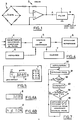
La chaîne de mesure selon la présente invention est obtenue de la manière suivante: on remplace le filtre 1 de la fig. 1 par le filtre selon l'invention illustré sur la fig. 2, et la sortie de ce filtre est appliquée au convertisseur analogique-numérique de poids 4 de la fig. 4. La grande précision obtenue, dans un temps raisonnable, permet d'envisager des mesures différentielles faibles. A cet effet, au lieu d'être relié directement à l'affichage numérique 8, le convertisseur 4 est relié à une logique de commande, interconnectée de son côté avec des mémoires 6 et un clavier 7, et pilotant l'affichage numérique 8.The measuring chain according to the present invention is obtained in the following manner: the
Le clavier 7 et l'affichage numérique 8 sont illustrés sur la fig. 5, qui représente par exemple la face avant d'un pèse-bébé. Le clavier 7 comprend les chiffres numériques classiques, plus une commande C permettant une correction, et un retour à l'affichage du poids, et une touche E permettant l'enregistrement du poids. L'affichage numérique 8 comporte à droite 4 chiffres.significatifs pour l'affichage du poids de 0 à 10 kg par tranche de 5g. De manière connue, un point décimal indique que le zéro de pesage est correct. A gauche de ce point décimal, il est prévu une zone d'affichage supplémentaire qui permet d'afficher une information d'adresse telle qu'un numéro de lit, cette information étant introduite au niveau du clavier 7 de la manière décrite plus loin.The
La logique de commande 5 sera maintenant décrite en référence à l'algorithme de la fig. 7. Après la première étape d'initialisation 90, le régime normal consiste à afficher le poids à l'étape 91. L'affichage présente alors la forme de la fig. 6A, dans l'hypothèse d'un poids de 3285 g. Ensuite, le test 92 examine si l'opérateur a actionné la touche E. Si non, on continue à afficher le poids. Si oui, on passe à l'affichage de E au niveau de l'emplacement d'adresse sur l'affichage 8. La logique est alors en attente de l'introduction du numéro de lit, ou de l'adresse, par l'opérateur à l'aide du clavier 7. On suppose ici que l'opérateur introduit le numéro de lit ou adresse 4. Si aucun numéro de lit n'est introduit, la logique peut rester en attente, ou de préférence retourner à l'affichage du poids en 91, au bout d'un temps prédéterminé égal par exemple à une minute. Si un numéro de lit est introduit, l'étape 95 consiste alors à afficher le numéro de lit au niveau de l'affichage (fig. 6B). L'affichage est complété par la lettre «d», indiquant que le reste de l'affichage va être une différence de poids. La logique de commande 5 effectue alors la différence entre le nouveau poids et l'ancien poids disponible dans la mémoire 6 à l'adresse 4. On suppose ici que cette différence est égale à 104 g, et elle est donc affichée comme le montre a fig. 6B. En même temps, la logique de commande substitue dans la mémoire 6, et à l'adresse 4, la nouvelle valeur de poids soit 3285 g. On retourne ensuite au régime normal qui est l'affichage du poids en 91.The
Cette disposition est très intéressante notamment pour la surveillance des bébés en hôpital. Un ou plusieurs bébés sont pesés avant la tétée, leur poids étant mémorisé dans l'appareil. Une seconde pesée faite après leur alimentation permet à la balance de calculer par différence l'accroissement de poids du bébé. Dix mémoires par exemple sont prévus, portant les numéros 0 à 9, ce nombre n'étant naturellement pas limitatif.This provision is very interesting especially for monitoring babies in hospitals. One or more babies are weighed before feeding, their weight being stored in the device. A second weighing made after feeding allows the scale to calculate the difference in the baby's weight difference. Ten memories for example are provided, bearing the
La description détaillée qui précède montre que la présente invention s'applique particulièrement bien au cas des pèse-bébé, mais elle n'est pas limitée à cette application, et peut également servir au pesage d'animaux, ainsi qu'à tout autre pesage où le plateau se trouve animé d'oscillations parasites. Inversement, l'invention peut également servir lorsque c'est non pas le plateau mais le support de la balance qui est animé d'oscillations, comme c'est le cas par exemple lors d'un pesage en camion de livraison.The foregoing detailed description shows that the present invention applies particularly well to the case of baby scales, but it is not limited to this application, and can also be used for weighing animals, as well as for any other weighing where the plate is animated by parasitic oscillations. Conversely, the invention can also be used when it is not the pan but the support of the balance which is animated by oscillations, as is the case for example during weighing in a delivery truck.
Bien entendu, la présente invention n'est pas limitée au mode de réalisation décrit, mais s'étend à toute variante incluse dans le cadre des revendications ci-après. On pourra en particulier remplacer les circuits 10, 20, 40, 50, 60, 70 et 80 par tous moyens équivalents.Of course, the present invention is not limited to the embodiment described, but extends to any variant included within the scope of the claims below. In particular,
Claims (10)
Applications Claiming Priority (2)
| Application Number | Priority Date | Filing Date | Title |
|---|---|---|---|
| FR8220201A FR2537276A1 (en) | 1982-12-02 | 1982-12-02 | ELECTRONIC MEASURING DEVICE WITH ACCELERATED LOW-PASS FILTERING, PARTICULARLY FOR WEIGHING |
| FR8220201 | 1982-12-02 |
Publications (2)
| Publication Number | Publication Date |
|---|---|
| EP0112218A1 EP0112218A1 (en) | 1984-06-27 |
| EP0112218B1 true EP0112218B1 (en) | 1986-11-20 |
Family
ID=9279717
Family Applications (1)
| Application Number | Title | Priority Date | Filing Date |
|---|---|---|---|
| EP83402278A Expired EP0112218B1 (en) | 1982-12-02 | 1983-11-25 | Electronic measuring device with accelerated low-pass filtering, particularly for weighing |
Country Status (5)
| Country | Link |
|---|---|
| US (1) | US4531600A (en) |
| EP (1) | EP0112218B1 (en) |
| CA (1) | CA1191613A (en) |
| DE (1) | DE3367810D1 (en) |
| FR (1) | FR2537276A1 (en) |
Families Citing this family (12)
| Publication number | Priority date | Publication date | Assignee | Title |
|---|---|---|---|---|
| DE3479237D1 (en) * | 1983-04-14 | 1989-09-07 | Ishida Scale Mfg Co Ltd | Weighing apparatus |
| JPS60228926A (en) * | 1984-04-26 | 1985-11-14 | Tokyo Electric Co Ltd | Electronic charge scale with label printer |
| GB2173308B (en) * | 1985-04-02 | 1988-12-29 | Shinko Denshi Kk | Weight measuring apparatus of vibration type |
| US4705126A (en) * | 1985-09-24 | 1987-11-10 | Ishida Scales Manufacturing Company, Ltd. | Signal processing circuit and weighing apparatus incorporating same |
| US4696359A (en) * | 1986-08-22 | 1987-09-29 | National Transducer Corporation | Electronic weighing apparatus |
| US4967384A (en) * | 1988-03-14 | 1990-10-30 | General Electrodynamics Corporation | Highly accurate weighing system |
| US4909340A (en) * | 1989-02-03 | 1990-03-20 | John Chatillon & Sons Inc. | Electronic weighing scale |
| US4991446A (en) * | 1989-10-05 | 1991-02-12 | Metriguard, Inc. | Force measurement with compensation of errors caused by accelerations of measuring apparatus |
| US5131482A (en) * | 1989-12-28 | 1992-07-21 | General Electrodynamics | Self-contained weighing system and method |
| WO2008041490A1 (en) * | 2006-09-27 | 2008-04-10 | Shimadzu Corporation | Electronic balance |
| CN100489466C (en) * | 2007-08-10 | 2009-05-20 | 中国航天科技集团公司第四研究院第四十四研究所 | Self-adaptive filtering method of dynamic axle weighing signal of vehicle |
| CN103424167B (en) * | 2012-05-21 | 2016-08-03 | 梅特勒-托利多(常州)测量技术有限公司 | Utilize the method that car load measurement vehicle weighing apparatus calculates axle weight |
Family Cites Families (9)
| Publication number | Priority date | Publication date | Assignee | Title |
|---|---|---|---|---|
| US3525991A (en) * | 1966-06-15 | 1970-08-25 | Toledo Scale Corp | Converter |
| US3434343A (en) * | 1967-04-03 | 1969-03-25 | Blh Electronics | Low frequency damping circuit for strain gage transducers |
| GB1407195A (en) * | 1971-10-21 | 1975-09-24 | Barton M | Electronic weighing apparatus |
| DE2205778A1 (en) * | 1972-02-08 | 1973-08-16 | Boekels & Co H | CIRCUIT ARRANGEMENT FOR USE ON ELECTRIC TRANSDUCERS, IN PARTICULAR ELECTRO-MECHANICAL SCALES |
| GB1356069A (en) * | 1972-04-11 | 1974-06-12 | Autopack Ltd | Weighing machines |
| US4045731A (en) * | 1974-11-21 | 1977-08-30 | Takeda Riken Kogyo Kabushikikaisha | Filter having an automatically controlled variable cut-off frequency |
| DE2537560A1 (en) * | 1975-08-22 | 1977-03-03 | Sartorius Werke Gmbh | PROCEDURE AND CIRCUIT ARRANGEMENT FOR THE PROCESSING OF DC SIGNALS WITH ELECTRIC TRANSDUCERS, IN PARTICULAR ELECTROMECHANICAL PRECISION AND FINE SCALES |
| SE393188B (en) * | 1975-08-28 | 1977-05-02 | Asea Ab | WEIGHING EQUIPMENT |
| FR2323131A1 (en) * | 1975-09-02 | 1977-04-01 | Deze Cie Fse Mines | Weighing machine for moving objects - has low pass filter strongly attenuating resonant frequency of transducer loaded with nominal weight |
-
1982
- 1982-12-02 FR FR8220201A patent/FR2537276A1/en active Granted
-
1983
- 1983-11-25 DE DE8383402278T patent/DE3367810D1/en not_active Expired
- 1983-11-25 EP EP83402278A patent/EP0112218B1/en not_active Expired
- 1983-11-30 US US06/556,316 patent/US4531600A/en not_active Expired - Fee Related
- 1983-11-30 CA CA000442292A patent/CA1191613A/en not_active Expired
Also Published As
| Publication number | Publication date |
|---|---|
| DE3367810D1 (en) | 1987-01-08 |
| CA1191613A (en) | 1985-08-06 |
| FR2537276A1 (en) | 1984-06-08 |
| US4531600A (en) | 1985-07-30 |
| EP0112218A1 (en) | 1984-06-27 |
| FR2537276B1 (en) | 1985-05-03 |
Similar Documents
| Publication | Publication Date | Title |
|---|---|---|
| EP0112218B1 (en) | Electronic measuring device with accelerated low-pass filtering, particularly for weighing | |
| EP2966454B1 (en) | Method for measuring a physical parameter, and electronic circuit for implementing same | |
| EP0285478B1 (en) | Circuit for converting analogous signals into digital signals | |
| EP0018858B1 (en) | Process and device for calculating and adjusting the optimum value of ignition timing | |
| EP0674247B1 (en) | Clock with manual control | |
| EP0007288B1 (en) | Arrangement for measuring the intensity of a force which is transversally exerted on the free end of a flexion beam | |
| EP2131494B1 (en) | Circuit with switched capacitances with reduced consumption | |
| EP0137093B1 (en) | Method of measuring the voltage induced in the coil of a stepping motor by the rotation of its rotor | |
| EP2618164A1 (en) | Method for measuring a physical parameter and electronic circuit to interface with a capacitive sensor for implementing same | |
| CA1221416A (en) | Very weak electric resistance measuring ohmmeter | |
| CH690936A5 (en) | Ultrasonic detection device, in particular for an automatically controlled windshield cleaning system. | |
| EP0033705A2 (en) | Capacitance measuring device for a weighing apparatus | |
| EP2327160A1 (en) | Analog counter, and imager incorporating such a counter | |
| EP0084474B1 (en) | First order high pass filter and application in telephony | |
| EP2618163B1 (en) | Method for measuring a physical parameter and electronic circuit to interface with a capacitive sensor for implementing same | |
| EP1426738B1 (en) | Electronic device and method incorporating capacitive water detection means | |
| EP0076780A1 (en) | Process for reducing the consumption of a stepping motor, and device to carry out this process | |
| FR2775141A1 (en) | Timing standardised analogue circuit | |
| EP0539259B1 (en) | Method and device for digital acquisition of an analogue electrocardiographic signal | |
| EP0109316A1 (en) | Amplification and measurement circuit of electrical charges by impulses | |
| EP1845386A2 (en) | Method and system of determining the proper working condition of electric energy storage means | |
| FR2514903A1 (en) | Impedance measuring circuit for semiconductor components - has summing circuit forming dipole equivalent to voltage generator in combination with pulse generator and oscillator | |
| EP0371256B1 (en) | Apparatus for measuring a physical quantity | |
| EP0849609B1 (en) | Apparatus for ultrasonic detection, notably for a windshield cleaning system with automatic control | |
| EP0404642B1 (en) | Repeater apparatus for rotational movement |
Legal Events
| Date | Code | Title | Description |
|---|---|---|---|
| PUAI | Public reference made under article 153(3) epc to a published international application that has entered the european phase |
Free format text: ORIGINAL CODE: 0009012 |
|
| AK | Designated contracting states |
Designated state(s): DE GB NL SE |
|
| 17P | Request for examination filed |
Effective date: 19841105 |
|
| GRAA | (expected) grant |
Free format text: ORIGINAL CODE: 0009210 |
|
| AK | Designated contracting states |
Kind code of ref document: B1 Designated state(s): DE GB NL SE |
|
| PG25 | Lapsed in a contracting state [announced via postgrant information from national office to epo] |
Ref country code: SE Effective date: 19861126 |
|
| REF | Corresponds to: |
Ref document number: 3367810 Country of ref document: DE Date of ref document: 19870108 |
|
| PG25 | Lapsed in a contracting state [announced via postgrant information from national office to epo] |
Ref country code: NL Effective date: 19870601 |
|
| NLV4 | Nl: lapsed or anulled due to non-payment of the annual fee | ||
| PG25 | Lapsed in a contracting state [announced via postgrant information from national office to epo] |
Ref country code: DE Effective date: 19870801 |
|
| PLBE | No opposition filed within time limit |
Free format text: ORIGINAL CODE: 0009261 |
|
| STAA | Information on the status of an ep patent application or granted ep patent |
Free format text: STATUS: NO OPPOSITION FILED WITHIN TIME LIMIT |
|
| 26N | No opposition filed | ||
| GBPC | Gb: european patent ceased through non-payment of renewal fee | ||
| PG25 | Lapsed in a contracting state [announced via postgrant information from national office to epo] |
Ref country code: GB Effective date: 19881122 |
|
| EUG | Se: european patent has lapsed |
Ref document number: 83402278.2 Effective date: 19870923 |