EP0111707A2 - Methods of forming exposure patterns - Google Patents
Methods of forming exposure patterns Download PDFInfo
- Publication number
- EP0111707A2 EP0111707A2 EP83110956A EP83110956A EP0111707A2 EP 0111707 A2 EP0111707 A2 EP 0111707A2 EP 83110956 A EP83110956 A EP 83110956A EP 83110956 A EP83110956 A EP 83110956A EP 0111707 A2 EP0111707 A2 EP 0111707A2
- Authority
- EP
- European Patent Office
- Prior art keywords
- pattern
- electron beam
- exposure
- exposure pattern
- edge
- Prior art date
- Legal status (The legal status is an assumption and is not a legal conclusion. Google has not performed a legal analysis and makes no representation as to the accuracy of the status listed.)
- Withdrawn
Links
Images



Classifications
-
- G—PHYSICS
- G03—PHOTOGRAPHY; CINEMATOGRAPHY; ANALOGOUS TECHNIQUES USING WAVES OTHER THAN OPTICAL WAVES; ELECTROGRAPHY; HOLOGRAPHY
- G03F—PHOTOMECHANICAL PRODUCTION OF TEXTURED OR PATTERNED SURFACES, e.g. FOR PRINTING, FOR PROCESSING OF SEMICONDUCTOR DEVICES; MATERIALS THEREFOR; ORIGINALS THEREFOR; APPARATUS SPECIALLY ADAPTED THEREFOR
- G03F7/00—Photomechanical, e.g. photolithographic, production of textured or patterned surfaces, e.g. printing surfaces; Materials therefor, e.g. comprising photoresists; Apparatus specially adapted therefor
- G03F7/20—Exposure; Apparatus therefor
- G03F7/2022—Multi-step exposure, e.g. hybrid; backside exposure; blanket exposure, e.g. for image reversal; edge exposure, e.g. for edge bead removal; corrective exposure
-
- B—PERFORMING OPERATIONS; TRANSPORTING
- B82—NANOTECHNOLOGY
- B82Y—SPECIFIC USES OR APPLICATIONS OF NANOSTRUCTURES; MEASUREMENT OR ANALYSIS OF NANOSTRUCTURES; MANUFACTURE OR TREATMENT OF NANOSTRUCTURES
- B82Y10/00—Nanotechnology for information processing, storage or transmission, e.g. quantum computing or single electron logic
-
- B—PERFORMING OPERATIONS; TRANSPORTING
- B82—NANOTECHNOLOGY
- B82Y—SPECIFIC USES OR APPLICATIONS OF NANOSTRUCTURES; MEASUREMENT OR ANALYSIS OF NANOSTRUCTURES; MANUFACTURE OR TREATMENT OF NANOSTRUCTURES
- B82Y40/00—Manufacture or treatment of nanostructures
-
- G—PHYSICS
- G03—PHOTOGRAPHY; CINEMATOGRAPHY; ANALOGOUS TECHNIQUES USING WAVES OTHER THAN OPTICAL WAVES; ELECTROGRAPHY; HOLOGRAPHY
- G03F—PHOTOMECHANICAL PRODUCTION OF TEXTURED OR PATTERNED SURFACES, e.g. FOR PRINTING, FOR PROCESSING OF SEMICONDUCTOR DEVICES; MATERIALS THEREFOR; ORIGINALS THEREFOR; APPARATUS SPECIALLY ADAPTED THEREFOR
- G03F7/00—Photomechanical, e.g. photolithographic, production of textured or patterned surfaces, e.g. printing surfaces; Materials therefor, e.g. comprising photoresists; Apparatus specially adapted therefor
- G03F7/70—Microphotolithographic exposure; Apparatus therefor
- G03F7/70425—Imaging strategies, e.g. for increasing throughput or resolution, printing product fields larger than the image field or compensating lithography- or non-lithography errors, e.g. proximity correction, mix-and-match, stitching or double patterning
- G03F7/7045—Hybrid exposures, i.e. multiple exposures of the same area using different types of exposure apparatus, e.g. combining projection, proximity, direct write, interferometric, UV, x-ray or particle beam
-
- H—ELECTRICITY
- H01—ELECTRIC ELEMENTS
- H01J—ELECTRIC DISCHARGE TUBES OR DISCHARGE LAMPS
- H01J37/00—Discharge tubes with provision for introducing objects or material to be exposed to the discharge, e.g. for the purpose of examination or processing thereof
- H01J37/30—Electron-beam or ion-beam tubes for localised treatment of objects
- H01J37/317—Electron-beam or ion-beam tubes for localised treatment of objects for changing properties of the objects or for applying thin layers thereon, e.g. for ion implantation
- H01J37/3174—Particle-beam lithography, e.g. electron beam lithography
-
- H—ELECTRICITY
- H01—ELECTRIC ELEMENTS
- H01J—ELECTRIC DISCHARGE TUBES OR DISCHARGE LAMPS
- H01J2237/00—Discharge tubes exposing object to beam, e.g. for analysis treatment, etching, imaging
- H01J2237/30—Electron or ion beam tubes for processing objects
- H01J2237/317—Processing objects on a microscale
- H01J2237/3175—Lithography
- H01J2237/31769—Proximity effect correction
- H01J2237/31771—Proximity effect correction using multiple exposure
-
- Y—GENERAL TAGGING OF NEW TECHNOLOGICAL DEVELOPMENTS; GENERAL TAGGING OF CROSS-SECTIONAL TECHNOLOGIES SPANNING OVER SEVERAL SECTIONS OF THE IPC; TECHNICAL SUBJECTS COVERED BY FORMER USPC CROSS-REFERENCE ART COLLECTIONS [XRACs] AND DIGESTS
- Y10—TECHNICAL SUBJECTS COVERED BY FORMER USPC
- Y10S—TECHNICAL SUBJECTS COVERED BY FORMER USPC CROSS-REFERENCE ART COLLECTIONS [XRACs] AND DIGESTS
- Y10S430/00—Radiation imagery chemistry: process, composition, or product thereof
- Y10S430/143—Electron beam
Definitions
- This invention relates to methods of forming exposure patterns. Such patterns are formed during lightographic processes.
- Electron beams can be formed with a very small diameter and have been used to write very high resolution patterns for microcircuit fabrication. Small diameter electron beams have been used not only as a direct writing lithography tool during fabrication of high density microcircuits but also indirectly to form high resolution masks for use in fabricating microcircuits.
- a problem which has impeded more extensive use of high resolution electron beam lithography is "proximity effect.”
- a material such as an electron beam sensitive resist
- the high energy primary electrons in the beam collide with molecules in the material and become laterally deflected or scattered in a random process. Secondary electrons are also released by the collisions and travel not only in the forward direction but also laterally and in the backward direction. Back scattering of secondary electrons is particularly great at material interfaces such as the boundary between an electron beam sensitive resist and a supporting substrate.
- the lateral spreading of the primary and secondary electrons causes nearby lateral regions to be exposed to scattered electrons.
- a prior art method for avoiding proximity effects is to compensate for the expected added exposure contributed by electrons scattered from adjacent regions by correspondingly reducing the incident exposure dose of the region.
- Elaborate computer programs have been developed which calculate the dose needed at each elemental region of a complex pattern so as to get a substantially uniform total exposure everywhere in the pattern. Isolated regions get a greater incident exposure than regions adjacent to other regions.
- Another problem with the prior art technique of varying the exposure dose in order to compensate for proximity effect is that this technique cannot be used at all when the exposure process inherently produces a uniform incident exposure dose everywhere in the exposure pattern. This occurs, for example, if a mask is illuminated with an electron flood beam to form an electron beam exposure pattern or if a patterned layer directly emits a pattern of electrons. Such electron beam shadow masks and patterned electron emitters are not in practical use at this time but future development of such techniques is possible.
- Another object is to improve electron beam exposure system thruput while maintaining electron beam resolution everywhere in the pattern and while maintaining a developed edge profile everwhere characteristic of an electron beam pattern exposure.
- Still another object is to provide a pattern exposure method having improved electron beam exposure system thruput and reduced electron beam proximity effects without requiring computation of the exposure contribution from adjacent shapes due to lateral scattering effects.
- a complete lithographic exposure pattern is formed in accordance with this invention by forming part of the complete pattern with electron beam radiation and forming the remaining part with light radiation.
- the electron beam exposure pattern part delineates all of the edges of the desired complete pattern while the optical exposure pattern part fills in any remaining regions, together forming the desired complete exposure pattern. Since all edges are delineated by electron beam radiation, any radiation sensitive layer exposed to the complete pattern will develop edges characteristic of an electron beam pattern exposure.
- Electron beam exposure system thruput is improved because the whole pattern in not exposed by electron beam.
- the exposure width of the electron beam edge delineation is on the order of the minimum linewidth of the pattern, so that proximity effects will be automatically reduced or eliminated without requiring computation of the exposure contribution from adjacent shapes in the pattern due to lateral scattering effects and without requiring any variation in the applied electron beam exposure dose.
- Use of a wider exposure width for electron beam delineation of pattern edges has the advantage that alignment tolerance of the optical exposure pattern part with respect to the electron beam exposure pattern part is increased.
- the invention provides a method of forming an exposure pattern comprising the steps of; forming an electron beam exposure pattern corresponding with edge regions of a desired complete exposure pattern; forming an optical exposure pattern corresponding with non-edge regions of said desired complete exposure pattern; and superposing said electron beam exposure pattern and said optical exposure pattern to form said desired complete exposure pattern.
- the invention also provides a method of forming a lithographic resist exposure pattern, comprising the steps of: delineating the edges of a desired resist pattern by exposing a radiation sensitive resist layer to a pattern of electron beam radiation corresponding with the edges of said desired resist pattern; filling in the non-edge regions of said desired resist pattern by exposing said radiation sensitive resist layer to a pattern of light radiation corresponding with the non-edge regions of said desired resist pattern; and developing said exposed resist layer to form said desired resist pattern.
- the edge delineation with electron beam should be as narrow as practical in order to reduce undesirable proximity effects.
- Undesirable proximity effects arise primarily from the excessive number of scattered electrons which are generated when an electron beam exposes a relatively large area.
- the present invention automatically avoids proximity effects in large part.
- the narrow bar 14 has a width equal to the minimum linewidth of the overall exposure pattern. Accordingly, the narrow bar 14 has been entirely exposed using electron beam radiation.
- the other edges are delineated with a band of electron beam radiation also about equal to the minimum linewidth of the overall exposure pattern, as shown in FIG. 1. It is possible, however, for the width of the electron beam edge delineation to be either wider or narrower than the exposure pattern minimum linewidth.
- an edge delineation of less width than the minimum linewidth might further reduce undesirable proximity effects.
- a wider electron beam edge delineation is shown in FIG. 2.
- a wider edge delineation with electron beam is useful, for example, for reducing the alignment accuracy required when superposing or overlaying the electron beam exposure pattern and the optical exposure pattern in accordance with this invention.
- optical exposure patterns are difficult to form at a resolution of better than about one-half micron or so.
- X-ray lithography might in the future extend this limit to some extent.
- the present resolution limits for optical lithography suggests a practical minimum width for the electron beam edge bands of about one- half micron.
- the optical exposure part 18 overlaps the electron beam exposure part 16.
- FIG. 3 just the reverse is shown in FIG. 3 where there is a nominally unexposed band 20 between the optically exposed part 18 and the electron beam exposed part 16.
- a nominally unexposed band can be tolerated because electrons will be scattered into the nominally unexposed band from the adjacent electron beam exposed band.
- any line having a nominal exposure width will always develop into a somewhat wider line. This edge creep during development of an exposed pattern can be relied upon to remove a nominally unexposed band of suitably narrow width.
- a nominally unexposed band 22 of suitably narrow width also may be present between two electron beam exposed edge delineations, as illustrated in FIG. 3. This nominally unexposed band 22 also will disappear during development, if it is sufficiently narrow.
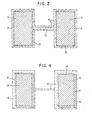
- FIG. 4 illustrates a slight misregistration or misalignment of the optically exposed pattern part of FIG. 2 with respect to the electron beam exposed pattern part.
- the optical exposure pattern and the electron beam exposure pattern overlap.
- the pattern to be formed in a resist layer is the T pattern 30 shown in FIG. 5.1.
- the edges of the desired T pattern are first biased or moved inward to compensate for the edge creep (or movement of edges) which occurs when a nominally exposed pattern is developed.
- the amount of this bias depends upon the composition and thickness of the radiation sensitive material to be exposed, as well as the type and dose of the pattern exposure at the edges thereof, the type and length of development, etc. In general the amount of bias needed is determined by exposing and developing a test pattern and then measuring the resulting amount of edge creep.
- FIG. 5.2 An edge biased T pattern is shown in FIG. 5.2.
- This biased pattern is also subdivided into two elemental shapes (a rectangle 32 and a square 34) as'is ordinarily done for a pattern to be electron beam written. Partitioning of electron beam patterns is done generally in order to facilitate data compaction and to simplify implementation of a pattern generator for controlling electron beam writing. Partitionment is not actually required by the method of this invention.
- FIG. 5.3 the edges of each of the elemental shapes are delineated by electron beam exposure bands to form an electron beam exposure pattern 36.
- edge band parts 38, 40 lie within the-T figure and do not actually delineate any outside edges of the complete pattern. This results in unnecessary electron beam exposure of some regions which could have been optically exposed, but it has no detrimental effect upon the resulting exposure pattern. If the electron beam writing system can just as well and just as efficiently expose only the outside edges of a complete unpartitioned pattern, then such an electron beam pattern is preferable assuming no other disadvantages are generated as a result.
- FIG. 5.4 illustrates an alternative electron beam exposure pattern 36 corresponding to an unpartitioned exposure pattern.
- optical exposure pattern 42 Superposed upon the electron beam exposure pattern 36 of F I G. 5.3 is an optical exposure pattern 42.
- the illustrated optical exposure pattern also covers or overlaps edge band parts 38, 40, which do not correspond with outside edges of the complete pattern. It is alternatively possible in FIG. 5.3 to exclude edge band parts 38, 40 from the optical exposure pattern, if desired.
- Optical exposure pattern 42 is also shown . in FIG. 5.4.
- the composite exposure pattern in FIG. 5.4 will now be used to form a resist pattern.
- the electron beam exposure pattern 36 is applied to a radiation sensitive resist layer 44 on an object 46 using a steered electron beam 48.
- Suitable resists for this purpose are, for example, Shipley AZ1350J resist, Shipley AZ2400 resist, or a polymethylmethacrylate (PMMA) resist.
- the optical exposure pattern 42 is applied to the radiation sensitive resist layer 44 by imaging a mask 50 with an optical flood beam 52.
- the mask 50 may be prepared using standard lithographic techniques such as electron beam lithography.
- a flood source 52 is used which emits light (preferably ultraviolet) in a range where the resist is sensitive.
- Alignment of the mask 50 with respect to the exposure pattern 36 is done using standard alignment techniques.
- Preferably both the electron beam exposure pattern 36 and the mask 50 are each. registered with respect to alignment marks (not shown) carried by the object 46.
- Imaging of the mask onto the resist layer 44 may be done using contact or proximity or projection printing lithography techniques.
- the exposed resist layer 44 has been developed. If'the resist is positive acting, the exposed regions will dissolve away, as shown, leaving a T-shaped opening through the resist layer. If the resist is negative acting, the unexposed regions of the resist layer will dissolve away instead.
Landscapes
- Engineering & Computer Science (AREA)
- Chemical & Material Sciences (AREA)
- Physics & Mathematics (AREA)
- Nanotechnology (AREA)
- General Physics & Mathematics (AREA)
- Crystallography & Structural Chemistry (AREA)
- Mathematical Physics (AREA)
- Theoretical Computer Science (AREA)
- Condensed Matter Physics & Semiconductors (AREA)
- Manufacturing & Machinery (AREA)
- Analytical Chemistry (AREA)
- Electron Beam Exposure (AREA)
- Exposure And Positioning Against Photoresist Photosensitive Materials (AREA)
- Exposure Of Semiconductors, Excluding Electron Or Ion Beam Exposure (AREA)
Abstract
Description
- This invention relates to methods of forming exposure patterns. Such patterns are formed during lightographic processes.
- Electron beams can be formed with a very small diameter and have been used to write very high resolution patterns for microcircuit fabrication. Small diameter electron beams have been used not only as a direct writing lithography tool during fabrication of high density microcircuits but also indirectly to form high resolution masks for use in fabricating microcircuits.
- Unfortunately, serial exposure of a high resolution electron beam pattern is very time consuming. The high-cost of electron beam exposure systems and the relatively low thruput when high density lithographic exposure patterns of practical size are being formed (at best only a dozen pattern exposures per hour) has limited the direct manufacturing use of electron beam lithography, Particularly as a direct writing microcircuit fabrication tool. There is a need for much higher thruput (i.e. more pattern exposures per hour per electron beam exposure system).
- In an article by T. Barker and S. Bernacki entitled "Dual-Polarity, Single-Resist Mixed (E-Beam/Photo Lithography," IEEE Electron Device Letters, Vol. EDL-2, No. 11, pp. 281-283 (Nov. 1981), a method is described in which small geometries or shapes in a pattern are exposed with an electron beam system and large geometries or shapes in the same pattern are exposed with light.
- A problem which has impeded more extensive use of high resolution electron beam lithography is "proximity effect." When an electron beam penetrates a material, such as an electron beam sensitive resist, the high energy primary electrons in the beam collide with molecules in the material and become laterally deflected or scattered in a random process. Secondary electrons are also released by the collisions and travel not only in the forward direction but also laterally and in the backward direction. Back scattering of secondary electrons is particularly great at material interfaces such as the boundary between an electron beam sensitive resist and a supporting substrate. The lateral spreading of the primary and secondary electrons causes nearby lateral regions to be exposed to scattered electrons. When two regions to be exposed are positioned close together, each receives not only the direct electron beam exposure during irradiation of that region, but also an extra dose of electron beam exposure due to the lateral scattering or spreading of electrons during exposure of the adjacent region. As a result, closely adjacent regions become more heavily exposed from the same incident dose than do isolated regions. Accordingly, when an electron beam sensitive resist is exposed to an entire pattern at a constant incident electron beam dose, electron beam exposed regions which are adjacent to other electron beam exposed regions develop differently than do isolated electron beam exposed regions. This has become known as the proximity effect.
- A prior art method for avoiding proximity effects is to compensate for the expected added exposure contributed by electrons scattered from adjacent regions by correspondingly reducing the incident exposure dose of the region. Elaborate computer programs have been developed which calculate the dose needed at each elemental region of a complex pattern so as to get a substantially uniform total exposure everywhere in the pattern. Isolated regions get a greater incident exposure than regions adjacent to other regions.
- While this technique is highly effective, it is also rather expensive due to the high cost of developing such programs and the extra expense in making the extensive computer calculations required, storing the dose data, and developing, fabricating and maintaining electron beam equipment having a computer controlled variable dose capability.
- Another problem with the prior art technique of varying the exposure dose in order to compensate for proximity effect is that this technique cannot be used at all when the exposure process inherently produces a uniform incident exposure dose everywhere in the exposure pattern. This occurs, for example, if a mask is illuminated with an electron flood beam to form an electron beam exposure pattern or if a patterned layer directly emits a pattern of electrons. Such electron beam shadow masks and patterned electron emitters are not in practical use at this time but future development of such techniques is possible.
- In the specification of co-pending European patent application No. 83109313.3, a technique is described for modifying an electron beam exposure pattern so as to make the exposure pattern less sensitive to proximity effects, without computing the exposure contribution from adjacent shapes due to lateral scattering and without requiring that the applied electron beam exposure dose be varied. Unfortunately, this technique does not significantly change the thruput of the electron beam exposure system.
- It is an object of this invention to reduce the amount of electron beam exposure system time required in making a high resolution pattern exposure.
- Another object is to improve electron beam exposure system thruput while maintaining electron beam resolution everywhere in the pattern and while maintaining a developed edge profile everwhere characteristic of an electron beam pattern exposure.
- It is also an object of this invention to simultaneously reduce or eliminate electron beam proximity effects without requiring that the applied exposure dose be varied.
- Still another object is to provide a pattern exposure method having improved electron beam exposure system thruput and reduced electron beam proximity effects without requiring computation of the exposure contribution from adjacent shapes due to lateral scattering effects.
- A complete lithographic exposure pattern is formed in accordance with this invention by forming part of the complete pattern with electron beam radiation and forming the remaining part with light radiation. The electron beam exposure pattern part delineates all of the edges of the desired complete pattern while the optical exposure pattern part fills in any remaining regions, together forming the desired complete exposure pattern. Since all edges are delineated by electron beam radiation, any radiation sensitive layer exposed to the complete pattern will develop edges characteristic of an electron beam pattern exposure.
- Electron beam exposure system thruput is improved because the whole pattern in not exposed by electron beam. Preferably, the exposure width of the electron beam edge delineation is on the order of the minimum linewidth of the pattern, so that proximity effects will be automatically reduced or eliminated without requiring computation of the exposure contribution from adjacent shapes in the pattern due to lateral scattering effects and without requiring any variation in the applied electron beam exposure dose. Use of a wider exposure width for electron beam delineation of pattern edges has the advantage that alignment tolerance of the optical exposure pattern part with respect to the electron beam exposure pattern part is increased.
- More specifically the invention provides a method of forming an exposure pattern comprising the steps of; forming an electron beam exposure pattern corresponding with edge regions of a desired complete exposure pattern; forming an optical exposure pattern corresponding with non-edge regions of said desired complete exposure pattern; and superposing said electron beam exposure pattern and said optical exposure pattern to form said desired complete exposure pattern.
- The invention also provides a method of forming a lithographic resist exposure pattern, comprising the steps of: delineating the edges of a desired resist pattern by exposing a radiation sensitive resist layer to a pattern of electron beam radiation corresponding with the edges of said desired resist pattern; filling in the non-edge regions of said desired resist pattern by exposing said radiation sensitive resist layer to a pattern of light radiation corresponding with the non-edge regions of said desired resist pattern; and developing said exposed resist layer to form said desired resist pattern.
- The invention will now be further described with reference to the accompanying drawings, in which:-
- FIG. 1 illustrates a simple overall exposure pattern formed in accordance with this invention by superposing an electron beam exposure pattern and optical exposure pattern.
- FIG. 2 shows the same overall exposure pattern formed by superposing modified electron beam and optical exposure patterns which improve pattern misalignment tolerance.
- FIG. 3. illustrates an overall exposure pattern where electron scattering is relied upon to provide some of the pattern exposure.
- FIG. 4 shows the electron beam and optical exposure patterns of FIG. 2 in misalignment but producing the same overall exposure pattern.
- FIGS. 5.1-5-4 step-by-step illustrate the formation of constituent electron beam and optical exposure pattern parts for another simple overall exposure pattern.
- FIGS. 6.1-6.3 illustrate formation of a resist pattern using the exposure process of this invention.
- FIG. 1 illustrates a simple overall exposure pattern consisting of two large
rectangular areas edge pattern part 16 is stippled while thenon-edge pattern part 18 is hatched. - Preferably the edge delineation with electron beam should be as narrow as practical in order to reduce undesirable proximity effects. Undesirable proximity effects arise primarily from the excessive number of scattered electrons which are generated when an electron beam exposes a relatively large area. By avoiding any large area electron beam exposures, the present invention automatically avoids proximity effects in large part.
- In FIG. 1, it has been assumed that the narrow bar 14 has a width equal to the minimum linewidth of the overall exposure pattern. Accordingly, the narrow bar 14 has been entirely exposed using electron beam radiation. Preferably, the other edges are delineated with a band of electron beam radiation also about equal to the minimum linewidth of the overall exposure pattern, as shown in FIG. 1. It is possible, however, for the width of the electron beam edge delineation to be either wider or narrower than the exposure pattern minimum linewidth.
- If the electron beam exposure system can form an electron beam exposed band of a width less than the exposure pattern minimum linewidth and sufficiently accurate alignment of the optical and electron beam patterns can be done, an edge delineation of less width than the minimum linewidth might further reduce undesirable proximity effects. A wider electron beam edge delineation is shown in FIG. 2. As will become more apparent, a wider edge delineation with electron beam is useful, for example, for reducing the alignment accuracy required when superposing or overlaying the electron beam exposure pattern and the optical exposure pattern in accordance with this invention. Unfortunately optical exposure patterns are difficult to form at a resolution of better than about one-half micron or so. X-ray lithography might in the future extend this limit to some extent. The present resolution limits for optical lithography, however, suggests a practical minimum width for the electron beam edge bands of about one- half micron.
- In FIG. 2 the
optical exposure part 18 overlaps the electronbeam exposure part 16. Just the reverse is shown in FIG. 3 where there is a nominallyunexposed band 20 between the optically exposedpart 18 and the electron beam exposedpart 16. A nominally unexposed band can be tolerated because electrons will be scattered into the nominally unexposed band from the adjacent electron beam exposed band. Also, as a practical matter, any line having a nominal exposure width will always develop into a somewhat wider line. This edge creep during development of an exposed pattern can be relied upon to remove a nominally unexposed band of suitably narrow width. A nominallyunexposed band 22 of suitably narrow width also may be present between two electron beam exposed edge delineations, as illustrated in FIG. 3. This nominallyunexposed band 22 also will disappear during development, if it is sufficiently narrow. - FIG. 4 illustrates a slight misregistration or misalignment of the optically exposed pattern part of FIG. 2 with respect to the electron beam exposed pattern part. In FIG. 2, the optical exposure pattern and the electron beam exposure pattern overlap. In FIG. 4, due to the misalignment there are
regions 24 where the optical exposure pattern and the electron beam exposure pattern do not overlap at all andother regions 26 where they overlap much more than FIG. 2. Fortunately, media which are sensitive both to electron beam and light radiation generally develop similarly (except perhaps at edges) even when exposed to both. - As previously described, suitably narrow unexposed bands will disappear during development while increased overlap of electron beam and optical exposure parts has no significant effect so long as the outside edge is still defined by the electron beam radiation. Consequently, a radiation sensitive layer exposed to the misregistered superposed pattern illustrated in FIG. 4 will develop into substantially the same final pattern as would a radiation sensitive layer exposed to the correctly registered superposed pattern shown in FIG. 2. This tolerance to some misalignment between the optical exposure pattern and the electron beam exposure pattern generally improves with the width of the electron beam edge delineation and the overlap between optical and electron beam patterns.
- Use of the process to form a lithographic resist pattern will now be described in detail. It will be assumed that the pattern to be formed in a resist layer is the
T pattern 30 shown in FIG. 5.1. The edges of the desired T pattern are first biased or moved inward to compensate for the edge creep (or movement of edges) which occurs when a nominally exposed pattern is developed. The amount of this bias depends upon the composition and thickness of the radiation sensitive material to be exposed, as well as the type and dose of the pattern exposure at the edges thereof, the type and length of development, etc. In general the amount of bias needed is determined by exposing and developing a test pattern and then measuring the resulting amount of edge creep. - An edge biased T pattern is shown in FIG. 5.2. This biased pattern is also subdivided into two elemental shapes (a
rectangle 32 and a square 34) as'is ordinarily done for a pattern to be electron beam written. Partitioning of electron beam patterns is done generally in order to facilitate data compaction and to simplify implementation of a pattern generator for controlling electron beam writing. Partitionment is not actually required by the method of this invention. - In FIG. 5.3, the edges of each of the elemental shapes are delineated by electron beam exposure bands to form an electron
beam exposure pattern 36. It should be noted that as a result of fully edge delineating shapes which are not separate from each other,edge band parts beam exposure pattern 36 corresponding to an unpartitioned exposure pattern. - Superposed upon the electron
beam exposure pattern 36 of FIG. 5.3 is anoptical exposure pattern 42. The illustrated optical exposure pattern also covers or overlapsedge band parts edge band parts Optical exposure pattern 42 is also shown . in FIG. 5.4. - The composite exposure pattern in FIG. 5.4 will now be used to form a resist pattern. In FIG. 6.1, the electron
beam exposure pattern 36 is applied to a radiation sensitive resistlayer 44 on anobject 46 using a steeredelectron beam 48. Suitable resists for this purpose are, for example, Shipley AZ1350J resist, Shipley AZ2400 resist, or a polymethylmethacrylate (PMMA) resist. - In FIG. 6.2 the
optical exposure pattern 42 is applied to the radiation sensitive resistlayer 44 by imaging amask 50 with anoptical flood beam 52. Themask 50 may be prepared using standard lithographic techniques such as electron beam lithography. Aflood source 52 is used which emits light (preferably ultraviolet) in a range where the resist is sensitive. Alignment of themask 50 with respect to theexposure pattern 36 is done using standard alignment techniques. Preferably both the electronbeam exposure pattern 36 and themask 50 are each. registered with respect to alignment marks (not shown) carried by theobject 46. Imaging of the mask onto the resistlayer 44 may be done using contact or proximity or projection printing lithography techniques. - In FIG. 6.3 the exposed resist
layer 44 has been developed. If'the resist is positive acting, the exposed regions will dissolve away, as shown, leaving a T-shaped opening through the resist layer. If the resist is negative acting, the unexposed regions of the resist layer will dissolve away instead. - It should be apparent to one of ordinary skill that certain changes and modifications can be made to the present invention. For example, while formation of a complete exposure pattern has been described by first exposing with an electron beam exposure pattern and then by exposing with an optical exposure pattern, the order of the exposures could be reversed and the two exposures could in theory be done simultaneously. Also, while the electron beam exposure pattern was illustrated as being generated by direct writing with a steered electron beam, it is possible in theory to use an electron beam mask or patterned electron emitter instead. The optical exposure pattern also could be generated in theory using a steered optical beam. These and further modifications may be made without departing from the scope of the present invention, which is defined by the following claims.
Claims (12)
Applications Claiming Priority (2)
| Application Number | Priority Date | Filing Date | Title |
|---|---|---|---|
| US06/451,682 US4717644A (en) | 1982-12-20 | 1982-12-20 | Hybrid electron beam and optical lithography method |
| US451682 | 1989-12-18 |
Publications (2)
| Publication Number | Publication Date |
|---|---|
| EP0111707A2 true EP0111707A2 (en) | 1984-06-27 |
| EP0111707A3 EP0111707A3 (en) | 1986-09-10 |
Family
ID=23793273
Family Applications (1)
| Application Number | Title | Priority Date | Filing Date |
|---|---|---|---|
| EP83110956A Withdrawn EP0111707A3 (en) | 1982-12-20 | 1983-11-03 | Methods of forming exposure patterns |
Country Status (3)
| Country | Link |
|---|---|
| US (1) | US4717644A (en) |
| EP (1) | EP0111707A3 (en) |
| JP (1) | JPS59117214A (en) |
Cited By (1)
| Publication number | Priority date | Publication date | Assignee | Title |
|---|---|---|---|---|
| EP1887614A4 (en) * | 2005-06-03 | 2008-12-24 | Advantest Corp | Patterning method |
Families Citing this family (22)
| Publication number | Priority date | Publication date | Assignee | Title |
|---|---|---|---|---|
| JPS6247129A (en) * | 1985-08-26 | 1987-02-28 | Fujitsu Ltd | Manufacture of semiconductor device |
| JP2617923B2 (en) * | 1986-09-16 | 1997-06-11 | 松下電子工業株式会社 | Pattern formation method |
| US4812962A (en) * | 1987-04-09 | 1989-03-14 | Harris Corp. | Area feature sorting mechanism for neighborhood-based proximity correction in lithography processing of integrated circuit patterns |
| US4816361A (en) * | 1987-11-27 | 1989-03-28 | The United States Of America As Represented By The Secretary Of The Army | Patterning optical and X-ray masks for integrated circuit fabrication |
| US4797334A (en) * | 1987-12-14 | 1989-01-10 | The United States Of America As Represented By The Secretary Of The Army | Patterning optical and X-ray masks for integrated circuit fabrication |
| JP2680074B2 (en) * | 1988-10-24 | 1997-11-19 | 富士通株式会社 | Method of manufacturing semiconductor device using charged particle beam exposure |
| JPH02210814A (en) * | 1989-02-10 | 1990-08-22 | Fujitsu Ltd | Manufacture of semiconductor device |
| US5182718A (en) * | 1989-04-04 | 1993-01-26 | Matsushita Electric Industrial Co., Ltd. | Method and apparatus for writing a pattern on a semiconductor sample based on a resist pattern corrected for proximity effects resulting from direct exposure of the sample by a charged-particle beam or light |
| JP2834797B2 (en) * | 1989-10-25 | 1998-12-14 | 株式会社リコー | Thin film forming equipment |
| DE68923880T2 (en) * | 1989-12-18 | 1996-04-18 | Ibm | Process for the production of complementary patterns for the exposure of semiconductor bodies with self-supporting masks. |
| US5327338A (en) * | 1990-01-31 | 1994-07-05 | Etec Systems, Inc. | Scanning laser lithography system alignment apparatus |
| US5379233A (en) * | 1991-07-19 | 1995-01-03 | Lsi Logic Corporation | Method and structure for improving patterning design for processing |
| US6109775A (en) * | 1991-07-19 | 2000-08-29 | Lsi Logic Corporation | Method for adjusting the density of lines and contact openings across a substrate region for improving the chemical-mechanical polishing of a thin-film later disposed thereon |
| US5159201A (en) * | 1991-07-26 | 1992-10-27 | International Business Machines Corporation | Shape decompositon system and method |
| US5251140A (en) * | 1991-07-26 | 1993-10-05 | International Business Machines Corporation | E-beam control data compaction system and method |
| US5663893A (en) * | 1995-05-03 | 1997-09-02 | Microunity Systems Engineering, Inc. | Method for generating proximity correction features for a lithographic mask pattern |
| US6529621B1 (en) * | 1998-12-17 | 2003-03-04 | Kla-Tencor | Mechanisms for making and inspecting reticles |
| US6516085B1 (en) | 1999-05-03 | 2003-02-04 | Kla-Tencor | Apparatus and methods for collecting global data during a reticle inspection |
| US6778695B1 (en) * | 1999-12-23 | 2004-08-17 | Franklin M. Schellenberg | Design-based reticle defect prioritization |
| US6966047B1 (en) | 2002-04-09 | 2005-11-15 | Kla-Tencor Technologies Corporation | Capturing designer intent in reticle inspection |
| JP2004136432A (en) * | 2002-09-24 | 2004-05-13 | Nihon Micro Coating Co Ltd | Polishing cloth and its manufacturing method |
| JP5499761B2 (en) * | 2010-02-23 | 2014-05-21 | 富士通セミコンダクター株式会社 | Exposure method and semiconductor device manufacturing method |
Family Cites Families (8)
| Publication number | Priority date | Publication date | Assignee | Title |
|---|---|---|---|---|
| US4165395A (en) * | 1977-06-30 | 1979-08-21 | International Business Machines Corporation | Process for forming a high aspect ratio structure by successive exposures with electron beam and actinic radiation |
| JPS5541785A (en) * | 1978-09-20 | 1980-03-24 | Fujitsu Ltd | Pattern exposing method |
| JPS5556629A (en) * | 1978-10-21 | 1980-04-25 | Chiyou Lsi Gijutsu Kenkyu Kumiai | Pattern forming method |
| US4264711A (en) * | 1979-12-10 | 1981-04-28 | Burroughs Corporation | Method of compensating for proximity effects in electron-beam lithography |
| JPS56125830A (en) * | 1980-03-07 | 1981-10-02 | Hitachi Ltd | Uniform exposure patterning method in electron beam patterning device |
| JPS573318A (en) * | 1980-08-20 | 1982-01-08 | Hitachi Maxell | Switch unit for miniature electric equipment |
| JPS5848919A (en) * | 1981-09-18 | 1983-03-23 | Nec Corp | Preparation of semiconductor device |
| EP0104235A4 (en) * | 1982-03-29 | 1984-09-14 | Motorola Inc | Electron beam-optical hybrid lithographic resist process. |
-
1982
- 1982-12-20 US US06/451,682 patent/US4717644A/en not_active Expired - Fee Related
-
1983
- 1983-11-03 EP EP83110956A patent/EP0111707A3/en not_active Withdrawn
- 1983-11-29 JP JP58223383A patent/JPS59117214A/en active Pending
Cited By (1)
| Publication number | Priority date | Publication date | Assignee | Title |
|---|---|---|---|---|
| EP1887614A4 (en) * | 2005-06-03 | 2008-12-24 | Advantest Corp | Patterning method |
Also Published As
| Publication number | Publication date |
|---|---|
| US4717644A (en) | 1988-01-05 |
| EP0111707A3 (en) | 1986-09-10 |
| JPS59117214A (en) | 1984-07-06 |
Similar Documents
| Publication | Publication Date | Title |
|---|---|---|
| US4717644A (en) | Hybrid electron beam and optical lithography method | |
| US6096458A (en) | Methods for manufacturing photolithography masks utilizing interfering beams of radiation | |
| DE112004001942T5 (en) | Combined pattern with trenches | |
| US7229723B2 (en) | Method for forming an opening in a light-absorbing layer on a mask | |
| US4610948A (en) | Electron beam peripheral patterning of integrated circuits | |
| KR100412017B1 (en) | Exposure method and x-ray mask structure for use with the same | |
| KR20000047560A (en) | Exposure method | |
| US6555275B2 (en) | Technique of exposing a resist using electron beams having different accelerating voltages, and method of manufacturing a photomask using the technique | |
| US4122335A (en) | Method and apparatus for mask to wafer gap control in X-ray lithography | |
| KR20000047561A (en) | Exposure method | |
| US6168904B1 (en) | Integrated circuit fabrication | |
| US4604345A (en) | Exposure method | |
| Sakakibara et al. | Variable-shaped electron-beam direct writing technology for 1-µm VLSI fabrication | |
| JPH0787174B2 (en) | Pattern formation method | |
| Tsudaka et al. | Practical optical proximity effect correction adopting process latitude consideration | |
| Harriott | A new role for e-beam: Electron projection | |
| KR100253581B1 (en) | Lithography process method | |
| JPS60229001A (en) | Manufacture of integrated diffraction grating | |
| JPS5948538B2 (en) | Electron beam exposure method | |
| JPS58102939A (en) | Masks for mask aligners and mask aligners | |
| JPS59141230A (en) | Formation of pattern | |
| KR940011203B1 (en) | Process for producing pattern | |
| KR100209370B1 (en) | Mask for superimposition measurement mark and manufacturing method of superimposition mark using the same | |
| JPS5721819A (en) | Forming method for pattern | |
| JP2716296B2 (en) | Pattern formation method |
Legal Events
| Date | Code | Title | Description |
|---|---|---|---|
| PUAI | Public reference made under article 153(3) epc to a published international application that has entered the european phase |
Free format text: ORIGINAL CODE: 0009012 |
|
| AK | Designated contracting states |
Designated state(s): DE FR GB |
|
| 17P | Request for examination filed |
Effective date: 19841029 |
|
| PUAL | Search report despatched |
Free format text: ORIGINAL CODE: 0009013 |
|
| AK | Designated contracting states |
Kind code of ref document: A3 Designated state(s): DE FR GB |
|
| 17Q | First examination report despatched |
Effective date: 19880808 |
|
| STAA | Information on the status of an ep patent application or granted ep patent |
Free format text: STATUS: THE APPLICATION HAS BEEN WITHDRAWN |
|
| 18W | Application withdrawn |
Withdrawal date: 19890717 |
|
| R18W | Application withdrawn (corrected) |
Effective date: 19890717 |
|
| RIN1 | Information on inventor provided before grant (corrected) |
Inventor name: JONES, FLETCHER Inventor name: ROELKER, HENRY RUDOLF |