EP0109106A1 - Schaltung zur Signalpegelumsetzung zwischen gesättigter und ungesättigter Logik - Google Patents
Schaltung zur Signalpegelumsetzung zwischen gesättigter und ungesättigter Logik Download PDFInfo
- Publication number
- EP0109106A1 EP0109106A1 EP83201475A EP83201475A EP0109106A1 EP 0109106 A1 EP0109106 A1 EP 0109106A1 EP 83201475 A EP83201475 A EP 83201475A EP 83201475 A EP83201475 A EP 83201475A EP 0109106 A1 EP0109106 A1 EP 0109106A1
- Authority
- EP
- European Patent Office
- Prior art keywords
- transistor
- logic
- circuit
- terminal
- potential
- Prior art date
- Legal status (The legal status is an assumption and is not a legal conclusion. Google has not performed a legal analysis and makes no representation as to the accuracy of the status listed.)
- Granted
Links
Images


Classifications
-
- H—ELECTRICITY
- H03—ELECTRONIC CIRCUITRY
- H03K—PULSE TECHNIQUE
- H03K19/00—Logic circuits, i.e. having at least two inputs acting on one output; Inverting circuits
- H03K19/0175—Coupling arrangements; Interface arrangements
- H03K19/018—Coupling arrangements; Interface arrangements using bipolar transistors only
- H03K19/01806—Interface arrangements
Definitions
- the present invention relates to a signal level converter circuit between, on the one hand, a first logic of saturated type with two output signal levels, supplied by a first continuous supply, one of the terminals of which constitutes the common reference for potential and, on the other hand, a second logic of the unsaturated type at two other signal levels, supplied by a second continuous supply, one of the terminals of which is connected to the common reference of potential and the other terminal is at a voltage of polarity opposite to that of the other terminal of the first continuous supply, a transit terminal receiving in particular the output signals of the first logic to be converted into signals, on an output terminal of the converter, at the levels suitable for the input of the second logic.
- TTL type logic is very widespread in all cases where low consumption is required and the switching speed is not an absolute imperative, as in the case of peripheral organs for example.
- a logic of the ECL / CML type with current switching, proves faster by the absence of saturation and the reduction of the logical excursion. It is therefore advantageously used within central bodies that have to process digital information at very high speed.
- a converter circuit as defined in the preamble is known in particular from the patent of the United States of America at 3,959,666.
- the voltage at the switching threshold does not have the desirable variability as a function of the temperature, that is to say a variability corresponding to two direct voltage drops of semiconductor junctions as is the case. case for TTL type logic. It follows that the noise immunity of such a circuit cannot meet the standard requirements over the entire range of temperatures usually specified.
- the known circuit calls for the use of a Schottky diode in parallel on the base-collector junction of a transistor so as to avoid saturation of this transistor.
- the integration of this type of diode if it is easy when the converter circuit is produced according to a TTL technology, may become impossible on the other hand when one wishes to produce it according to certain CML technologies.
- the Schottky diode or replacing it with an anti-saturation transistor.
- the saturation of the transistor leads to a loss of speed which is not acceptable.
- the diode is replaced by a transistor to which two additional resistors must be added so that the circuit then requires a number relatively high components to achieve the desired switching speed.
- the invention proposes in particular to remedy the drawbacks of the circuits of the prior art.
- a first object of the invention aims to preserve a good adaptation between the signal levels of the two logic elements in a wide range of operating temperatures.
- Another object of the invention is to provide a converter circuit of simple structure and the elements of which can be integrated with a complex function of the second logic and defined according to the same technological rules.
- point of the circuit with potential defined with respect to that of the common reference is meant the common reference in itself or else a point whose potential deviates from that of the common reference of a stable value such as that of a direct semiconductor junction voltage drop, for example.
- Charge element for the constant current source means any element such as a resistor, a diode, a transistor providing a suitable voltage drop when the current supplied by the constant current source is passed through.
- semiconductor junction designates not only a diode but also, and preferably, a transistor connected as a diode, that is to say of which the base and the collector are connected and form one of the output electrodes, the transmitter forming the other electrode.
- the converter circuit according to the invention offers the advantage of being made up of a limited number of elements which can be easily integrated within said second logic.
- the circuit does not include a terminal of the first continuous supply such as + V DC in the case where the first logic is constituted by TTL.
- the excursions between levels of the input and output signals of the converter circuit can be kept compatible over a very wide temperature range.
- the base of the emitter follower transistor is connected to the transit terminal via a series connection comprising a current limiting resistor and at least one additional direct semiconductor junction.
- the collector of the emitter follower transistor is connected to one of the nodes of said serial connection.
- the collector of the emitter follower transistor can be connected at will, either directly to the terminal transit, either at the node connecting the limiting resistor to the additional semiconductor junction, or even directly at the base of the same transistor.
- the order of the elements of the series connection can still be reversed and the choice for connecting the collector remains.
- the value of the limiting resistance must be chosen differently depending on whether the collector current of the emitter follower transistor crosses this resistance or not.
- the transit terminal which supplies the control signals for the base of the emitter follower transistor also supplies the collector current of this transistor when necessary.
- the first embodiment of the invention comprises a particular variant according to which an additional limiting resistor is inserted in said series connection between the node to which the collector of the emitter follower transistor is connected and the base of said transistor.
- This variant offers the advantage of reducing the current supplied by the transit terminal.
- the converter circuit is characterized in that said first point of the circuit is connected to a first electrode of an annex semiconductor junction, junction whose second electrode is connected to the reference common, an auxiliary current source being moreover connected between the first electrode of the auxiliary semiconductor junction and said other terminal of the second power supply, which subjects the auxiliary semiconductor junction to a sense current direct, and that said serial connection comprises two additional semiconductor junctions.
- This mode of implementation therefore consists in shifting the value of a direct voltage drop of a semiconductor junction the control of the base of the emitter follower transistor with respect to the first mode of implementation. It follows that one can then advantageously connect the collector of the emitter follower transistor to the common reference. The collector current is then supplied by the common reference and no longer by the transit terminal, which reduces the current consumption on this terminal.
- a particularly advantageous variant for the second embodiment of the invention, but which is also applicable to the first mode, consists in that an additional source of current, in particular an additional base resistance is connected between the base of the transistor follower transmitter and said other terminal of the second power supply.
- This additional current source chosen to deliver a weak current compared to that delivered by said constant current source makes it possible to reduce the influence of the gain of the follower emitter transistor on the operation of the converter circuit to the point that this influence becomes negligible.
- said second point of the circuit with defined potential is connected to said first point.
- the charging element consists of a transistor of the same polarity as the emitter follower transistor, hereinafter called charge transistor, the emitter of which constitutes said first connection, of which the base constitutes said second connection which is subjected to the potential of one of the internal levels of the second logic and the collector of which is connected to the common reference.
- Such a variant advantageously applies to the case of a converter circuit in which the transit terminal can also receive, for a transfer to the first logic, signals coming from an output circuit of the second logic comprising a first pair of transistors with coupled emitters mounted in "OR" gate for the control of a first transistor of a second pair of transistors with coupled emitters, remarkable in that one of the bases of the first pair of transistors constitutes a first input for selection of conversion mode, the other base of the same pair receiving the signals of the second logic, in that in the link to the reference common of the collector of the first transistor of the second pair is inserted a semiconductor junction which constitutes said annex semiconductor junction, while a current source supplying the second pair constitutes said annex current source, in that the collector of the second transistor of the second pair is connected to the common reference via a direct semiconductor junction and, on the other hand, is connected to the transit terminal, and in that the base of the t
- the charge transistor constitutes a second mode selection input, controlled additionally with respect to the first selection input.
- the converter circuit 10 is represented by a general diagram surrounded by a dashed frame.
- a circuit of a first logic 11, of saturated type, TTL for example, is supplied from a first continuous supply 14 whose negative terminal 15 constitutes the common reference of potential M.
- the potential commonly called V CC is delivered by the positive terminal 16 of the power supply 14.
- a circuit of a second logic 12, of the unsaturated type such as the ECL or CML logic, is delimited by a dashed frame marked with 12, a frame which is shown attached to the converter circuit 10 because the circuits 10 and 12 are preferably integrated simultaneously in the same semiconductor body.
- the circuit of the second logic 12 is supplied by a second continuous supply 20, the positive terminal of which is at the common reference of potential M.
- V EE ' The potential, commonly called V EE ' is delivered by the negative terminal 21 of the supply 20.
- the output signals of the circuit of the first logic 11 are present on the output terminal 17 which is connected to the V CC via a resistor R C , external to the circuit 11, resistor serving as a load at the collector of a transistor Tll at the output of the circuit 11.
- the output terminal 17 is connected to a transit terminal 22 belonging to the converter circuit 10.
- the converter circuit 10 comprises a follower emitter transistor Tl the base of which is, on the one hand, connected to a first point Pl of the circuit 10 at potential defined with respect to that of the common reference M, via a first semiconductor junction JI mounted in the direct direction and, on the other hand, connected to the transit terminal 22 via a connection series 23 comprising in particular a resistor R1, current limiter, and at least one additional semiconductor junction J2, mounted in the direct direction.
- the semiconductor junctions J1 and J2 have been shown as diodes but it is clear that, for the specialist, advantageously used as semiconductor junctions J1 and J2 are transistors connected by diode. This remark also extends to other semiconductor junctions which will be discussed later in the presentation.
- the converter circuit 10 also comprises a constant current source SI of structure usual in ECL / CML technique in particular, connected between V EE and the emitter of the follower emitter transistor T1.
- the constant current source SI delivers a current of value I.
- the converter circuit 10 finally comprises a charging element Z, a first connection 24 of which is connected to the emitter of the emitter follower transistor Tl, and a second connection 25 is connected to a second point P2 of the circuit 10 at potential defined relative to that of the common reference M.
- the output terminal 27 of the converter circuit 10 is common to the first connection 24 of the charging element Z.
- the output terminal 27 carries the signals for the input of the circuit of the second logic 12. These signals have their low level determined, from the potential of the second point P2, by the voltage drop in the load element Z traversed by the current I, the emitter follower transistor Tl being blocked in response to a low level of the transit terminal 22, then that the high level of the signals carried by the output terminal 27 is determined by the potential of the emitter of the follower emitting transistor Tl when the latter is conductive, in response to a high level of the transit terminal 22.
- the high level of the output terminal 27 corresponds very substantially to the potential of the first point Pl since the semiconductor junction J1 practically balances the voltage V BE of the emitter follower transistor Tl.
- terminal 28 of the collector of transistor Tl can be connected to one or other suitable node of circuit 10 depending on the case, node chosen so that in conduction mode, transistor Tl can debit an emitter current of value practically equal to I, while avoiding saturation.
- circuit of the second logic 12 we have been content, for the record, to represent a differential input stage 30 for which the signal carried by the terminal 27 is applied to one of the input bases , the other base being brought to a reference potential V R.
- the structure of the circuit of the second logic 12 indeed falls within the field of known art, in particular for the type of ECL / CML logic, and is not part of the invention.
- FIG. 2 shows the electrical diagram of the converter circuit of FIG. 1, the common elements of which are given the same references, and indicates a first embodiment of the invention.
- the diagram in FIG. 2 differs from the corresponding part of FIG. 1 by the following connections: the points P1 and P2 are connected together to the common reference M and the collector terminal 28 of the transistor Tl is connected to the serial connection 23 on the conductor which connects the resistor R1 and the semiconductor junction J2.
- the load element Z is constituted by a resistance of value R.
- V T can be evaluated approximately by means of the expression (1): V T ⁇ R1.I / 2 + V J2 + V BE (T1) - RI / 2 in which the value of the base current has been neglected before that emitter and collector currents of transistor Tl, values taken as equal to each other.
- V J2 designates the direct voltage drop in the semiconductor junction J2, while V BE (T1), that of the transistor Tl in the base emitter junction.
- a TTL logic is characterized by a tilting level whose value, of the order of 1.3 volts, varies according to the temperature as two drops in voltage of junctions.
- the converter circuit of the example described the compatibility of the tilting levels desirable, depending on the temperature, between the two logics since the output tilt level remains stable as is suitable for CML logic.
- the potential of the transit terminal rises above the level of tilting to the high state of the first logic.
- the emitting current of transistor Tl increases until it reaches the value of I.
- the current in R is then canceled and terminal 27 reaches the high state, at 0 volts.
- the semiconductor junction J1 enters into conduction and the high state of the terminal 27 is maintained at 0 volts.
- the input current of the circuit 10 is limited by the limiting resistor R1.
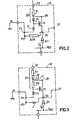
- FIG. 3 illustrates a converter circuit similar to that of Figure 2, but with some variants.
- the elements common to Figures 1 and 2 are assigned the same reference signs.
- the circuit of FIG. 3 is distinguished in that the limiting resistor R1 being connected directly to the transit terminal, the collector of the emitter follower transistor Tl connected to a first electrode 31 of the semiconductor junction J2, an additional limiting resistor R2 is inserted in the series connection 23 between the first electrode 31 of the junction J2 and the base of the transistor T1.
- the second electrode 32 of the junction J2 is connected to the limiting resistor R1.
- Another variant with respect to FIG. 2 resides in the fact that the charging element for the current source SI is a semiconductor junction J, connected in the direct direction relative to this current source.
- the circuit of FIG. 3 operates in a manner quite similar to that of the circuit of FIG. 2.
- the transistor T1 When the potential of the transit terminal 22 is in the low state, the transistor T1 is blocked.
- the current I crosses the junction J creating on terminal 27 a low state whose potential is equal to: (0 - V J ) volt, V J designating the direct voltage drop in the junction J crossed by the current I.
- the value (V J ) also represents the level excursion at the input of the second logic, ie 0.7 to 0.8 volts depending on the value of the current I and the characteristics of the junction J which have been chosen.
- the introduction of the additional limiting resistor R2 therefore offers the advantage of being able to significantly reduce the input current of the circuit 10 in the state high, while the value of the resistance R1 remains the predominant parameter which determines the adjustment of the tilting level of the first logic. It is clear that the introduction of the additional limiting resistor R2, considered as a first variant with respect to the diagram in FIG. 2, is a variant which is not linked to the second variant which consisted in using, as load element, a junction J instead of a resistor R.
- the third variant introduced in FIG. 3 resides in the choice of the point where the collector of the transistor T1 has been connected to the series connection 23 which is different from that shown in FIG. 2.
- FIG. 4 shows the example of a second embodiment of the converter circuit according to the invention, as defined by the general diagram of FIG. 1.
- the elements common to those of FIG. 1 are given the same signs landmarks.
- the load element for the current source SI is a resistor R.
- the operation of the converter circuit of this example is now briefly explained: when the transit terminal 22 is in the low state , the transistor Tl is blocked. Indeed, the offset of the potential of the base of Tl, due to the voltage drop in the junction J4, is compensated by the additional junction J3.
- the current source S3 has the effect of reinforcing the blocking of T1.
- the output terminal 27 is in the low state whose potential is equal to (- VJ4 - RI), ie a level excursion of the second logic defined by the term RI, negatively shifted from a direct voltage drop at the junction J4.
- V T then reached by the transit terminal 22 can be evaluated approximately by expression (3): expression which can still be summarized as: where V J designates a direct junction voltage drop.
- FIG. 5 shows another example of the converter circuit according to the invention, the structure of which is close to that of the example in FIG. 4, but in an application to a bidirectional conversion of signals between the two logics.
- the elements of FIG. 5 which are common to those of FIG. 4 are assigned identical references insofar as they fulfill a similar function.
- the logic CML within which the converter circuit 100 has been physically integrated, is a logic with complex function, for example a network of prediffused gates or a memory. Only the portions relating to the invention have been shown, namely: an input CML circuit 120 for the input of signals from the TTL logic after conversion of the levels by the converter 100, and a CML circuit of output 200 for the output of signals from CML logic and intended for TTL logic. The transit of these signals is carried out by the single transit terminal 22.
- the output CML circuit 200 comprises a first pair of transistors T201, T202 with coupled emitters, mounted in an "OR" gate for the control of a transistor T203 forming, with a transistor T204, a second pair.
- the collectors of the transistors T201 and T202 are connected to ground M (common reference of the two logic).
- the common conductor of the transmitters is connected to the V EE via a current source S21 and, on the other hand, connected to the base of the transistor T203.
- the base of transistor T204 is brought to a reference potential level V R2 of the logic CML, known as name of "second level" because of its value imposed by the situation of the second pair of transistors relative to the first pair.
- the collector of transistor T204 is connected to ground M via a direct semiconductor junction J5 and, on the other hand, connected to transit terminal 22.
- the collector of transistor T203 is connected to point P1 of converter circuit 100, which is connected to ground M via the semiconductor junction J4 which constitutes the additional semiconductor junction described in connection with FIG. 4.
- the conductor common to the emitters of the second pair of transistors T203, T204 is connected to V EE via a current source S2 shown within the converter circuit 100, because it fulfills the function of the secondary current source S2 of the example in FIG. 4.
- At the base of the transistor T202 are applied signals coming from the CML logic and which are intended to be transferred as TTL input signals on the bus 220.
- the base of transistor T201 constitutes a first conversion mode selection input, which is subjected to a selection signal A.
- the converter circuit 100 is analogous to the circuit 10 of FIG. 4 with a few differences.
- the load element of the current source S1 is constituted here by a transistor T z instead of a resistor.
- the charge transistor T Z has the same polarity as the follower emitting transistor Tl. Its emitter constitutes what was previously called the first connection of the charging element, its base constitutes the second connection connected to point P2 which is subject to the potential of one of the CML internal levels. More precisely, at point P2, and therefore at the base of transistor T Z , a signal A is applied which is complementary to the mode selection signal A whose levels are defined with respect to V R1 , "first level" reference. The base of T Z therefore constitutes a second mode selection input, controlled in addition to the first selection input.
- the additional current source is constituted here by a simple additional basic resistance R3, of high value, replacing the additional current source S3 described in FIG. 4.
- This resistance R3 is connected between the base of the transistor Tl and V EE .
- the output terminal 27 of the converter circuit 100 carries signals which, coming from the TTL logic and after conversion, are applied to the input CML circuit 120 of which only the first differential stage 30 has been shown. This stage is, by elsewhere, referenced to V R2 , second level reference.
- the selection signal A When the selection signal A is in the high state, the transistor T201 conducts, the transistor T203 also conducts, and this independently of the signal applied to the base of the transistor T202.
- the junction J4 is supplied with current from the current source S2 via the transistor T203.
- the transistor T204 is blocked, its collector constitutes a high impedance for the transit terminal 22 which is then free to receive by the bus 220 the signals coming from the TTL logic.
- a selection signal A in the high state is therefore a signal selecting the mode: TTL output towards CML input.
- the signal A applied to P2 is then in the low state, of the order of - 0.4 volts. If, under these circumstances, the transit terminal 22 is in the low state, the transistor T1 does not conduct.
- the current I of the current source S1 crosses the charge transistor T z creating on terminal 27 a low state whose potential is equal to (0.4 - V BE (TZ) ) volt-, or approximately - 1.2 volt.
- V BE (TZ) designates the emitter-base voltage drop of the load transistor T Z.
- V T corresponds to the tilting level of the TTL logic, ie twice the direct voltage drop of a junction.
- V R2 the second level reference potential corresponds to the sum of a direct junction voltage drop and a half-excursion of logic level CML.
- I 0.5 mA
- I3 0.1 mA, which allows the value of the resistance R3 to be determined.
- a logic half-excursion CML being, in general, close to 0.2 volts, we arrive at R1 ⁇ 1.90 KSL for a gain of 50, of the transistor T1 and R1 ⁇ 1.95 K ⁇ for a gain ⁇ of 100. It is observed that it is easy to choose values for which the operation of the circuit is very little affected by variations in gain of the transistors, from one batch to another, during the manufacture of circuits according to the invention, under an integrated form.
- Terminal 27 reaches a high state fixed by the potential of P1 since the voltage drops V J1 and V BE (T1) substantially offset each other.
- the high state of terminal 27 therefore corresponds to a potential of the order of - 0.8 volts imposed by the voltage offset relative to ground M due to the junction J4 supplied directly.
- the mode selection signal A is in the low state. Its complementary AT, applied to P2 is high, close to 0 volts.
- the charge transistor T Z is conductive and carries the terminal 27 in the high, forced state, of - 0.8 volts, a state which the transistor Tl cannot modify in response to a signal carried by the transit terminal 22.
- the converter circuit 100 can no longer transmit signals from the TTL logic to the CML circuit 120, whose differential stage 30 is blocked in the high state on its input.
- the transit terminal 22 is brought to a low state, of approximately ⁇ 0.8 volts, determined by the voltage drop relative to the mass M, in the junction J5.
- the transistor T203 does not flow; the junction J4 is not supplied, but the transit terminal 22 being in the low state, the transistor T1 remains blocked.
- the transistor T204 When now, it is the transistor T203 which conducts, the transistor T204 is blocked.
- the transit terminal 22 is free to go back to the high state under the effect of the resistance R C connected to the V CC .
- the current I2 of the current source S2 is supplied, via the transistor T203, in part by the Jl junction and for the rest by the J4 junction.
- the transistor Tl operates under the conditions described above, that is to say that supposing that it conducts, it would impose on terminal 27 the same high state of ⁇ 0.8 volts as that already fixed.
- a selection signal A in the low state, is therefore a signal selecting the mode: CML output towards TTL input.
Landscapes
- Engineering & Computer Science (AREA)
- Computer Hardware Design (AREA)
- Physics & Mathematics (AREA)
- Computing Systems (AREA)
- General Engineering & Computer Science (AREA)
- Mathematical Physics (AREA)
- Logic Circuits (AREA)
Applications Claiming Priority (2)
| Application Number | Priority Date | Filing Date | Title |
|---|---|---|---|
| FR8217397 | 1982-10-18 | ||
| FR8217397A FR2534752A1 (fr) | 1982-10-18 | 1982-10-18 | Circuit convertisseur de niveaux de signaux entre une logique de type saturee et une logique de type non saturee |
Publications (2)
| Publication Number | Publication Date |
|---|---|
| EP0109106A1 true EP0109106A1 (de) | 1984-05-23 |
| EP0109106B1 EP0109106B1 (de) | 1987-01-07 |
Family
ID=9278347
Family Applications (1)
| Application Number | Title | Priority Date | Filing Date |
|---|---|---|---|
| EP83201475A Expired EP0109106B1 (de) | 1982-10-18 | 1983-10-14 | Schaltung zur Signalpegelumsetzung zwischen gesättigter und ungesättigter Logik |
Country Status (5)
| Country | Link |
|---|---|
| US (1) | US4612460A (de) |
| EP (1) | EP0109106B1 (de) |
| JP (1) | JPS59103427A (de) |
| DE (1) | DE3369041D1 (de) |
| FR (1) | FR2534752A1 (de) |
Cited By (1)
| Publication number | Priority date | Publication date | Assignee | Title |
|---|---|---|---|---|
| EP0366294A2 (de) * | 1988-10-06 | 1990-05-02 | Nec Corporation | TTL-ECL-Pegelumsetzungsschaltung |
Families Citing this family (5)
| Publication number | Priority date | Publication date | Assignee | Title |
|---|---|---|---|---|
| JPH0763139B2 (ja) * | 1985-10-31 | 1995-07-05 | 日本電気株式会社 | レベル変換回路 |
| US5059826A (en) * | 1989-11-30 | 1991-10-22 | Motorola Inc. | Voltage threshold generator for use in diode load emitter coupled logic circuits |
| US5008570A (en) * | 1990-03-30 | 1991-04-16 | The United States Of America As Represented By The Secretary Of The Air Force | Schmitt-triggered TTL to CML input buffer apparatus |
| DE4201947C2 (de) * | 1992-01-24 | 1993-10-28 | Texas Instruments Deutschland | Integrierte Transistorschaltung mit Reststromkompensation |
| US5440248A (en) * | 1994-01-31 | 1995-08-08 | Texas Instruments Incorporated | Power-saver differential input buffer |
Citations (2)
| Publication number | Priority date | Publication date | Assignee | Title |
|---|---|---|---|---|
| US3660676A (en) * | 1970-01-07 | 1972-05-02 | Siemens Ag | Circuit arrangement for converting signal voltages |
| EP0052565A1 (de) * | 1980-11-17 | 1982-05-26 | FAIRCHILD CAMERA & INSTRUMENT CORPORATION | Gegen Temperatur- und Herstellungsschwankungen kompensierter TTL-ECL-Verknüpfungspuffer |
Family Cites Families (8)
| Publication number | Priority date | Publication date | Assignee | Title |
|---|---|---|---|---|
| GB1245347A (en) * | 1968-07-01 | 1971-09-08 | Nippon Telegraph & Telephone | Improved high speed logic circuit device |
| US3716722A (en) * | 1970-04-29 | 1973-02-13 | Cogar Corp | Temperature compensation for logic circuits |
| US3959666A (en) * | 1974-07-01 | 1976-05-25 | Honeywell Information Systems, Inc. | Logic level translator |
| US3986045A (en) * | 1975-04-23 | 1976-10-12 | Advanced Micro Devices, Inc. | High speed logic level converter |
| JPS56117427A (en) * | 1980-02-20 | 1981-09-14 | Fujitsu Ltd | Level converting circuit |
| US4456838A (en) * | 1981-02-25 | 1984-06-26 | Tokyo Shibaura Denki Kabushiki Kaisha | Level shifting circuit |
| JPS57162838A (en) * | 1981-03-31 | 1982-10-06 | Fujitsu Ltd | Emitter coupling type logical circuit |
| US4518876A (en) * | 1983-03-30 | 1985-05-21 | Advanced Micro Devices, Inc. | TTL-ECL Input translation with AND/NAND function |
-
1982
- 1982-10-18 FR FR8217397A patent/FR2534752A1/fr active Granted
-
1983
- 1983-10-14 DE DE8383201475T patent/DE3369041D1/de not_active Expired
- 1983-10-14 US US06/541,946 patent/US4612460A/en not_active Expired - Fee Related
- 1983-10-14 EP EP83201475A patent/EP0109106B1/de not_active Expired
- 1983-10-18 JP JP58195148A patent/JPS59103427A/ja active Granted
Patent Citations (2)
| Publication number | Priority date | Publication date | Assignee | Title |
|---|---|---|---|---|
| US3660676A (en) * | 1970-01-07 | 1972-05-02 | Siemens Ag | Circuit arrangement for converting signal voltages |
| EP0052565A1 (de) * | 1980-11-17 | 1982-05-26 | FAIRCHILD CAMERA & INSTRUMENT CORPORATION | Gegen Temperatur- und Herstellungsschwankungen kompensierter TTL-ECL-Verknüpfungspuffer |
Non-Patent Citations (1)
| Title |
|---|
| IBM TECHNICAL DISCLOSURE BULLETIN, vol. 12, no. 2, juillet 1969, page 296, New York, US * |
Cited By (2)
| Publication number | Priority date | Publication date | Assignee | Title |
|---|---|---|---|---|
| EP0366294A2 (de) * | 1988-10-06 | 1990-05-02 | Nec Corporation | TTL-ECL-Pegelumsetzungsschaltung |
| EP0366294A3 (de) * | 1988-10-06 | 1990-12-05 | Nec Corporation | TTL-ECL-Pegelumsetzungsschaltung |
Also Published As
| Publication number | Publication date |
|---|---|
| US4612460A (en) | 1986-09-16 |
| DE3369041D1 (en) | 1987-02-12 |
| FR2534752A1 (fr) | 1984-04-20 |
| JPS59103427A (ja) | 1984-06-14 |
| EP0109106B1 (de) | 1987-01-07 |
| JPH0432571B2 (de) | 1992-05-29 |
| FR2534752B1 (de) | 1984-11-23 |
Similar Documents
| Publication | Publication Date | Title |
|---|---|---|
| EP0029767B1 (de) | Steuerungsverfahren einer Darlingtonschaltung und Darlingtonschaltung mit geringen Verlusten | |
| EP0432058B1 (de) | Dynamische Isolierschaltung für integrierte Schaltungen | |
| EP0201136B1 (de) | Digitales Multiplexermodul mit N-Eingängen und solche Module enthaltender Multiplexer mit N-Quadrat-Eingängen | |
| EP0194177B1 (de) | Teilnehmerschnittstellenschaltung mit Überwachungsbetrieb bei verringerter Speisung | |
| FR2529729A1 (fr) | Reseau de bascules | |
| EP0700151A1 (de) | Leistungsfolgeverstärkerstufe | |
| FR2470485A1 (fr) | Amplificateurs equilibres de classe ab | |
| EP0109106B1 (de) | Schaltung zur Signalpegelumsetzung zwischen gesättigter und ungesättigter Logik | |
| EP0080395A1 (de) | Bistabile Kippschaltung mit energieunabhängiger Haltbarkeit und dynamischer Rücksetzung | |
| EP0237094A1 (de) | Vordiffundierte Gatterfeld-Halbleitervorrichtung für speziell hergestellte Schaltungen | |
| FR2738424A1 (fr) | Interrupteur analogique basse tension | |
| EP0601922B1 (de) | Mehrbitwort organisierter EEPROM Speicher | |
| EP0281465B1 (de) | Speicherleseverstärker | |
| EP0860948B1 (de) | Pufferverstärker für Bussteuerung | |
| FR2477802A1 (fr) | Circuit d'amplification | |
| EP0899921B1 (de) | Symmetrischer Leitungstreiber | |
| EP1111788B1 (de) | Rekonfigurierbare Schaltmatrix insbesondere für Weltraumanwendungen | |
| EP0553020B1 (de) | TTL-CMOS-Ausgangsstufe für integrierte Schaltungen | |
| EP0700162B1 (de) | Logische Schaltung mit Differenzstufen | |
| EP0203645A1 (de) | Integrierte Digital/Analog-Wandlerschaltung mit Gerät zur Glitchreduzierung | |
| EP0301979B1 (de) | Brückenschaltung zur Basisansteuerung mit selbst im Lawinen-Modus gesteuerter Sperrung | |
| EP0187572B1 (de) | Begrenzerschaltung für logische Spannungsabweichungen und eine solche Begrenzerschaltung enthaltende logische Schaltung | |
| FR2619972A1 (fr) | Etage amplificateur differentiel et configurations de circuits utilisant un tel etage | |
| EP0763282B1 (de) | Schnittstelle zum umsetzen logischer ecl-pegel in cmos-pegel | |
| FR2589296A1 (fr) | Circuit de commande en parallele d'un grand nombre de cellules logiques de type stl |
Legal Events
| Date | Code | Title | Description |
|---|---|---|---|
| PUAI | Public reference made under article 153(3) epc to a published international application that has entered the european phase |
Free format text: ORIGINAL CODE: 0009012 |
|
| AK | Designated contracting states |
Designated state(s): DE FR GB NL |
|
| 17P | Request for examination filed |
Effective date: 19840719 |
|
| RAP1 | Party data changed (applicant data changed or rights of an application transferred) |
Owner name: N.V. PHILIPS' GLOEILAMPENFABRIEKEN Owner name: RTC-COMPELEC |
|
| GRAA | (expected) grant |
Free format text: ORIGINAL CODE: 0009210 |
|
| AK | Designated contracting states |
Kind code of ref document: B1 Designated state(s): DE FR GB NL |
|
| PG25 | Lapsed in a contracting state [announced via postgrant information from national office to epo] |
Ref country code: NL Effective date: 19870107 |
|
| REF | Corresponds to: |
Ref document number: 3369041 Country of ref document: DE Date of ref document: 19870212 |
|
| NLV1 | Nl: lapsed or annulled due to failure to fulfill the requirements of art. 29p and 29m of the patents act | ||
| PLBE | No opposition filed within time limit |
Free format text: ORIGINAL CODE: 0009261 |
|
| STAA | Information on the status of an ep patent application or granted ep patent |
Free format text: STATUS: NO OPPOSITION FILED WITHIN TIME LIMIT |
|
| 26N | No opposition filed | ||
| REG | Reference to a national code |
Ref country code: FR Ref legal event code: CA |
|
| REG | Reference to a national code |
Ref country code: FR Ref legal event code: CD |
|
| PGFP | Annual fee paid to national office [announced via postgrant information from national office to epo] |
Ref country code: FR Payment date: 19931020 Year of fee payment: 11 |
|
| PGFP | Annual fee paid to national office [announced via postgrant information from national office to epo] |
Ref country code: DE Payment date: 19931223 Year of fee payment: 11 |
|
| PGFP | Annual fee paid to national office [announced via postgrant information from national office to epo] |
Ref country code: GB Payment date: 19940930 Year of fee payment: 12 |
|
| PG25 | Lapsed in a contracting state [announced via postgrant information from national office to epo] |
Ref country code: FR Effective date: 19950630 |
|
| PG25 | Lapsed in a contracting state [announced via postgrant information from national office to epo] |
Ref country code: DE Effective date: 19950701 |
|
| REG | Reference to a national code |
Ref country code: FR Ref legal event code: ST |
|
| PG25 | Lapsed in a contracting state [announced via postgrant information from national office to epo] |
Ref country code: GB Effective date: 19951014 |
|
| GBPC | Gb: european patent ceased through non-payment of renewal fee |
Effective date: 19951014 |