EP0107844B1 - Einrichtung zur Feststellung von Fehlern in metallischen Rohren mit Hilfe von Wirbelströmen - Google Patents
Einrichtung zur Feststellung von Fehlern in metallischen Rohren mit Hilfe von Wirbelströmen Download PDFInfo
- Publication number
- EP0107844B1 EP0107844B1 EP83110480A EP83110480A EP0107844B1 EP 0107844 B1 EP0107844 B1 EP 0107844B1 EP 83110480 A EP83110480 A EP 83110480A EP 83110480 A EP83110480 A EP 83110480A EP 0107844 B1 EP0107844 B1 EP 0107844B1
- Authority
- EP
- European Patent Office
- Prior art keywords
- defect
- phase
- signal
- eddy current
- detecting system
- Prior art date
- Legal status (The legal status is an assumption and is not a legal conclusion. Google has not performed a legal analysis and makes no representation as to the accuracy of the status listed.)
- Expired
Links
Images


Classifications
-
- G—PHYSICS
- G01—MEASURING; TESTING
- G01N—INVESTIGATING OR ANALYSING MATERIALS BY DETERMINING THEIR CHEMICAL OR PHYSICAL PROPERTIES
- G01N27/00—Investigating or analysing materials by the use of electric, electrochemical, or magnetic means
- G01N27/72—Investigating or analysing materials by the use of electric, electrochemical, or magnetic means by investigating magnetic variables
- G01N27/82—Investigating or analysing materials by the use of electric, electrochemical, or magnetic means by investigating magnetic variables for investigating the presence of flaws
- G01N27/90—Investigating or analysing materials by the use of electric, electrochemical, or magnetic means by investigating magnetic variables for investigating the presence of flaws using eddy currents
- G01N27/9046—Investigating or analysing materials by the use of electric, electrochemical, or magnetic means by investigating magnetic variables for investigating the presence of flaws using eddy currents by analysing electrical signals
Definitions
- the present invention relates to an eddy current defect-detecting system, and more particularly to an eddy current defect-detecting system for metal tubes which is capable of determining defects on inner and outer surfaces and detecting the depth of a defect based on the phase of a flaw or defect of a defect signal which phase varies with the conditions of the defect formed on a metal tube, that is, the location and depth of the defect.
- Prior eddy current defect-detecting systems have a test coil with a high-frequency current flowing therethrough.
- the test coil is inserted into a metal tube for electrically measuring a variation in the amplitude of an eddy current generated by a flaw (hereinafter referred to as a "defect") present on the metal tube.
- a defect an eddy current generated by a flaw
- the variation in the eddy current is quite small, it is amplified by a detector (hereinafter referred to as a "bridge") and an amplifier and then converted into a voltage.
- the signal includes a defect-indicative signal component and noise due to wobbling of the coil caused when the latter is inserted into the metal tube being tested.
- This test method is known as an amplitude method which indicates the shape and depth of a defect with one signal for evaluation of the defect.
- the conventional eddy current defect-detecting systems fail to tell a defect with a large thickness reduction in a narrow area from a defect accompanying a small thickness reduction in a wide area, and hence are liable to judge a metal tube suffering only from a small thickness reduction and still usable as requiring replacement.
- US-A-3 302 105 relates to a device for nondestructively testing a sample.
- a probe having first and second inductive impedances is used and a relative motion is provided between the probe and the sample.
- Said impedances are fixedly spatially mounted with respect to each other.
- a difference signal varying in phase and amplitude is generated and means are provided for detecting said difference signal.
- Recording means are used to generate a display which serves to identify and determine the location of irregularities in said material as they are traversed by said probe.
- Patent abstract of Japan Vol. 6 Number 18, 2nd February, 1982, page (P-100) discloses a discriminating method for signals in eddy current flow detection.
- Two phase detectors respectively, detect specific signals.
- An arithmetic part is used to synthesize the detection output components of two orthogonal axes to operate and calculate peculiar signal locus patterns so as to determine an angle alpha.
- This angle alpha is compared with a set value, and depending upon whether it is below or above the determined value, the flaw signal and noise signal are discriminated easily and accurately.
- Another object of the present invention is to provide an eddy current defect-detecting system for metal tubes which is capable of accurately and quickly measuring a defect on an outer or inner surface of a metal tube and the depth of the defect.
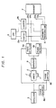
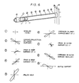
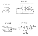
- an eddy current defect-detecting system basically comprises a detector 2 including a pair of test coils 1, 1', an oscillator 3, a pair of phase detectors 4a, 4b, a picture display 5, an arithmetic processing unit 6, a recorder 7, a phase adjuster 8a, a phase shifter 8b, an amplifier 9, and choppers 13a, 13b. More specifically, as shown in Fig. 6, the test coils 1, l' are wound around a probe 11 in axially juxtaposed relation and movable axially through a metal tube 10 being tested for detecting as an impedance variation a variation in an eddy current generated due to a defect or dent present in the metal tube 10.
- the detector 2 comprises a bridge including the test coils 1, 1' as illustrated in Fig. 10.
- the oscillator 3 is connected to the bridge 2 for exciting the bridge 2 at a high frequency such that an eddy current flows within the wall of the metal tube.
- the phase adjuster 8a is connected to the oscillator 3 and the bridge 2 and is responsive to an oscillated output from the oscillator 3 for adjusting its phase to produce a first control signal.
- the phase shifter 8b is connected to an output terminal of the phase adjuster 8a for producing a second control signal by shifting the phase of the first control signal by 90°.
- the amplifier 9 is connected to an output terminal of the bridge 2 and serves as a tuning amplifier for amplifying a signal of a required frequency only.
- the phase detectors 4a, 4b are coupled to an output terminal of the amplifier 9 for producing a first defect signal or X-axis signal by effecting first phase detection on an output signal from the bridge 2 with the first control signal and a second defect signal or Y-axis signal by effecting second phase detection on the output signal from the bridge 2 with the second control signal which is 90° out of phase with the first control signal.
- the arithmetic processing unit 6 which is in the form of a central processing unit is coupled to output terminals of the phase detectors 4a, 4b for electrically reading amplitudes of the first and second defect signals from the phase detectors 4a, 4b to find phase angles thereof indicative of whether a detected defect is on an inner surface or an outer surface of the metal tube and of the depth of the defect.
- the recorder 7 which is of the multi-channel type is connected to the phase detectors 4a, 4b and the arithmetic processing unit 6 for recording a defect on an inner surface (hereinafter referred to as an "inner defect") and its depth and a defect on an outer surface (hereinafter referred to as an "outer defect”) and its depth.
- the choppers 13a, 13b are connected to the output terminals, respectively, of the phase detectors 4a, 4b for converting the issued defect signals into AC signals of a fixed frequency having amplitudes proportional to the magnitudes of the defect signals.
- the picture display 5 comprises a cathode-ray tube 5 coupled to output terminals of the choppers 13a, 13b and having X- and Y-axis input terminals receptive of output signals from the choppers 13a, 13b for displaying defect patterns as Lissajous figures on the screen.
- An AC signal is supplied from the oscillator 3 (Fig. 1) to the bridge 2, and impedances Z (Fig. 10) in the bridge 2 are varied to balance the latter.
- the test coils 1, 1' which are wound around the probes 11 movable axially through the metal tube being tested as shown in Figs. 1 and 6 coact with an eddy current generated in the metal tube 10, and vary their impedance dependent on the condition of the metal tube 10.
- the impedance variation of the test coils 1, 1' is converted by the bridge 2 into an electric signal which is issued through its output terminal.
- the test frequency is determined by the bridge 3 and selected taking into account a skin effect (penetration depth), defects and other factors.
- a test frequency should be selected which is optimum for the test speed, the material of the metal tube, and the relationship between the shape and dimensions of the metal tube and the penetration depth.
- the oscillator 3 is of the variable-frequency type generally comprising a CR oscillator or a crystal oscillator.
- the output signal from the bridge 2 is delivered through the amplifier 9 to the phase detectors 4a, 4b. While various designs are available of the phase detectors 4a, 4b, those employing electronic switching circuits are generally used. As shown in Fig. 2(a), the phase detectors 4a, 4b are energized by the control signals to allow the input signals to appear as output signals during a half period in which the phase of the control signals ranges from 0 to n.
- the phase detectors 4a, 4b are de-energized to disable their output terminals.
- signals which are ⁇ out of phase with the control signals are applied to the input terminals of the phase detectors 4a, 4b, they produce an output waveform as shown in Fig. 2(a).
- the output signals have a waveform symmetrical with respect to the horizontal axis. With this output waveform averaged, no voltage appears on the output terminals of the phase detectors 4a, 4b.
- the DC output voltages from the phase detectors 4a, 4b will now be derived by using mathematical formulas. Assuming that the input signals are ⁇ out of phase with the control signals which give a phase reference, the input signals are expressed by 2V sin ( ⁇ t+ ⁇ ), and the DC voltage E obtained by averaging the outputs from the phase detectors 4a, 4b can be expressed as follows:
- the phase of a signal produced by a defect be Vs
- the phase thereof be ⁇ s
- the voltage of a signal caused by vibrations due to the movement of the coil detector in the metal tube (wobbling of the test coils as they move through the metal tube) be Vn
- the phase thereof be ⁇ n.
- the phase c of the control signals can be selected as desired by the phase adjuster 8a.
- the two input signals have respective phases ( ⁇ s ⁇ c), ( ⁇ n ⁇ c) with respect to the reference phase of the control signals.
- the DC voltage of the output signals is derived from the equation (1) as follows:
- the phase shifter 8b produces the second control signal which is 90° out of phase with the first control signal for the control of the phase detector 4b in order to generate the first and second defect signals separately.
- the tube being tested is moved and the phase adjuster 8a is adjusted to minimize indications on the testing device which would result from vibrations due to movement thereof for determining the phase of the control signals.
- the phase adjuster 8a is used in the eddy current defect detector for selecting the phase of the control signals for the phase detectors 4a, 4b as desired.
- the phases hifter 8b and the phase adjuster 8a generally comprise a CR phase shifting circuit in actual use. This circuit has a phase selection knob for rotating a potentiometer POT.
- Fig. 12 illustrates a circuit arrangement for the phase detectors 4a, 4b by way of example.
- the circuit comprises a phase detector including a series-connected switch in the form of a bidirectional field-effect transistor FET.
- the field effect transistor When a positive pulse is applied as a control signal, the field effect transistor is rendered conductive to allow an input signal to appear as an output signal.
- the field-effect transistor When a negative control signal output is applied, the field-effect transistor is cut off to produce no output signal.
- a capacitor C is connected across output terminals to average the output signal.
- X- and Y-axis signals serving as defect signals are issued from the phase detectors 4a, 4b, respectively. These signals are applied through the choppers 13a, 13b to the cathode-ray tube 5.
- the cathode-ray tube 5 displays output signals from the choppers 13a, 13b in the form of vectors and is used when observing defect signals and other noise phase relationships.
- the images on the cathode-ray tube 5 are displayed as Lissajous figures including straight lines and ellipses.
- each of the choppers 13a, 13b includes a pair of transistors Trl, Tr2 having bases to which a drive signal is applied to turn on and off the junctions between emitters and collectors.
- the choppers 13a, 13b serve as switches intermittently energizable dependent on the drive frequency for generating an AC output.
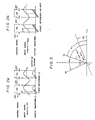
- a signal V having a phase advanced by (p with respect to a signal (X axis) giving a phase reference can be broken into a reference signal component Vx and a component Vy advanced in phase by 90°.
- the phase detectors 4a, 4b produce output DC voltage signals which are expressed from the equation (1) as follows: It is understood from the equations (5) and (6) that the voltages Ex, Ey are proportional respectively to the components Vx, Vy.
- the bright spot thereon which moves in proportion to the input voltage displays the signal voltage V as a vector as shown in Fig. 4(b).
- the phases of the control signals for the two phase detectors 4a, 4b employed to generate the voltages Ex, Ey are varied while keeping the phases 90° out of phase by means of the phase shifter 8b, the phase 0 shown in Fig. 4(a) is also varied. Accordingly, the voltages Ex, Ey also change as is apparent from the equations (6).
- the DC voltages Ex, Ey generated by the phase detectors 4a, 4b are converted by the choppers 13a, 13b into AC signals which are then applied to the horizontal and vertical input terminals of the cathode-ray tube 5.
- the spot on the cathode-ray tube 5 varies in position with time, and displays the input signals a straight line as shown in Fig. 5.
- the angle formed between the displayed straight line and the X axis indicates the phase, and the length of the line indicates the magnitude of the signals.
- the AC signals applied to the horizontal and vertical input terminals are out of phase with each other, the signals are displayed as an ellipse.
- Lissajous figures can be displayed as illustrated in Fig.
- the inclination of a displayed Lissajous figure that is, the phase, permits determination as to whether a defect is an inner defect or an outer defect, and detection of the depth of the defect. More specifically, when the phase is in the range of from 0° to 45°, the defect is an inner defect; when the phase is in the vicinity of 45°, the defect is a through hole; and when the phase ranges from 45° to 180°, the defect is an outer defect.
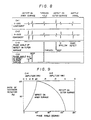
- Fig. 7 shows the steps of processing operation of the arithmetic processing unit 6.
- X- and Y-axis signals from the two phase detectors 4a, 4b are applied to the arithmetic processing unit 6. If the amplitude of the Y-axis signal is 4 mm or more, then the arithmetic processing unit 6 determines the phase of the Y-axis signal. At this time, if a half amplitude of the Y-axis signal is 2 mm or more, then the arithmetic processing unit 6 determines whether the Y-axis signal is positive or negative. No output is issued for channels 3 and 4 of the recorder 7 if the signal has a Y-axis amplitude below the above level.
- the recording level is selected taking noise into account.
- the arithmetic processing unit 6 Only when the Y-axis signal is rising, the phase of the X-axis signal and the amplitudes of the X- and Y-axis signals are read by the arithmetic processing unit 6.
- or A 180 °-tan-'
- the defect is judged as an outer defect, and an output proportional to the phase angle with 180° and 45° as zero and full-scale readings is issued to a channel 3 of the recorder 7.
- the depth of the defect can be measured at this time by a phase angle difference.
- an output is applied to both the channels 3 and 4 of the recorder 7.
- the output mode is selected so that it matches defect images.
- the result of measurement is recorded in the format shown in Fig. 8 on the recorder 7, which comprises a pen recorder.
- any defect can be determined as an inner defect or an outer defect and the ratio of thickness reduction can be measured by reading the phase angle on the cathode-ray tube 5, and also by the used channel (channel 3 or channel 4) of the recorder 7 and the amplitude (mm) of a recorded signal thereon.
Landscapes
- Chemical & Material Sciences (AREA)
- Chemical Kinetics & Catalysis (AREA)
- Electrochemistry (AREA)
- Physics & Mathematics (AREA)
- Health & Medical Sciences (AREA)
- Life Sciences & Earth Sciences (AREA)
- Analytical Chemistry (AREA)
- Biochemistry (AREA)
- General Health & Medical Sciences (AREA)
- General Physics & Mathematics (AREA)
- Immunology (AREA)
- Pathology (AREA)
- Investigating Or Analyzing Materials By The Use Of Magnetic Means (AREA)
Claims (10)
Applications Claiming Priority (2)
| Application Number | Priority Date | Filing Date | Title |
|---|---|---|---|
| JP57185696A JPS5975146A (ja) | 1982-10-21 | 1982-10-21 | 金属管の渦流探傷装置 |
| JP185696/82 | 1982-10-21 |
Publications (3)
| Publication Number | Publication Date |
|---|---|
| EP0107844A2 EP0107844A2 (de) | 1984-05-09 |
| EP0107844A3 EP0107844A3 (en) | 1985-04-10 |
| EP0107844B1 true EP0107844B1 (de) | 1988-08-17 |
Family
ID=16175261
Family Applications (1)
| Application Number | Title | Priority Date | Filing Date |
|---|---|---|---|
| EP83110480A Expired EP0107844B1 (de) | 1982-10-21 | 1983-10-20 | Einrichtung zur Feststellung von Fehlern in metallischen Rohren mit Hilfe von Wirbelströmen |
Country Status (4)
| Country | Link |
|---|---|
| US (1) | US4628260A (de) |
| EP (1) | EP0107844B1 (de) |
| JP (1) | JPS5975146A (de) |
| DE (1) | DE3377740D1 (de) |
Families Citing this family (31)
| Publication number | Priority date | Publication date | Assignee | Title |
|---|---|---|---|---|
| US4814702A (en) * | 1984-05-31 | 1989-03-21 | Westinghouse Electric Corp. | Process for accurately determining the position of the edges of support plates in steam generators |
| FR2570500B1 (fr) * | 1984-09-20 | 1987-03-20 | Siderurgie Fse Inst Rech | Procede et dispositif de detection de defauts typiques sur un produit en defilement, notamment pour la detection de criques sur une brame |
| JPS61147159A (ja) * | 1984-12-20 | 1986-07-04 | Yanagida Sangyo Kk | 探傷装置 |
| US4878180A (en) * | 1985-11-18 | 1989-10-31 | Western Atlas International, Inc. | Method of evaluating the condition of tubular goods |
| US4823082A (en) * | 1986-02-18 | 1989-04-18 | Kabushiki Kaisha Kobe Seiko Sho | Signal processing method for an electromagnetic induction test |
| GB8605280D0 (en) * | 1986-03-04 | 1986-04-09 | Atomic Energy Authority Uk | Magnetic particle inspection techniques |
| JPS63120246A (ja) * | 1986-11-07 | 1988-05-24 | Toda Constr Co Ltd | 地中埋設配管の防食被覆状態の検査方法 |
| DE3720686A1 (de) * | 1987-06-23 | 1989-01-05 | Foerster Inst Dr Friedrich | Verfahren zum untersuchen eines objektes |
| DE3817574A1 (de) * | 1988-05-24 | 1989-11-30 | Fraunhofer Ges Forschung | Wirbelstromsensor |
| JPH0257964A (ja) * | 1988-08-23 | 1990-02-27 | Osaka Gas Co Ltd | 管の渦流探傷による内径と内壁状況の測定方法および装置 |
| GB2224575B (en) * | 1988-11-04 | 1993-07-14 | Technical Software Consultants | Electromagnetic microscope |
| JPH02269957A (ja) * | 1989-04-12 | 1990-11-05 | Mitsui Petrochem Ind Ltd | 探傷用プローブ |
| US5006800A (en) * | 1989-11-06 | 1991-04-09 | General Electric Company | Eddy current imaging apparatus and method using phase difference detection |
| JPH0443978A (ja) * | 1990-06-11 | 1992-02-13 | Seiko Instr Inc | 高感度磁場検出装置 |
| JP2882856B2 (ja) * | 1990-07-04 | 1999-04-12 | 三菱マテリアル株式会社 | 渦流探傷装置 |
| US5424640A (en) * | 1991-01-23 | 1995-06-13 | The United States Of America As Represented By The United States Department Of Energy | Method for removal of random noise in eddy-current testing system |
| EP0518635B1 (de) * | 1991-06-11 | 2003-05-21 | Newt Holdings Limited | Sonde |
| FR2761155B1 (fr) * | 1997-03-20 | 1999-06-04 | Centre Nat Rech Scient | Detecteur de defauts au voisinage d'un alesage |
| GB9718891D0 (en) * | 1997-09-06 | 1997-11-12 | British Gas Plc | Pipeline inspection device |
| US6208181B1 (en) * | 1998-01-14 | 2001-03-27 | Intel Corporation | Self-compensating phase detector |
| US6184226B1 (en) | 1998-08-28 | 2001-02-06 | Scios Inc. | Quinazoline derivatives as inhibitors of P-38 α |
| KR100447482B1 (ko) * | 2001-04-23 | 2004-09-07 | 한국원자력연구소 | 원자력발전소 증기발생기 전열관 균열의 관통 여부 판정및 관통길이 측정방법 |
| US7518359B2 (en) * | 2005-03-09 | 2009-04-14 | General Electric Company | Inspection of non-planar parts using multifrequency eddy current with phase analysis |
| US7557570B2 (en) * | 2005-11-03 | 2009-07-07 | The Clock Spring Company L.P. | System and method for producing color contour maps of surface defects of high pressure pipelines |
| JP4802081B2 (ja) * | 2006-10-31 | 2011-10-26 | 公益財団法人鉄道総合技術研究所 | 厚さ測定装置及び厚さ測定プログラム |
| KR100960895B1 (ko) | 2008-01-28 | 2010-06-04 | 주식회사 유엠아이 | 와전류탐상 데이터 분석방법 |
| JP5269564B2 (ja) * | 2008-11-28 | 2013-08-21 | 非破壊検査株式会社 | 管状体の欠陥評価方法及び管状体の欠陥評価装置 |
| CN108445075A (zh) * | 2018-03-06 | 2018-08-24 | 苏州热工研究院有限公司 | 一种换热管涡流检测管壁损伤的评价方法 |
| CN111351838B (zh) * | 2018-12-20 | 2023-08-18 | 核动力运行研究所 | 一种构造具有特定缺陷的涡流信号的方法 |
| CN111024810B (zh) * | 2019-11-08 | 2022-10-14 | 上海应用技术大学 | 一种能够同时检测不锈钢短管内外壁缺陷的涡流检测装置 |
| CN113777157B (zh) * | 2021-10-09 | 2024-12-20 | 云南电网有限责任公司玉溪供电局 | 基于阻抗谱的电缆铅封缺陷带电检测系统及其检测方法 |
Family Cites Families (7)
| Publication number | Priority date | Publication date | Assignee | Title |
|---|---|---|---|---|
| US3302105A (en) * | 1964-08-26 | 1967-01-31 | Hugo L Libby | Eddy current nondestructive testing device using an oscilloscope to identify and locate irregularities in a test piece |
| US3528003A (en) * | 1967-11-28 | 1970-09-08 | Forster F M O | Sensor for inspecting a test piece for inside and outside flaws utilizing means responsive to the type of flaw for adjusting the threshold of the sensor |
| AU3837372A (en) * | 1971-02-01 | 1973-08-02 | Automation Industries, Inc | Eddy current nondestructive testing system |
| US3848182A (en) * | 1973-08-15 | 1974-11-12 | Magnetic Analysis Corp | Apparatus for limiting phase-angle response range, particularly in eddy current testing apparatus |
| DE2656111C3 (de) * | 1975-12-11 | 1981-02-26 | Magnetic Analysis Corp., Mount Vernon, N.Y. (V.St.A.) | Wirbelstromprüfgerät |
| US4191922A (en) * | 1978-03-14 | 1980-03-04 | Republic Steel Corporation | Electromagnetic flaw detection system and method incorporating improved automatic coil error signal compensation |
| US4424486A (en) * | 1980-10-14 | 1984-01-03 | Zetec, Inc. | Phase rotation circuit for an eddy current tester |
-
1982
- 1982-10-21 JP JP57185696A patent/JPS5975146A/ja active Pending
-
1983
- 1983-10-19 US US06/543,357 patent/US4628260A/en not_active Expired - Fee Related
- 1983-10-20 DE DE8383110480T patent/DE3377740D1/de not_active Expired
- 1983-10-20 EP EP83110480A patent/EP0107844B1/de not_active Expired
Also Published As
| Publication number | Publication date |
|---|---|
| US4628260A (en) | 1986-12-09 |
| EP0107844A2 (de) | 1984-05-09 |
| DE3377740D1 (en) | 1988-09-22 |
| EP0107844A3 (en) | 1985-04-10 |
| JPS5975146A (ja) | 1984-04-27 |
Similar Documents
| Publication | Publication Date | Title |
|---|---|---|
| EP0107844B1 (de) | Einrichtung zur Feststellung von Fehlern in metallischen Rohren mit Hilfe von Wirbelströmen | |
| US5689183A (en) | Electromagnetic-induction type inspection device employing two induction coils connected in opposite phase relation | |
| US3337796A (en) | Eddy current testing device with means for sampling the output signal to provide a signal proportional to the instantaneous value of said output signal at a particular phase | |
| US3197693A (en) | Nondestructive eddy current subsurface testing device providing compensation for variation in probe-to-specimen spacing and surface irregularities | |
| US4683419A (en) | Method and apparatus for detecting faults in a structure by measuring voltage drop between surface points thereof | |
| US3895290A (en) | Defect detection system using an AND gate to distinguish specific flaw parameters | |
| US3546578A (en) | Heterodyned frequency nondestructive testing system utilizing a hall effect device for magnetic field sensing of an eddy current reaction magnetic field | |
| US4792755A (en) | Process and apparatus for the non-destructive examination of ferromagnetic bodies having sections of surface adjoining each other along edges and/or at corners | |
| US4528506A (en) | Ferromagnetic resonance probe liftoff suppression apparatus | |
| US5847562A (en) | Thickness gauging of single-layer conductive materials with two-point non linear calibration algorithm | |
| JPS6314905B2 (de) | ||
| EP0165051A2 (de) | Farbige Schirmbilddarstellung von in Wechselbeziehung stehenden Parametern | |
| US4287474A (en) | Method and apparatus for non-destructive quality testing of spot welds | |
| US3611119A (en) | Method for measuring the ferrite content of a material | |
| US20180217099A1 (en) | Virtual channels for eddy current array probes | |
| JP2003232776A (ja) | 渦流探傷装置および渦流探傷方法 | |
| JPH0545184B2 (de) | ||
| JPH04221757A (ja) | 欠陥検出装置及び方法 | |
| JPH0259947B2 (de) | ||
| JPH102883A (ja) | 渦電流探傷装置 | |
| JP3054778B2 (ja) | Squidによる非破壊検査装置 | |
| US3825820A (en) | Gate circuit for non-destructive testing systems for indicating when test signals lie within predetermined limits | |
| JPH07260743A (ja) | 探傷検査装置 | |
| SU746278A1 (ru) | Способ неразрушающего контрол и устройство дл его реализации | |
| JPH04551B2 (de) |
Legal Events
| Date | Code | Title | Description |
|---|---|---|---|
| PUAI | Public reference made under article 153(3) epc to a published international application that has entered the european phase |
Free format text: ORIGINAL CODE: 0009012 |
|
| AK | Designated contracting states |
Designated state(s): DE FR GB IT NL |
|
| PUAL | Search report despatched |
Free format text: ORIGINAL CODE: 0009013 |
|
| AK | Designated contracting states |
Designated state(s): DE FR GB IT NL |
|
| 17P | Request for examination filed |
Effective date: 19850918 |
|
| 17Q | First examination report despatched |
Effective date: 19861208 |
|
| GRAA | (expected) grant |
Free format text: ORIGINAL CODE: 0009210 |
|
| ITF | It: translation for a ep patent filed | ||
| AK | Designated contracting states |
Kind code of ref document: B1 Designated state(s): DE FR GB IT NL |
|
| REF | Corresponds to: |
Ref document number: 3377740 Country of ref document: DE Date of ref document: 19880922 |
|
| ET | Fr: translation filed | ||
| PLBE | No opposition filed within time limit |
Free format text: ORIGINAL CODE: 0009261 |
|
| STAA | Information on the status of an ep patent application or granted ep patent |
Free format text: STATUS: NO OPPOSITION FILED WITHIN TIME LIMIT |
|
| 26N | No opposition filed | ||
| PGFP | Annual fee paid to national office [announced via postgrant information from national office to epo] |
Ref country code: DE Payment date: 19901029 Year of fee payment: 8 |
|
| ITPR | It: changes in ownership of a european patent |
Owner name: CAMBIO RAGIONE SOCIALE;CXR CO. LTD |
|
| PGFP | Annual fee paid to national office [announced via postgrant information from national office to epo] |
Ref country code: FR Payment date: 19910913 Year of fee payment: 9 |
|
| NLT1 | Nl: modifications of names registered in virtue of documents presented to the patent office pursuant to art. 16 a, paragraph 1 |
Owner name: CXR CO., LTD. TE KURE EN MITSUI PETROCHEMICAL INDU |
|
| REG | Reference to a national code |
Ref country code: FR Ref legal event code: CD |
|
| PGFP | Annual fee paid to national office [announced via postgrant information from national office to epo] |
Ref country code: GB Payment date: 19911015 Year of fee payment: 9 |
|
| ITTA | It: last paid annual fee | ||
| PGFP | Annual fee paid to national office [announced via postgrant information from national office to epo] |
Ref country code: NL Payment date: 19911031 Year of fee payment: 9 |
|
| PG25 | Lapsed in a contracting state [announced via postgrant information from national office to epo] |
Ref country code: DE Effective date: 19920701 |
|
| PG25 | Lapsed in a contracting state [announced via postgrant information from national office to epo] |
Ref country code: GB Effective date: 19921020 |
|
| PG25 | Lapsed in a contracting state [announced via postgrant information from national office to epo] |
Ref country code: NL Effective date: 19930501 |
|
| GBPC | Gb: european patent ceased through non-payment of renewal fee |
Effective date: 19921020 |
|
| NLV4 | Nl: lapsed or anulled due to non-payment of the annual fee | ||
| PG25 | Lapsed in a contracting state [announced via postgrant information from national office to epo] |
Ref country code: FR Effective date: 19930630 |
|
| REG | Reference to a national code |
Ref country code: FR Ref legal event code: ST |